DE275X2-102N06A Datasheet. Specs and Replacement
Type Designator: DE275X2-102N06A 📄📄
Type of Transistor: MOSFET
Type of Control Channel: N-Channel
Absolute Maximum Ratings
Pd ⓘ - Maximum Power Dissipation: 1180 W
|Vds|ⓘ - Maximum Drain-Source Voltage: 1000 V
|Vgs|ⓘ - Maximum Gate-Source Voltage: 20 V
|Id| ⓘ - Maximum Drain Current: 16 A
Tj ⓘ - Maximum Junction Temperature: 175 °C
Electrical Characteristics
Cossⓘ - Output Capacitance: 130 pF
RDSonⓘ - Maximum Drain-Source On-State Resistance: 1.6 Ohm
Package: DE275X2
DE275X2-102N06A substitution
- MOSFET ⓘ Cross-Reference Search
DE275X2-102N06A datasheet
de275x2-102n06a.pdf
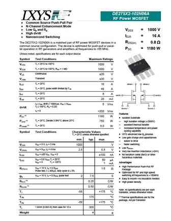
DE275X2-102N06A RF Power MOSFET Common Source Push-Pull Pair N-Channel Enhancement Mode Low Qg and Rg VDSS = 1000 V High dv/dt ID25 = 16 A Nanosecond Switching RDS(on) = The DE275X2-102N06A is a matched pair of RF power MOSFET devices in a 0.8 common source configuration. The device is optimized for push-pull or paral- PDC = 1180 W ... See More ⇒
de275x2-501n16a.pdf
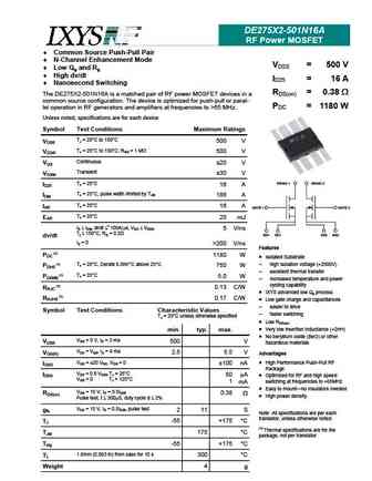
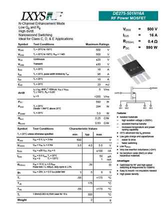
DE275X2-501N16A RF Power MOSFET Common Source Push-Pull Pair N-Channel Enhancement Mode VDSS = 500 V Low Qg and Rg High dv/dt ID25 = 16 A Nanosecond Switching RDS(on) = 0.38 The DE275X2-501N16A is a matched pair of RF power MOSFET devices in a common source configuration. The device is optimized for push-pull or paral- PDC = 1180 W lel operatio... See More ⇒
de275-201n25a.pdf
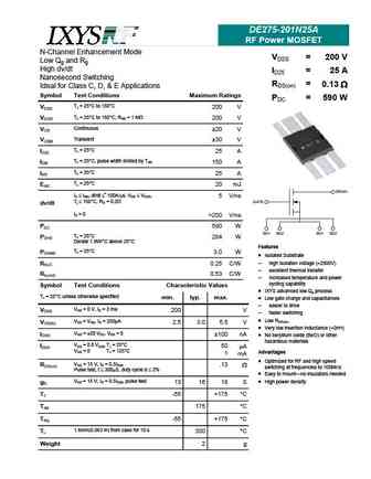
DE275-201N25A RF Power MOSFET N-Channel Enhancement Mode VDSS = 200 V Low Qg and Rg High dv/dt ID25 = 25 A Nanosecond Switching RDS(on) = 0.13 Ideal for Class C, D, & E Applications Symbol Test Conditions Maximum Ratings PDC = 590 W TJ = 25 C to 150 C VDSS 200 V TJ = 25 C to 150 C; RGS = 1 M VDGR 200 V Continuous VGS 20 V Transie... See More ⇒
de275-102n06a.pdf
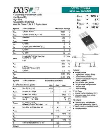
DE275-102N06A RF Power MOSFET N-Channel Enhancement Mode VDSS = 1000 V Low Qg and Rg High dv/dt ID25 = 8 A Nanosecond Switching RDS(on) = 1.5 Ideal for Class C, D, & E Applications PDC = 590 W Symbol Test Conditions Maximum Ratings TJ = 25 C to 150 C VDSS 1000 V TJ = 25 C to 150 C; RGS = 1 M VDGR 1000 V Continuous VGS 20 V Transi... See More ⇒
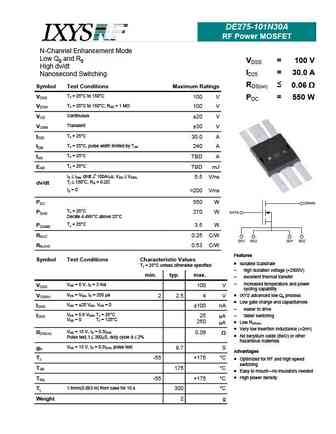
Detailed specifications: DE150-101N09A, DE150-102N02A, DE150-201N09A, DE150-501N04A, DE275-101N30A, DE275-102N06A, DE275-201N25A, DE275-501N16A, 75N75, DE275X2-501N16A, DE375-102N10A, DE375-102N12A, DE375-501N21A, DE475-102N20A, DE475-102N21A, DE475-501N44A, DI9400T
Keywords - DE275X2-102N06A MOSFET specs
DE275X2-102N06A cross reference
DE275X2-102N06A equivalent finder
DE275X2-102N06A pdf lookup
DE275X2-102N06A substitution
DE275X2-102N06A replacement
Need a MOSFET replacement? Our guide shows you how to find a perfect substitute by comparing key parameters and specs
