DMN6040SK3 Specs and Replacement
Type Designator: DMN6040SK3
Type of Transistor: MOSFET
Type of Control Channel: N-Channel
Absolute Maximum Ratings
Pd ⓘ - Maximum Power Dissipation: 42 W
|Vds|ⓘ - Maximum Drain-Source Voltage: 60 V
|Vgs|ⓘ - Maximum Gate-Source Voltage: 20 V
|Id| ⓘ - Maximum Drain Current: 20 A
Tj ⓘ - Maximum Junction Temperature: 150 °C
Electrical Characteristics
tr ⓘ - Rise Time: 8.1 nS
Cossⓘ - Output Capacitance: 57 pF
RDSonⓘ - Maximum Drain-Source On-State Resistance: 0.04 Ohm
Package: TO-252
DMN6040SK3 substitution
- MOSFET ⓘ Cross-Reference Search
DMN6040SK3 datasheet
dmn6040sk3.pdf
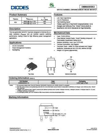
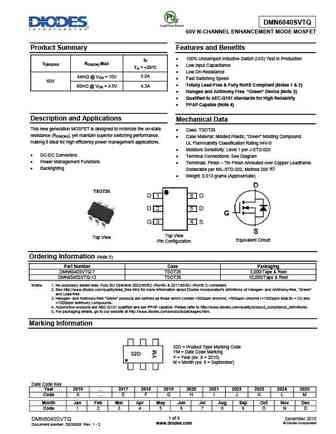
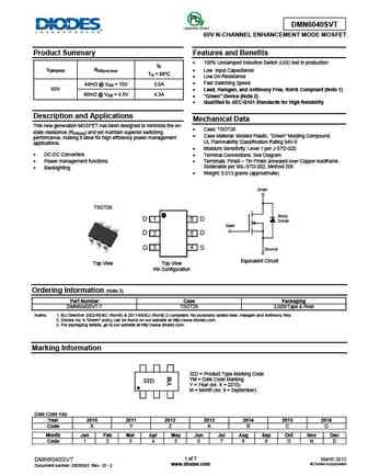
DMN6040SK3 60V N-CHANNEL ENHANCEMENT MODE MOSFET Product Summary Features ID Low Input Capacitance V(BR)DSS RDS(on) max TC = +25 C Low On-Resistance 40m @ VGS = 10V 20A Fast Switching Speed 60V 50m @ VGS = 4.5V 16A Totally Lead-Free & Fully RoHS Compliant (Notes 1 & 2) Halogen and Antimony Free. Green Device (Note 3) Qualified to AEC-Q1... See More ⇒
dmn6040sk3.pdf
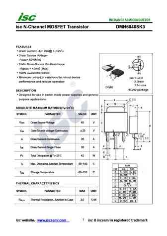
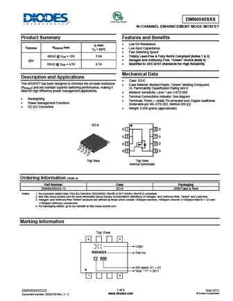
isc N-Channel MOSFET Transistor DMN6040SK3 FEATURES Drain Current I = 20A@ T =25 D C Drain Source Voltage- V = 60V(Min) DSS Static Drain-Source On-Resistance R = 40m (Max) DS(on) 100% avalanche tested Minimum Lot-to-Lot variations for robust device performance and reliable operation DESCRIPTION Designed for use in switch mode power supplies and general purp... See More ⇒
dmn6040sk3-13.pdf
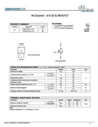
DMN6040SK3-13 www.VBsemi.tw N-Channel 6 0-V (D-S) MOSFET FEATURES PRODUCT SUMMARY TrenchFET Power MOSFET VDS (V) rDS(on) ( ) ID (A)a Available 175 C Junction Temperature 0.025 at VGS = 10 V 35 RoHS* 60 0.030 at VGS = 4.5 V 30 COMPLIANT TO-252 D G Drain Connected to Tab G D S S Top View N-Channel MOSFET ABSOLUTE MAXIMUM RATINGS TC = 25 C, unless otherwi... See More ⇒
dmn6040ssd.pdf
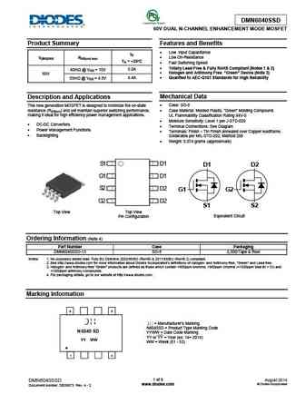
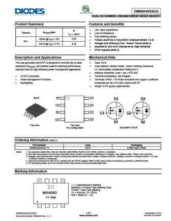
DMN6040SSD 60V DUAL N-CHANNEL ENHANCEMENT MODE MOSFET Product Summary Features and Benefits Low Input Capacitance ID Low On-Resistance V(BR)DSS RDS(on) max TA = +25 C Fast Switching Speed Totally Lead-Free & Fully RoHS Compliant (Notes 1 & 2) 40m @ VGS = 10V 5.0A Halogen and Antimony Free. Green Device (Note 3) 60V 4.4A Qualified to AEC... See More ⇒
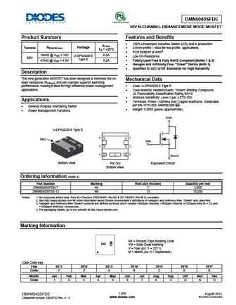
Detailed specifications: DMN53D0LW, DMN53D0U, DMN5L06-7, DMN5L06DMKQ, DMN5L06T-7, DMN5L06W-7, DMN6013LFG, DMN6040SFDE, IRFB7545, DMN6040SSD, DMN6040SSS, DMN6040SVT, DMN6069SE, DMN6070SFCL, DMN6070SSD, DMN6075S, DMN6140L
Keywords - DMN6040SK3 MOSFET specs
DMN6040SK3 cross reference
DMN6040SK3 equivalent finder
DMN6040SK3 pdf lookup
DMN6040SK3 substitution
DMN6040SK3 replacement
Learn how to find the right MOSFET substitute. A guide to cross-reference, check specs and replace MOSFETs in your circuits.
History: SDF120JDA-U | NVMFS5C466N | DMP2006UFG | HSBB3072 | SQ2361ES
🌐 : EN ES РУ

LIST
Last Update
MOSFET: FTF30P35D | FTF25N35DHVT | FTF15N35D | FTE15C35G | FTP02P15G | FTE02P15G | AKF30N5P0SX | AKF30N10S | AKF20P45D | CM4407
Popular searches
ecg123a | irfp360 | bc108 equivalent | irfp4568 | mj15004 | ksc2073 | nte102a | tip31cg