TK12A50W Specs and Replacement
Type Designator: TK12A50W
Type of Transistor: MOSFET
Type of Control Channel: N-Channel
Absolute Maximum Ratings
Pd ⓘ - Maximum Power Dissipation: 35 W
|Vds|ⓘ - Maximum Drain-Source Voltage: 500 V
|Vgs|ⓘ - Maximum Gate-Source Voltage: 30 V
|Id| ⓘ - Maximum Drain Current: 11.5 A
Tj ⓘ - Maximum Junction Temperature: 150 °C
Electrical Characteristics
tr ⓘ - Rise Time: 23 nS
Cossⓘ - Output Capacitance: 23 pF
RDSonⓘ - Maximum Drain-Source On-State Resistance: 0.3 Ohm
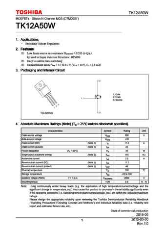
Package: TO-220F
TK12A50W substitution
- MOSFET ⓘ Cross-Reference Search
TK12A50W datasheet
tk12a50w.pdf
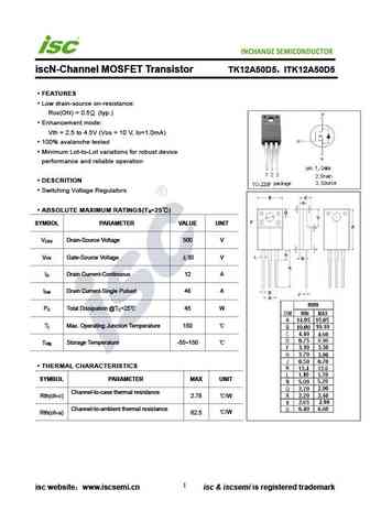
TK12A50W MOSFETs Silicon N-Channel MOS (DTMOS ) TK12A50W TK12A50W TK12A50W TK12A50W 1. Applications 1. Applications 1. Applications 1. Applications Switching Voltage Regulators 2. Features 2. Features 2. Features 2. Features (1) Low drain-source on-resistance RDS(ON) = 0.265 (typ.) by used to Super Junction Structure DTMOS (2) Easy to control Gate switching (3) E... See More ⇒
tk12a50d5.pdf
TK12A50D5 MOSFETs Silicon N-Channel MOS ( -MOS ) TK12A50D5 TK12A50D5 TK12A50D5 TK12A50D5 1. Applications 1. Applications 1. Applications 1. Applications Switching Voltage Regulators 2. Features 2. Features 2. Features 2. Features (1) Fast reverse recovery time trrf = 50 ns (typ.), trr = 120 ns (typ.) (2) Low drain-source on-resistance RDS(ON) = 0.5 (typ.) (3) High ... See More ⇒
tk12a50d.pdf
TK12A50D TOSHIBA Field Effect Transistor Silicon N Channel MOS Type ( -MOS ) TK12A50D Switching Regulator Applications Unit mm Low drain-source ON-resistance RDS (ON) = 0.45 (typ.) High forward transfer admittance Yfs = 6.0 S (typ.) Low leakage current IDSS = 10 A (max) (VDS = 500 V) Enhancement mode Vth = 2.0 to 4.0 V (VDS = 10 V, ID = 1 mA) Abs... See More ⇒
Detailed specifications: IRL40B215, IRL60B216, IRL8114, TK10A50W, TK10A60D5, TK10A80W, TK10E80W, TK12A50D5, IRF640, TK12A80W, TK17A65W, TK17A65W5, TK17E80W, TK19A50W, TK22A65X5, TK290A60Y, TK290A65Y
Keywords - TK12A50W MOSFET specs
TK12A50W cross reference
TK12A50W equivalent finder
TK12A50W pdf lookup
TK12A50W substitution
TK12A50W replacement
Can't find your MOSFET? Learn how to find a substitute transistor by analyzing voltage, current and package compatibility
🌐 : EN ES РУ

LIST
Last Update
MOSFET: ASU70R600E | ASU65R850E | ASU65R550E | ASU65R350E | ASR65R120EFD | ASR65R046EFD | ASQ65R046EFD | ASM65R280E | ASM60R330E | ASE70R950E
Popular searches
p60nf06 | 2sa1837 | ksc1845 transistor | irf630 datasheet | mpsa13 equivalent | c5198 | 2sc1969 transistor | bcy21