CED25N02 Datasheet. Specs and Replacement
Type Designator: CED25N02 📄📄
Type of Transistor: MOSFET
Type of Control Channel: N-Channel
Absolute Maximum Ratings
Pd ⓘ - Maximum Power Dissipation: 25 W
|Vds|ⓘ - Maximum Drain-Source Voltage: 20 V
|Vgs|ⓘ - Maximum Gate-Source Voltage: 10 V
|Id| ⓘ - Maximum Drain Current: 25 A
Tj ⓘ - Maximum Junction Temperature: 150 °C
Electrical Characteristics
tr ⓘ - Rise Time: 14 nS
Cossⓘ - Output Capacitance: 115 pF
RDSonⓘ - Maximum Drain-Source On-State Resistance: 0.023 Ohm
Package: TO251
📄📄 Copy
CED25N02 substitution
- MOSFET ⓘ Cross-Reference Search
CED25N02 datasheet
ced25n02 ceu25n02.pdf
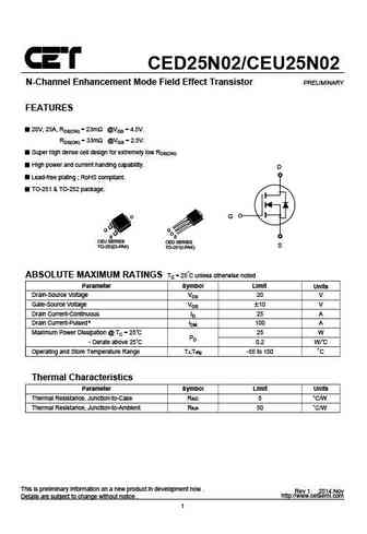
CED25N02/CEU25N02 N-Channel Enhancement Mode Field Effect Transistor PRELIMINARY FEATURES 20V, 25A, RDS(ON) = 23m @VGS = 4.5V. RDS(ON) = 33m @VGS = 2.5V. Super high dense cell design for extremely low RDS(ON). High power and current handing capability. D Lead-free plating ; RoHS compliant. TO-251 & TO-252 package. D G G S CEU SERIES CED SERIES S TO-252(D-PAK) TO-251(I-PA... See More ⇒
ceu25n15l ced25n15l.pdf
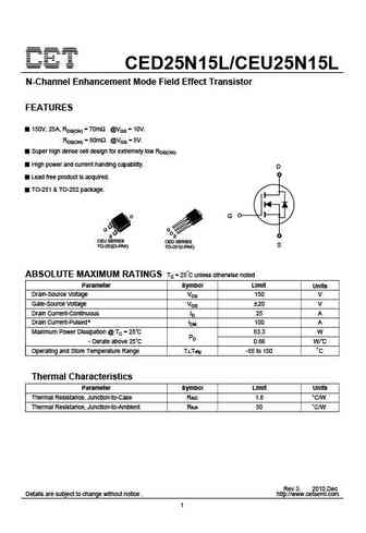
CED25N15L/CEU25N15L N-Channel Enhancement Mode Field Effect Transistor FEATURES 150V, 25A, RDS(ON) = 70m @VGS = 10V. RDS(ON) = 80m @VGS = 5V. Super high dense cell design for extremely low RDS(ON). High power and current handing capability. D Lead free product is acquired. TO-251 & TO-252 package. D G G S CEU SERIES CED SERIES S TO-252(D-PAK) TO-251(I-PAK) ABSOLUTE MAXI... See More ⇒
Detailed specifications: CJBB3139K, CJBD3020, CJBE5005, CJBM3020, CEC2088E, CEC3172, CED20N02, CEU20N02, STP80NF70, CEU25N02, CEM2192, CEM4052, CEM6056L, CEM9288, CEN2307A, CEN2321A, CEB6086
Keywords - CED25N02 MOSFET specs
CED25N02 cross reference
CED25N02 equivalent finder
CED25N02 pdf lookup
CED25N02 substitution
CED25N02 replacement
Can't find your MOSFET? Learn how to find a substitute transistor by analyzing voltage, current and package compatibility
🌐 : EN ES РУ

LIST
Last Update
MOSFET: MSH100N045SA | MSD60P16 | MSD40P45 | MSB100N023 | MS60P03 | MS40P05AU | MS40P05 | MS40N05 | MS34P07 | MS34P01
Popular searches
tip122 transistor equivalent | irfz44n equivalent | 2n2923 | 2n2102 | mj15003g | oc75 transistor | irfp260m | 2sc1213