G30N04D3 Specs and Replacement
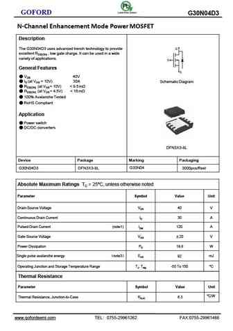
Type Designator: G30N04D3
Type of Transistor: MOSFET
Type of Control Channel: N-Channel
Absolute Maximum Ratings
Pd ⓘ - Maximum Power Dissipation: 19.8 W
|Vds|ⓘ - Maximum Drain-Source Voltage: 40 V
|Vgs|ⓘ - Maximum Gate-Source Voltage: 20 V
|Id| ⓘ - Maximum Drain Current: 30 A
Tj ⓘ - Maximum Junction Temperature: 150 °C
Electrical Characteristics
tr ⓘ - Rise Time: 17.2 nS
Cossⓘ - Output Capacitance: 209 pF
RDSonⓘ - Maximum Drain-Source On-State Resistance: 0.0095 Ohm
Package: DFN3X3-8L
G30N04D3 substitution
- MOSFET ⓘ Cross-Reference Search
G30N04D3 datasheet
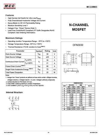
mcg30n03-tp.pdf
MCG30N03 Features High Density Cell Desihn for Ultra Low RDS(on) Fully Characterized Avalanche Voltage and Current Epoxy Meets UL 94 V-0 Flammability Rating Moisture Sensitivity Level 1 N-CHANNEL Halogen Free. Green Device (Note 1) MOSFET Lead Free Finish/RoHS Compliant ("P" Suffix Designates RoHS Compliant. See Ordering Information) Maximum Ratings ... See More ⇒
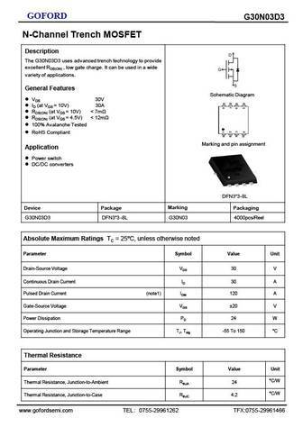
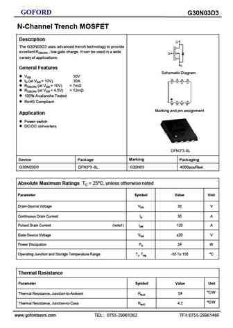
g30n03d3.pdf
GOFORD G30N03D3 N-Channel Trench MOSFET Description The G30N03D3 uses advanced trench technology to provide excellent RDS(ON) , low gate charge. It can be used in a wide variety of applications. General Features Schematic Diagram VDS 30V ID (at VGS = 10V) 30A RDS(ON) (at VGS = 10V) ... See More ⇒
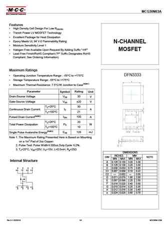
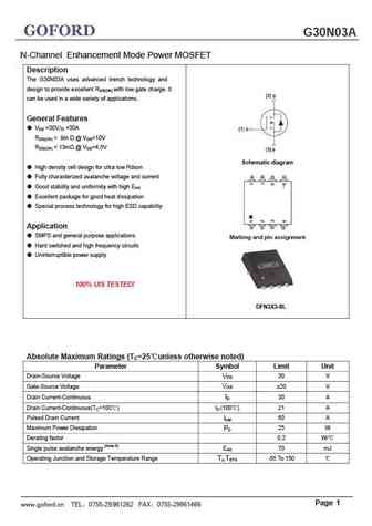
mcg30n03a.pdf
MCG30N03A Features High Density Cell Design For Low RDS(ON) Trench Power LV MOSFET Technology Excellent Package for Heat Dissipation Epoxy Meets UL 94 V-0 Flammability Rating N-CHANNEL Moisture Sensitivity Level 1 Halogen Free Available Upon Request By Adding Suffix "-HF" MOSFET Lead Free Finish/RoHS Compliant ("P" Suffix Designates RoHS Compliant. See Ord... See More ⇒
Detailed specifications: G16P03S, G18N20K, G1NP02ELL, G2003A, G20N06J, G3035-23, G30N03A, G30N03D3, 18N50, G30N20K, G30N20T, G30N20F, G33N03D3, G48N03D3, G4N60K, G50N03A, G50N03K
Keywords - G30N04D3 MOSFET specs
G30N04D3 cross reference
G30N04D3 equivalent finder
G30N04D3 pdf lookup
G30N04D3 substitution
G30N04D3 replacement
Learn how to find the right MOSFET substitute. A guide to cross-reference, check specs and replace MOSFETs in your circuits.
History: WMQ35P02TS | R6004ENJ | SVF10N65F | S2N7002DW | AOTF8T50P | 2SK2633LS | JMSH0602AGQ
🌐 : EN ES РУ
LIST
Last Update
MOSFET: AUB062N08BG | AUB060N08AG | AUB056N10 | AUB056N08BGL | AUB050N085 | AUB050N055 | AUB045N12 | AUB045N10BT | AUB039N10 | AUB034N10
Popular searches
pk6d0ba mosfet | 2sd726 | c536 transistor equivalent | 2sa1294 datasheet | mp10b transistor | bc182b | 2n3054 transistor equivalent | 2n554
