DMJ70H900HJ3 Datasheet. Specs and Replacement
Type Designator: DMJ70H900HJ3 📄📄
Type of Transistor: MOSFET
Type of Control Channel: N-Channel
Absolute Maximum Ratings
Pd ⓘ - Maximum Power Dissipation: 68 W
|Vds|ⓘ - Maximum Drain-Source Voltage: 700 V
|Vgs|ⓘ - Maximum Gate-Source Voltage: 30 V
|Id| ⓘ - Maximum Drain Current: 7 A
Tj ⓘ - Maximum Junction Temperature: 150 °C
Electrical Characteristics
tr ⓘ - Rise Time: 18.7 nS
Cossⓘ - Output Capacitance: 230 pF
RDSonⓘ - Maximum Drain-Source On-State Resistance: 0.9 Ohm
Package: TO251
📄📄 Copy
DMJ70H900HJ3 substitution
- MOSFET ⓘ Cross-Reference Search
DMJ70H900HJ3 datasheet
..1. Size:627K diodes
dmj70h900hj3.pdf 
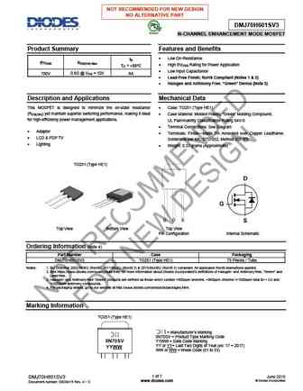
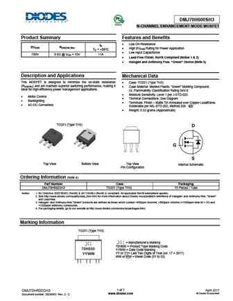
NOT RECOMMENDED FOR NEW DESIGN - DMJ70H900HJ3 NO ALTERNATE PART Green N-CHANNEL ENHANCEMENT MODE MOSFET Product Summary Features and Benefits ID Max Low On-Resistance BVDSS RDS(ON) Max TC = +25 C High BVDSS Rating for Power Application 700V 0.9 @ VGS = 10V 7A Low Input Capacitance Lead-Free Finish; RoHS Compliant (Notes 1 & 2) Halogen and Antimon... See More ⇒
..2. Size:275K inchange semiconductor
dmj70h900hj3.pdf
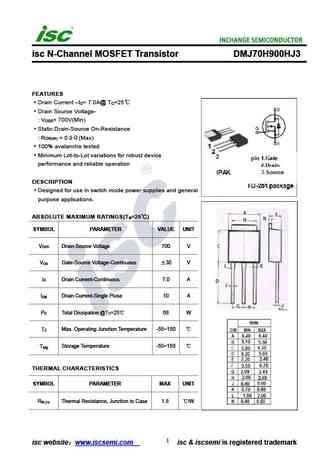
isc N-Channel MOSFET Transistor DMJ70H900HJ3 FEATURES Drain Current I = 7.0A@ T =25 D C Drain Source Voltage- V = 700V(Min) DSS Static Drain-Source On-Resistance R = 0.9 (Max) DS(on) 100% avalanche tested Minimum Lot-to-Lot variations for robust device performance and reliable operation DESCRIPTION Designed for use in switch mode power supplies and general ... See More ⇒
8.1. Size:494K diodes
dmj70h1d0sv3.pdf
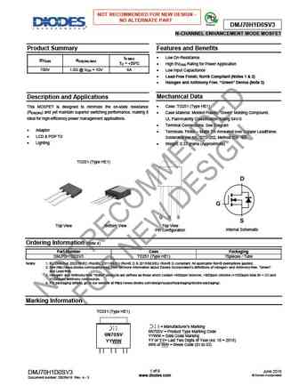
NOT RECOMMENDED FOR NEW DESIGN - NO ALTERNATE PART DMJ70H1D0SV3 N-CHANNEL ENHANCEMENT MODE MOSFET Product Summary Features and Benefits ID MAX Low On-Resistance BVDSS RDS(ON) MAX TC = +25 C High BVDSS Rating for Power Application 700V 1.0 @ VGS = 10V 6A Low Input Capacitance Lead-Free Finish; RoHS Compliant (Notes 1 & 2) Halogen and Antimony Free.... See More ⇒
8.2. Size:453K diodes
dmj70h600sh3.pdf
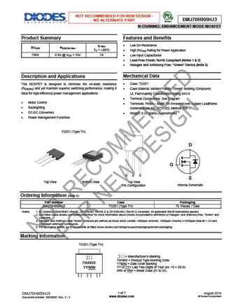
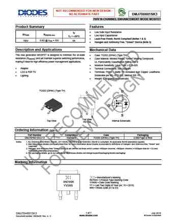
DMJ70H600SH3 N-CHANNEL ENHANCEMENT MODE MOSFET Product Summary Features and Benefits Low On-Resistance ID BVDSS RDS(ON) Max High BVDSS Rating for Power Application TC = +25 C Low Input Capacitance 700V 0.6 @ VGS = 10V 11A Lead-Free Finish; RoHS Compliant (Notes 1 & 2) Halogen and Antimony Free. Green Device (Note 3) Description and Applicati... See More ⇒
8.3. Size:452K diodes
dmj70h601sk3.pdf
NOT RECOMMENDED FOR NEW DESIGN - NO ALTERNATE PART DMJ70H601SK3 700V N-CHANNEL ENHANCEMENT MODE MOSFET Product Summary Features Low Gate Input Resistance ID BVDSS RDS(ON) max Low Input Capacitance TC = +25 C Lead-Free Finish; RoHS Compliant (Notes 1 & 2) 700V 0.6 @ VGS = 10V 8A Halogen and Antimony Free. Green Device (Note 3) Description and A... See More ⇒
8.5. Size:493K diodes
dmj70h1d5sv3.pdf
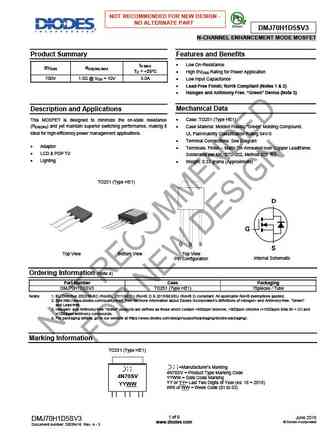
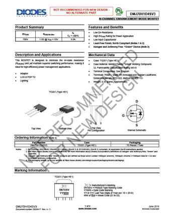
NOT RECOMMENDED FOR NEW DESIGN - NO ALTERNATE PART DMJ70H1D5SV3 N-CHANNEL ENHANCEMENT MODE MOSFET Product Summary Features and Benefits ID MAX Low On-Resistance BVDSS RDS(ON) MAX TC = +25 C High BVDSS Rating for Power Application 700V 1.5 @ VGS = 10V 5.0A Low Input Capacitance Lead-Free Finish; RoHS Compliant (Notes 1 & 2) Halogen and Antimony Fre... See More ⇒
8.7. Size:506K diodes
dmj70h1d3sh3.pdf
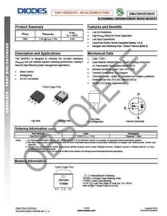
PART OBSOLETE - NO ALTERNATE PART DMJ70H1D3SH3 N-CHANNEL ENHANCEMENT MODE MOSFET Product Summary Features and Benefits ID MAX Low On-Resistance BVDSS RDS(ON) MAX TC = +25 C High BVDSS Rating for Power Application 700V 1.3 @ VGS = 10V 4.6A Low Input Capacitance Lead-Free Finish; RoHS Compliant (Notes 1 & 2) Halogen and Antimony Free. Green Devi... See More ⇒
8.8. Size:274K inchange semiconductor
dmj70h1d0sv3.pdf

isc N-Channel MOSFET Transistor DMJ70H1D0SV3 FEATURES Drain Current I = 6.0A@ T =25 D C Drain Source Voltage- V = 700V(Min) DSS Static Drain-Source On-Resistance R = 1.0 (Max) DS(on) 100% avalanche tested Minimum Lot-to-Lot variations for robust device performance and reliable operation DESCRIPTION Designed for use in switch mode power supplies and general ... See More ⇒
8.9. Size:274K inchange semiconductor
dmj70h600sh3.pdf

isc N-Channel MOSFET Transistor DMJ70H600SH3 FEATURES Drain Current I = 11A@ T =25 D C Drain Source Voltage- V = 700V(Min) DSS Static Drain-Source On-Resistance R = 0.6 (Max) DS(on) 100% avalanche tested Minimum Lot-to-Lot variations for robust device performance and reliable operation DESCRIPTION Designed for use in switch mode power supplies and general p... See More ⇒
8.10. Size:266K inchange semiconductor
dmj70h601sk3.pdf
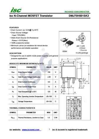
isc N-Channel MOSFET Transistor DMJ70H601SK3 FEATURES Drain Current I = 8.0A@ T =25 D C Drain Source Voltage- V = 700V(Min) DSS Static Drain-Source On-Resistance R = 0.6 (Max) DS(on) 100% avalanche tested Minimum Lot-to-Lot variations for robust device performance and reliable operation DESCRIPTION Designed for use in switch mode power supplies and general ... See More ⇒
8.11. Size:274K inchange semiconductor
dmj70h601sv3.pdf

isc N-Channel MOSFET Transistor DMJ70H601SV3 FEATURES Drain Current I = 8.0A@ T =25 D C Drain Source Voltage- V = 700V(Min) DSS Static Drain-Source On-Resistance R = 0.6 (Max) DS(on) 100% avalanche tested Minimum Lot-to-Lot variations for robust device performance and reliable operation DESCRIPTION Designed for use in switch mode power supplies and general ... See More ⇒
8.12. Size:274K inchange semiconductor
dmj70h1d5sv3.pdf

isc N-Channel MOSFET Transistor DMJ70H1D5SV3 FEATURES Drain Current I = 5.0A@ T =25 D C Drain Source Voltage- V = 700V(Min) DSS Static Drain-Source On-Resistance R = 1.5 (Max) DS(on) 100% avalanche tested Minimum Lot-to-Lot variations for robust device performance and reliable operation DESCRIPTION Designed for use in switch mode power supplies and general ... See More ⇒
8.13. Size:274K inchange semiconductor
dmj70h1d4sv3.pdf

isc N-Channel MOSFET Transistor DMJ70H1D4SV3 FEATURES Drain Current I = 5.0A@ T =25 D C Drain Source Voltage- V = 700V(Min) DSS Static Drain-Source On-Resistance R = 1.5 (Max) DS(on) 100% avalanche tested Minimum Lot-to-Lot variations for robust device performance and reliable operation DESCRIPTION Designed for use in switch mode power supplies and general ... See More ⇒
8.14. Size:273K inchange semiconductor
dmj70h1d3sh3.pdf

isc N-Channel MOSFET Transistor DMJ70H1D3SH3 FEATURES Drain Current I = 4.6A@ T =25 D C Drain Source Voltage- V = 700V(Min) DSS Static Drain-Source On-Resistance R = 1.3 (Max) DS(on) 100% avalanche tested Minimum Lot-to-Lot variations for robust device performance and reliable operation DESCRIPTION Designed for use in switch mode power supplies and general ... See More ⇒
Detailed specifications: DMG8N65SCT, DMJ70H1D0SV3, DMJ70H1D3SH3, DMJ70H1D4SV3, DMJ70H1D5SV3, DMJ70H600SH3, DMJ70H601SK3, DMJ70H601SV3, 75N75, DMN15H310SK3, DMN6017SK3, DMN60H3D5SK3, DMN60H4D5SK3, DMN80H2D0SCTI, DMN90H2D2HCTI, DMN90H8D5HCT, DMN90H8D5HCTI
Keywords - DMJ70H900HJ3 MOSFET specs
DMJ70H900HJ3 cross reference
DMJ70H900HJ3 equivalent finder
DMJ70H900HJ3 pdf lookup
DMJ70H900HJ3 substitution
DMJ70H900HJ3 replacement
Can't find your MOSFET?
Learn how to find a substitute transistor by analyzing voltage, current and package compatibility