HYG110P04LQ2D Datasheet. Specs and Replacement
Type Designator: HYG110P04LQ2D
Type of Transistor: MOSFET
Type of Control Channel: P-Channel
Absolute Maximum Ratings
Pd ⓘ - Maximum Power Dissipation: 57.7 W
|Vds|ⓘ - Maximum Drain-Source Voltage: 40 V
|Vgs|ⓘ - Maximum Gate-Source Voltage: 20 V
|Id| ⓘ - Maximum Drain Current: 50 A
Tj ⓘ - Maximum Junction Temperature: 175 °C
Electrical Characteristics
tr ⓘ - Rise Time: 48 nS
Cossⓘ - Output Capacitance: 253 pF
RDSonⓘ - Maximum Drain-Source On-State Resistance: 0.012 Ohm
Package: TO252
HYG110P04LQ2D substitution
- MOSFET ⓘ Cross-Reference Search
HYG110P04LQ2D datasheet
hyg110p04lq2d hyg110p04lq2u hyg110p04lq2v.pdf
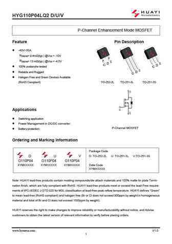
HYG110P04LQ2 D/U/V P-Channel Enhancement Mode MOSFET Feature Pin Description -40V/-50A RDS(ON)= 9.4m (typ.) @VGS = -10V RDS(ON)= 13 m (typ.) @VGS = -4.5V S D S G D 100% avalanche tested G S Reliable and Rugged D G Halogen Free and Green Devices Available (RoHS Compliant) TO-252-2L TO-251-3L TO-251-3S Applications Switching application Power Management in ... See More ⇒
hyg110p04lq2c2.pdf
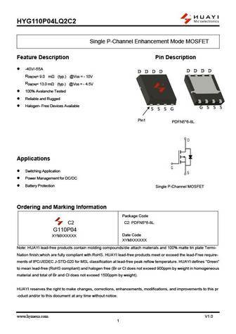
HYG110P04LQ2C2 Single P-Channel Enhancement Mode MOSFET Feature Description Pin Description -40V/-55A D D D D D D D D RDS(ON)= 9.0 m (typ.) @VGS = - 10V RDS(ON)= 13.0 m (typ.) @VGS = - 4.5V 100% Avalanche Tested Reliable and Rugged Halogen- Free Devices Available G S S S S S S G Pin1 PDFN5*6-8L Applications Switching Application Powe... See More ⇒
Detailed specifications: HYG065N07NS1B, HYG065N15NS1B6, HYG065N15NS1P, HYG065N15NS1B, HYG068N08NR1P, HYG080N10LS1D, HYG082N03LR1C1, HYG092N10LS1C2, 8N60, HYG110P04LQ2U, HYG110P04LQ2V, HYG210P06LQ1D, HYG210P06LQ1U, HYG210P06LQ1V, HYG400P10LR1D, HYG400P10LR1U, HYG400P10LR1V
Keywords - HYG110P04LQ2D MOSFET specs
HYG110P04LQ2D cross reference
HYG110P04LQ2D equivalent finder
HYG110P04LQ2D pdf lookup
HYG110P04LQ2D substitution
HYG110P04LQ2D replacement
Step-by-step guide to finding a MOSFET replacement. Cross-reference parts and ensure compatibility for your repair or project.
🌐 : EN ES РУ

LIST
Last Update
MOSFET: FTF30P35D | FTF25N35DHVT | FTF15N35D | FTE15C35G | FTP02P15G | FTE02P15G | AKF30N5P0SX | AKF30N10S | AKF20P45D | CM4407
Popular searches
2n3906 equivalent | a733 transistor equivalent | 2n5401 transistor datasheet | 2n2222 data sheet | irf3205 datasheet | oc71 | njw0302g | 2n3904 transistor equivalent