BSC110N15NS5 Specs and Replacement
Type Designator: BSC110N15NS5
Type of Transistor: MOSFET
Type of Control Channel: N-Channel
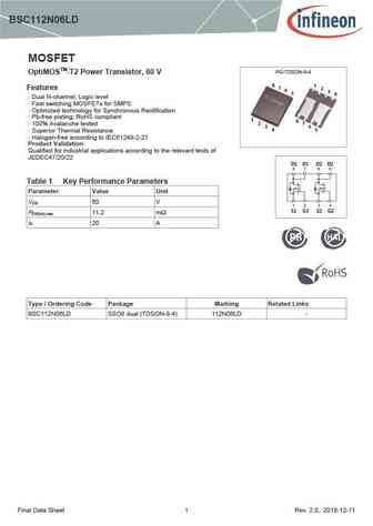
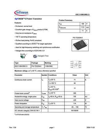
Absolute Maximum Ratings
Pd ⓘ - Maximum Power Dissipation: 2.5 W
|Vds|ⓘ - Maximum Drain-Source Voltage: 150 V
|Vgs|ⓘ - Maximum Gate-Source Voltage: 20 V
|Id| ⓘ - Maximum Drain Current: 12 A
Tj ⓘ - Maximum Junction Temperature: 150 °C
Electrical Characteristics
tr ⓘ - Rise Time: 3.3 nS
Cossⓘ - Output Capacitance: 515 pF
RDSonⓘ - Maximum Drain-Source On-State Resistance: 0.011 Ohm
Package: SUPERSO8
BSC110N15NS5 substitution
- MOSFET ⓘ Cross-Reference Search
BSC110N15NS5 datasheet
bsc110n15ns5.pdf

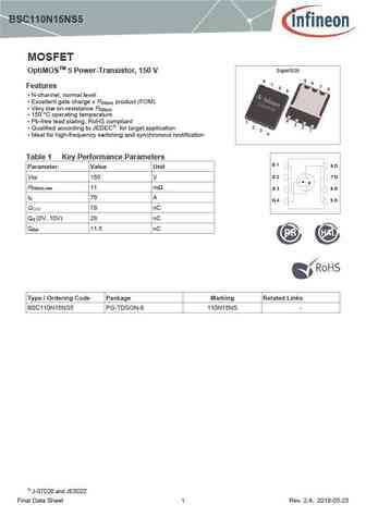
BSC110N15NS5 MOSFET SuperSO8 OptiMOSTM 5 Power-Transistor, 150 V 5 8 6 7 Features 7 6 8 5 N-channel, normal level Excellent gate charge x R product (FOM) DS(on) Very low on-resistance R DS(on) 150 C operating temperature 4 Pb-free lead plating; RoHS compliant 1 3 2 2 Qualified according to JEDEC1) for target application 3 1 4 Ideal for hig... See More ⇒
bsc110n15ns5.pdf
BSC110N15NS5 MOSFET SuperSO8 OptiMOSTM 5 Power-Transistor, 150 V 5 8 6 7 Features 7 6 8 5 N-channel, normal level Excellent gate charge x R product (FOM) DS(on) Very low on-resistance R DS(on) 150 C operating temperature 4 Pb-free lead plating; RoHS compliant 1 3 2 2 Qualified according to JEDEC1) for target application 3 1 4 Ideal for hig... See More ⇒
bsc110n06ns3g.pdf
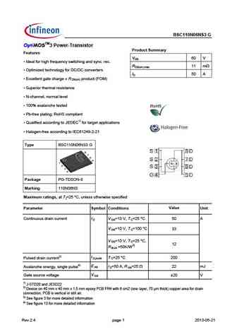
Type BSC110N06NS3 G OptiMOSTM3 Power-Transistor Product Summary Features VDS 60 V Ideal for high frequency switching and sync. rec. RDS(on),max 11 mW Optimized technology for DC/DC converters ID 50 A Excellent gate charge x R product (FOM) DS(on) Superior thermal resistance N-channel, normal level 100% avalanche tested Pb-free plating; RoHS compl... See More ⇒
bsc110n06ns3.pdf
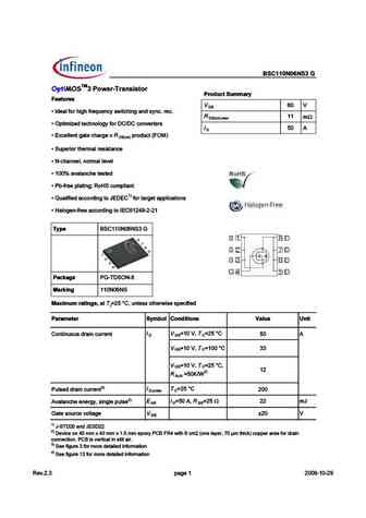
pe $ $ TM "9@/; %;+877+;B Features V D Q #4513I CG9D389>7 1>4 CI>3 B53 R 11 m D n) m x Q ( @D9=9J54 D538>?F5BD5BC I D Q H35>5?B=1... See More ⇒
Detailed specifications: BSC0804LS, BSC0805LS, BSC093N15NS5, BSC094N06LS5, BSC096N10LS5, BSC097N06NST, BSC0993ND, BSC0996NS, IRFZ44N, BSC112N06LD, BSC13DN30NSFD, BSC146N10LS5, BSC155N06ND, BSC160N15NS5, BSC350N20NSFD, BSF450NE7NH3G, BSS340NW
Keywords - BSC110N15NS5 MOSFET specs
BSC110N15NS5 cross reference
BSC110N15NS5 equivalent finder
BSC110N15NS5 pdf lookup
BSC110N15NS5 substitution
BSC110N15NS5 replacement
Learn how to find the right MOSFET substitute. A guide to cross-reference, check specs and replace MOSFETs in your circuits.
History: SI1307EDL | FDP8870F085 | STK900 | SNN0310Q
🌐 : EN ES РУ

LIST
Last Update
MOSFET: AUB034N10 | AUB033N08BG | AUB026N085 | AUA062N08BG | AUA060N08AG | AUA056N08BGL | AUA039N10 | ASW80R290E | ASW65R120EFD | ASW65R110E
Popular searches
2sa722 | f1010e mosfet datasheet | 2sa566 | bc559 equivalent | c2075 transistor | ecg123 | 2n5551 transistor equivalent | 13009 datasheet