3415E Specs and Replacement
Type Designator: 3415E
Type of Transistor: MOSFET
Type of Control Channel: N-Channel
Absolute Maximum Ratings
Pd ⓘ - Maximum Power Dissipation: 0.3 W
|Vds|ⓘ - Maximum Drain-Source Voltage: 9 V
|Vgs|ⓘ - Maximum Gate-Source Voltage: 6 V
|Id| ⓘ - Maximum Drain Current: 3.5 A
Tj ⓘ - Maximum Junction Temperature: 150 °C
Electrical Characteristics
RDSonⓘ - Maximum Drain-Source On-State Resistance: 0.06 Ohm
Package: SOT23
3415E substitution
- MOSFET ⓘ Cross-Reference Search
3415E datasheet
3415e.pdf
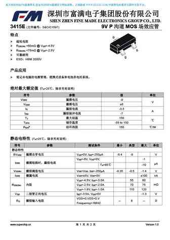
FM , FM WWW.SZLCSC.COM, SHEN ZHEN FINE MADE ELECTRONICS GROUP CO., LTD. 3415E ( S&CIC1597) 9V P MOS R ... See More ⇒
lp3415elt1g s-lp3415elt1g.pdf
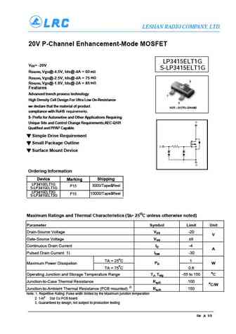
LESHAN RADIO COMPANY, LTD. 20V P-Channel Enhancement-Mode MOSFET LP3415ELT1G V = -20V DS S-LP3415ELT1G R Vgs@-4.5V, Ids@-4A = 60 m DS(ON), m R DS(ON), Vgs@-2.5V, Ids@-4A = 75 3 m RDS(ON), Vgs@-1.8V, Ids@-2A = 85 Features Advanced trench process technology 1 High Density Cell Design For Ultra Low On-Resistance 2 we declare that the material of product SOT 23 (... See More ⇒
mmp3415e.pdf
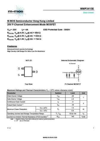
MMP3415E Data Sheet M-MOS Semiconductor Hong Kong Limited 20V P-Channel Enhancement-Mode MOSFET VDS= -20V ID= -4A ESD Protected Gate 3000V RDS(ON), Vgs@-4.5V, Ids@-4A = 55m RDS(ON), Vgs@-2.5V, Ids@-4A = 63m RDS(ON), Vgs@-1.8V, Ids@-2A = 73m Features Advanced trench process technology High Density Cell Design For Ultra Low On-Resistance SOT-23 Internal Schematic Diagram To... See More ⇒
nce3415e.pdf
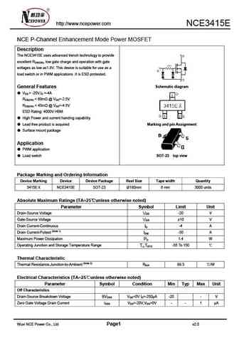
http //www.ncepower.com NCE3415E NCE P-Channel Enhancement Mode Power MOSFET Description The NCE3415E uses advanced trench technology to provide excellent RDS(ON), low gate charge and operation with gate voltages as low as1.8V. This device is suitable for use as a load switch or in PWM applications .It is ESD protested. Schematic diagram General Features VDS = -20V,ID =-4... See More ⇒
Detailed specifications: .8205P, 2060K., 2301P, 2302P, 3050K, 3060K, 3080K, 3090K, 75N75, 4080K, 6888K, SC8205, SC8205S, PDNM6ET20V05, PNM3FD201E0, PNM3FD20V1E, PNM523T30V01
Keywords - 3415E MOSFET specs
3415E cross reference
3415E equivalent finder
3415E pdf lookup
3415E substitution
3415E replacement
Need a MOSFET replacement? Our guide shows you how to find a perfect substitute by comparing key parameters and specs
🌐 : EN ES РУ

LIST
Last Update
MOSFET: AUB034N10 | AUB033N08BG | AUB026N085 | AUA062N08BG | AUA060N08AG | AUA056N08BGL | AUA039N10 | ASW80R290E | ASW65R120EFD | ASW65R110E
Popular searches
bdw94c | bd140 transistor | 2n2222a datasheet | bd136 | tl431 datasheet | 2sd526 | 2n4403 transistor equivalent | 2sc1318