APM4532KC Specs and Replacement
Type Designator: APM4532KC
Type of Transistor: MOSFET
Type of Control Channel: NP-Channel
Absolute Maximum Ratings
Pd ⓘ - Maximum Power Dissipation: 2 W
|Vds|ⓘ - Maximum Drain-Source Voltage: 30 V
|Vgs|ⓘ - Maximum Gate-Source Voltage: 20 V
|Id| ⓘ - Maximum Drain Current: 6.8 A
Tj ⓘ - Maximum Junction Temperature: 150 °C
Electrical Characteristics
tr ⓘ - Rise Time: 11 nS
Cossⓘ - Output Capacitance: 95 pF
RDSonⓘ - Maximum Drain-Source On-State Resistance: 0.018 typ Ohm
Package: SO8
APM4532KC substitution
- MOSFET ⓘ Cross-Reference Search
APM4532KC datasheet
apm4532kc.pdf
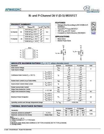
APM4532KC www.VBsemi.tw N- and P-Channel 30 V (D-S) MOSFET FEATURES PRODUCT SUMMARY Halogen-free According to IEC 61249-2-21 VDS (V) RDS(on) ( ) Definition ID (A)a Qg (Typ.) TrenchFET Power MOSFET 0.018 at VGS = 10 V 8e 100 % Rg and UIS Tested N-Channel 30 0.020 at VGS = 8 V 8e 6.2 Compliant to RoHS Directive 2002/95/EC 0.024 at VGS = 4.5 V 8e 0.032 at VG... See More ⇒
apm4532k.pdf

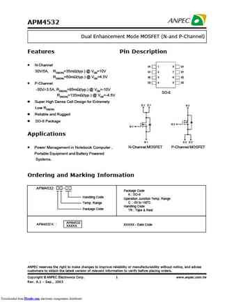
APM4532K Dual Enhancement Mode MOSFET (N-and P-Channel) Features Pin Description N-Channel D1 D1 D2 30V/5A, D2 RDS(ON) =35m (typ.) @ VGS = 10V S1 RDS(ON) =60m (typ.) @ VGS = 4.5V G1 S2 G2 P-Channel -30V/-3.5A, Top View of SOP - 8 RDS(ON) =85m (typ.) @ VGS =-10V (8) (7) (3) RDS(ON) =135m (typ.) @ VGS =-4.5V D1 D1 S2 Super High Dense C... See More ⇒
apm4532.pdf
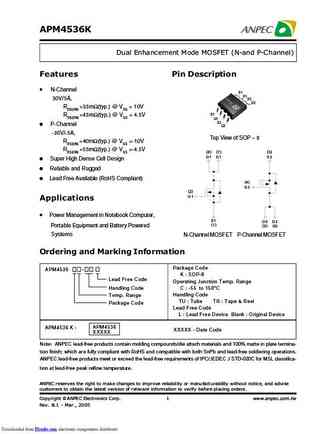
APM4532 Dual Enhancement Mode MOSFET (N-and P-Channel) Features Pin Description N-Channel S1 1 8 D1 30V/5A, RDS(ON)=35m (typ.) @ VGS=10V G1 2 7 D1 RDS(ON)=60m (typ.) @ VGS=4.5V S2 3 6 D2 G2 4 5 D2 P-Channel -30V/-3.5A, RDS(ON)=85m (typ.) @ VGS=-10V SO-8 RDS(ON)=135m (typ.) @ VGS=-4.5V Super High Dense Cell Design for Extremely D1 D1 S2 Lo... See More ⇒
apm4536k.pdf
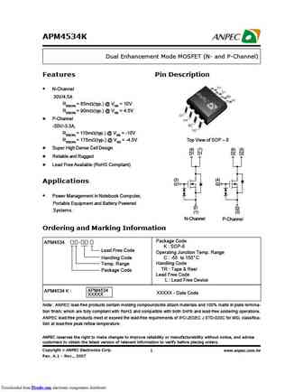
APM4536K Dual Enhancement Mode MOSFET (N-and P-Channel) Features Pin Description N-Channel D1 D1 30V/5A, D2 D2 RDS(ON) =35m (typ.) @ VGS = 10V S1 RDS(ON) =45m (typ.) @ VGS = 4.5V G1 S2 P-Channel G2 -30V/-5A, Top View of SOP - 8 RDS(ON) =40m (typ.) @ VGS =-10V RDS(ON) =55m (typ.) @ VGS =-4.5V (8) (7) (3) D1 D1 S2 Super High Dense Cell ... See More ⇒

Detailed specifications: APM3040NDC, APM3054NUC, APM3055LUC, APM4010NUC, APM4050APUC, APM4050PUC, APM4303KC, APM4330KC, IRF3710, APM4550KC, APM4828KC-TRL, APM4927KC, APM4953KC, APM7313KC, APM7318KC, APM8010KC, APM9435KC
Keywords - APM4532KC MOSFET specs
APM4532KC cross reference
APM4532KC equivalent finder
APM4532KC pdf lookup
APM4532KC substitution
APM4532KC replacement
Can't find your MOSFET? Learn how to find a substitute transistor by analyzing voltage, current and package compatibility
History: APM4010NUC | STK900 | FDP8870F085
🌐 : EN ES РУ

LIST
Last Update
MOSFET: AUB034N10 | AUB033N08BG | AUB026N085 | AUA062N08BG | AUA060N08AG | AUA056N08BGL | AUA039N10 | ASW80R290E | ASW65R120EFD | ASW65R110E
Popular searches
c2389 transistor | c2634 transistor | mdp1991 datasheet | 40636 transistor | ao3407 datasheet | c1841 transistor | fb42n20d | irfb3306 equivalent