100N03A Specs and Replacement
Type Designator: 100N03A
Type of Transistor: MOSFET
Type of Control Channel: N-Channel
Absolute Maximum Ratings
Pd ⓘ - Maximum Power Dissipation: 105 W
|Vds|ⓘ - Maximum Drain-Source Voltage: 30 V
|Vgs|ⓘ - Maximum Gate-Source Voltage: 20 V
|Id| ⓘ - Maximum Drain Current: 90 A
Tj ⓘ - Maximum Junction Temperature: 150 °C
Electrical Characteristics
tr ⓘ - Rise Time: 36.4 nS
Cossⓘ - Output Capacitance: 248 pF
RDSonⓘ - Maximum Drain-Source On-State Resistance: 0.0049 Ohm
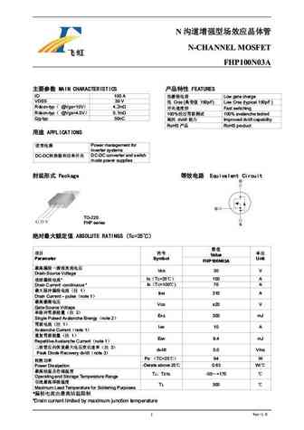
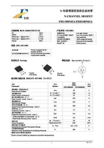
Package: TO252
100N03A substitution
- MOSFET ⓘ Cross-Reference Search
100N03A datasheet
100n03a.pdf
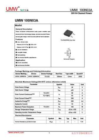
R UMW UMW 100N03A 30V N-Channel Power UMW 100N03A Mosfet General Description These N-channel enhancement mode power mosfets used advanced trench technology design, provided excellent Rdson and low gate charge. Which accords with the RoHS standard. Features VDS = 30V,ID =90A RDS(ON),3.8 m (Typ) @ VGS =10V RDS(ON), 6.4m (Typ) @ VGS =4.5V Low on resistance Low gate charge Fast s... See More ⇒
jmtg100n03a.pdf
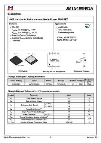
JMTG100N03A Description JMT N-channel Enhancement Mode Power MOSFET Features Applications 30V, 30A Load Switch RDS(ON) ... See More ⇒
Detailed specifications: IRLR2905TR, IRLR2905ZTR, IRLR2908TR, IRLR3105TR, IRLR3410TR, IRLR3636TRPBF, IRLR8103VTR, IRLR8729TR, IRFB4227, 30N03A, 35N06, AO3402A, AO3403A, AO3409A, AO3413A, AO3414A, AO3416A
Keywords - 100N03A MOSFET specs
100N03A cross reference
100N03A equivalent finder
100N03A pdf lookup
100N03A substitution
100N03A replacement
Need a MOSFET replacement? Our guide shows you how to find a perfect substitute by comparing key parameters and specs
History: ELM33410CA | 2SK3298
🌐 : EN ES РУ

LIST
Last Update
MOSFET: AUB034N10 | AUB033N08BG | AUB026N085 | AUA062N08BG | AUA060N08AG | AUA056N08BGL | AUA039N10 | ASW80R290E | ASW65R120EFD | ASW65R110E
Popular searches
mj15022 | toshiba c5198 | irf520n datasheet | tip107 | 2n5457 | k3568 | 2sc1344 | cs840f