SPN6561S26RGB Specs and Replacement
Type Designator: SPN6561S26RGB
Type of Transistor: MOSFET
Type of Control Channel: N-Channel
Absolute Maximum Ratings
Pd ⓘ - Maximum Power Dissipation: 1.14 W
|Vds|ⓘ - Maximum Drain-Source Voltage: 20 V
|Vgs|ⓘ - Maximum Gate-Source Voltage: 12 V
|Id| ⓘ - Maximum Drain Current: 3.5 A
Tj ⓘ - Maximum Junction Temperature: 150 °C
Electrical Characteristics
tr ⓘ - Rise Time: 15 nS
Cossⓘ - Output Capacitance: 55 pF
RDSonⓘ - Maximum Drain-Source On-State Resistance: 0.022 typ Ohm
Package: TSOP6
SPN6561S26RGB substitution
- MOSFET ⓘ Cross-Reference Search
SPN6561S26RGB datasheet
spn6561s26rgb.pdf
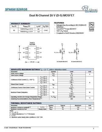
SPN6561S26RGB www.VBsemi.tw Dual N-Channel 20 V (D-S) MOSFET FEATURES PRODUCT SUMMARY Halogen-free According to IEC 61249-2-21 VDS (V) RDS(on) ( ) ID (A)a Qg (Typ.) Definition 0.022 at VGS = 4.5 V TrenchFET Power MOSFET 6.0 20 1.8 nC 100 % Rg Tested 0.028 at VGS = 2.5 V 5.0 Compliant to RoHS Directive 2002/95/EC TSOP-6 D1 D 2 D Top View G1 D1 1 6 ... See More ⇒
spn65t10.pdf
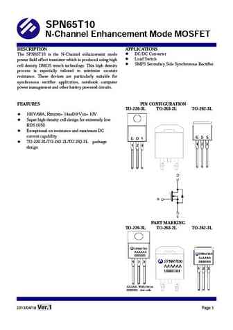
SPN65T10 N-Channel Enhancement Mode MOSFET DESCRIPTION APPLICATIONS DC/DC Converter The SPN65T10 is the N-Channel enhancement mode Load Switch power field effect transistor which is produced using high SMPS Secondary Side Synchronous Rectifier cell density DMOS trench technology. This high density process is especially tailored to minimize on-state resistance. These devic... See More ⇒
Detailed specifications: SP8K1TB, SP8M3-TB, SPD09N05, SPN2054T252RG, SPN2302S23R, SPN3414S23RGB, SPN4412WS8RG, SPN4436S8R, IRFB31N20D, SPP3414S23RG, SPP6506S26R, SPP6507S26RGB, SPP80N03S2L, SQ9407EY-T1, SSC8022GS6, SSM2307G, ST2300S23RG
Keywords - SPN6561S26RGB MOSFET specs
SPN6561S26RGB cross reference
SPN6561S26RGB equivalent finder
SPN6561S26RGB pdf lookup
SPN6561S26RGB substitution
SPN6561S26RGB replacement
Step-by-step guide to finding a MOSFET replacement. Cross-reference parts and ensure compatibility for your repair or project.
🌐 : EN ES РУ

LIST
Last Update
MOSFET: ASD80R750E | ASD70R950E | ASD70R600E | ASD70R380E | ASD65R850E | ASD65R550E | ASD65R350E | ASD65R300E | ASD65R280E | ASD65R270E
Popular searches
2sc1166 | jcs9n50fc datasheet | 2n2147 | 2sc870 | 2sa771 | d667 | a965 transistor | hy3210