FDD3672 Specs and Replacement
Type Designator: FDD3672
Type of Transistor: MOSFET
Type of Control Channel: N-Channel
Absolute Maximum Ratings
Pd ⓘ
- Maximum Power Dissipation: 135 W
|Vds|ⓘ - Maximum Drain-Source Voltage: 100 V
|Vgs|ⓘ - Maximum Gate-Source Voltage: 20 V
|Id| ⓘ - Maximum Drain Current: 44 A
Tj ⓘ - Maximum Junction Temperature: 175 °C
Electrical Characteristics
Rds ⓘ - Maximum Drain-Source On-State Resistance: 0.028 Ohm
Package: TO252
DPAK
- MOSFET ⓘ Cross-Reference Search
FDD3672 datasheet
..1. Size:268K fairchild semi
fdd3672.pdf 
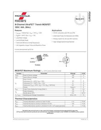
March 2010 FDD3672 N-Channel UltraFET Trench MOSFET 100V, 44A, 28m Features Applications rDS(ON) = 24m (Typ.), VGS = 10V, ID = 44A DC/DC converters and Off-Line UPS Qg(tot) = 24nC (Typ.), VGS = 10V Distributed Power Architectures and VRMs Low Miller Charge Primary Switch for 24V and 48V Systems Low Qrr Body Diode High Voltage Synchronous Rectif... See More ⇒
..2. Size:111K fairchild semi
fdd3672 f085.pdf
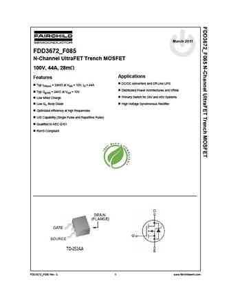
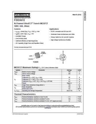
March 2011 FDD3672_F085 N-Channel UltraFET Trench MOSFET 100V, 44A, 28m Applications Features DC/DC converters and Off-Line UPS Typ rDS(on) = 24m at VGS = 10V, ID = 44A Distributed Power Architectures and VRMs Typ Qg(10) = 24nC at VGS = 10V Primary Switch for 24V and 48V Systems Low Miller Charge Low Qrr Body Diode High Voltage Synchronous Rectifier Optimized efficie... See More ⇒
..4. Size:111K onsemi
fdd3672 f085.pdf

March 2011 FDD3672_F085 N-Channel UltraFET Trench MOSFET 100V, 44A, 28m Applications Features DC/DC converters and Off-Line UPS Typ rDS(on) = 24m at VGS = 10V, ID = 44A Distributed Power Architectures and VRMs Typ Qg(10) = 24nC at VGS = 10V Primary Switch for 24V and 48V Systems Low Miller Charge Low Qrr Body Diode High Voltage Synchronous Rectifier Optimized efficie... See More ⇒
..5. Size:860K cn vbsemi
fdd3672.pdf

FDD3672 www.VBsemi.tw N-Channel 100-V (D-S) MOSFET FEATURES PRODUCT SUMMARY TrenchFET Power MOSFETS V(BR)DSS (V) rDS(on) ( )ID (A) Available 175 C Junction Temperature 0.030 at VGS = 10 V 40 RoHS* 100 Low Thermal Resistance Package 0.035 at VGS = 4.5 V 37 COMPLIANT D TO-252 G G D S Top View S N-Channel MOSFET ABSOLUTE MAXIMUM RATINGS TC = 25 C, unless... See More ⇒
8.1. Size:67K fairchild semi
fdd3670.pdf
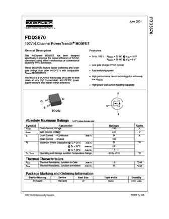
June 2001 FDD3670 100V N-Channel PowerTrench MOSFET General Description Features This N-Channel MOSFET has been designed 34 A, 100 V. R = 32 m @ V = 10 V DS(ON) GS specifically to improve the overall efficiency of DC/DC R = 35 m @ V = 6 V DS(ON) GS converters using either synchronous or conventional switching PWM controllers. Low gate charge (57 nC typical) ... See More ⇒
9.1. Size:84K fairchild semi
fdd3690.pdf
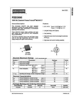
April 2001 FDD3690 100V N-Channel PowerTrench MOSFET General Description Features This N-Channel MOSFET has been designed 22 A, 100 V. RDS(ON) = 64 m @ VGS = 10 V specifically to improve the overall efficiency of DC/DC RDS(ON) = 71 m @ VGS = 6 V converters using either synchronous or conventional switching PWM controllers. Low gate charge (28nC... See More ⇒
9.2. Size:75K fairchild semi
fdd3680.pdf
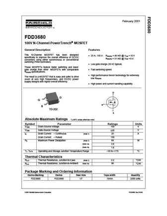
February 2001 FDD3680 100V N-Channel PowerTrench MOSFET General Description Features This N-Channel MOSFET has been designed 25 A, 100 V. R = 46 m @ V = 10 V DS(ON) GS specifically to improve the overall efficiency of DC/DC R = 51 m @ V = 6 V DS(ON) GS converters using either synchronous or conventional switching PWM controllers. Low gate charge (38 nC typical) These ... See More ⇒
9.3. Size:266K fairchild semi
fdd3682.pdf
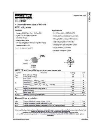
September 2002 FDD3682 N-Channel PowerTrench MOSFET 100V, 32A, 36m Features Applications rDS(ON) = 32m (Typ.), VGS = 10V, ID = 32A DC/DC converters and Off-Line UPS Qg(tot) = 18.5nC (Typ.), VGS = 10V Distributed Power Architectures and VRMs Low Miller Charge Primary Switch for 24V and 48V Systems Low QRR Body Diode High Voltage Synchronous Rect... See More ⇒
9.4. Size:254K onsemi
fdd3690.pdf
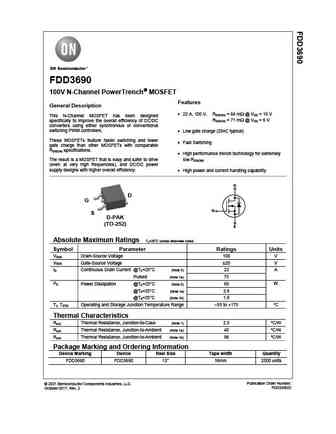
FDD3690 100V N-Channel PowerTrench MOSFET Features General Description 22 A, 100 V. RDS(ON) = 64 m @ VGS = 10 V This N-Channel MOSFET has been designed specifically to improve the overall efficiency of DC/DC RDS(ON) = 71 m @ VGS = 6 V converters using either synchronous or conventional switching PWM controllers. Low gate charge (28nC typical) The... See More ⇒
9.5. Size:389K onsemi
fdd3680.pdf
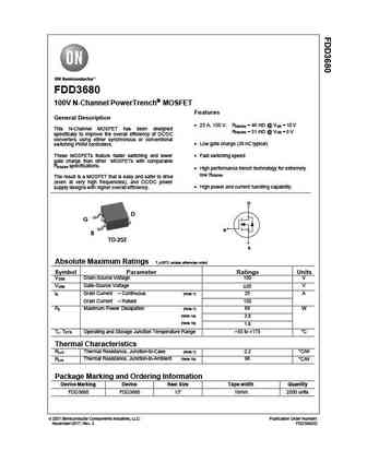
FDD3680 100V N-Channel PowerTrench MOSFET Features General Description 25 A, 100 V. R = 46 m @ V = 10 V DS(ON) GS This N-Channel MOSFET has been designed R = 51 m @ V = 6 V DS(ON) GS specifically to improve the overall efficiency of DC/DC converters using either synchronous or conventional Low gate charge (38 nC typical) switching PWM controllers. These MOSFETs featur... See More ⇒
9.6. Size:289K onsemi
fdd3682-f085.pdf
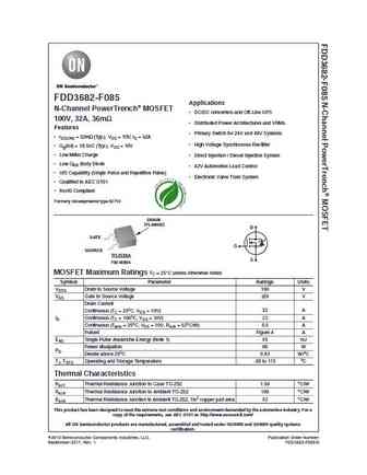
FDD3682-F085 Applications N-Channel PowerTrench MOSFET DC/DC converters and Off-Line UPS 100V, 32A, 36m Distributed Power Architectures and VRMs Features Primary Switch for 24V and 48V Systems rDS(ON) = 32m (Typ.), VGS = 10V, ID = 32A High Voltage Synchronous Rectifier Qg(tot) = 18.5nC (Typ.), VGS = 10V Low Miller Charge Direct Injection / Die... See More ⇒
9.7. Size:442K onsemi
fdd3682.pdf

Is Now Part of To learn more about ON Semiconductor, please visit our website at www.onsemi.com Please note As part of the Fairchild Semiconductor integration, some of the Fairchild orderable part numbers will need to change in order to meet ON Semiconductor s system requirements. Since the ON Semiconductor product management systems do not have the ability to manage part nomenclatur... See More ⇒
9.8. Size:819K cn vbsemi
fdd3680.pdf
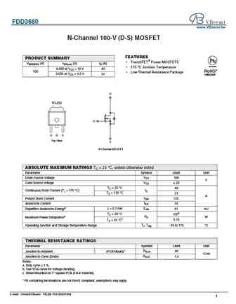
FDD3680 www.VBsemi.tw N-Channel 100-V (D-S) MOSFET FEATURES PRODUCT SUMMARY TrenchFET Power MOSFETS V(BR)DSS (V) rDS(on) ( )ID (A) Available 175 C Junction Temperature 0.030 at VGS = 10 V 40 RoHS* 100 Low Thermal Resistance Package 0.035 at VGS = 4.5 V 37 COMPLIANT D TO-252 G G D S Top View S N-Channel MOSFET ABSOLUTE MAXIMUM RATINGS TC = 25 C, unless... See More ⇒
9.9. Size:1407K cn vbsemi
fdd3682.pdf
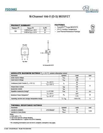
FDD3682 www.VBsemi.tw N-Channel 100-V (D-S) MOSFET FEATURES PRODUCT SUMMARY TrenchFET Power MOSFETS V(BR)DSS (V) rDS(on) ( )ID (A) Available 175 C Junction Temperature 0.030 at VGS = 10 V 40 RoHS* 100 Low Thermal Resistance Package 0.035 at VGS = 4.5 V 37 COMPLIANT D TO-252 G G D S Top View S N-Channel MOSFET ABSOLUTE MAXIMUM RATINGS TC = 25 C, unless... See More ⇒
9.10. Size:225K inchange semiconductor
fdd3682.pdf
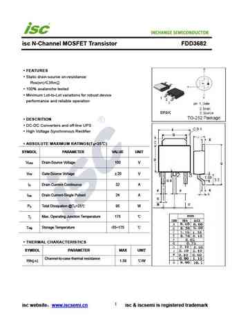
INCHANGE Semiconductor isc N-Channel MOSFET Transistor FDD3682 FEATURES Static drain-source on-resistance RDS(on) 36m 100% avalanche tested Minimum Lot-to-Lot variations for robust device performance and reliable operation DESCRITION DC-DC Converters and off-line UPS High Voltage Synchronous Rectifier ABSOLUTE MAXIMUM RATINGS(T =25 ) a SYMBOL PARAMETER VALUE... See More ⇒
Detailed specifications: FDD2670
, STU09N25
, FDD26AN06A0F085
, FDD306P
, FDD3510H
, STU06L01
, FDD3670
, STU04N20
, SI2302
, STU03N20
, FDD3672F085
, STU03L07
, STU03L01
, FDD3680
, FDD3682F085
, STT812A
, FDD3690
.
Keywords - FDD3672 MOSFET specs
FDD3672 cross reference
FDD3672 equivalent finder
FDD3672 pdf lookup
FDD3672 substitution
FDD3672 replacement
Can't find your MOSFET?
Learn how to find a substitute transistor by analyzing voltage, current and package compatibility