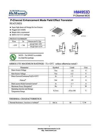
HM4953D Specs and Replacement
Type Designator: HM4953D
Type of Transistor: MOSFET
Type of Control Channel: P-Channel
Absolute Maximum Ratings
Pd ⓘ - Maximum Power Dissipation: 2 W
|Vds|ⓘ - Maximum Drain-Source Voltage: 20 V
|Vgs|ⓘ - Maximum Gate-Source Voltage: 12 V
|Id| ⓘ - Maximum Drain Current: 3 A
Tj ⓘ - Maximum Junction Temperature: 150 °C
Electrical Characteristics
tr ⓘ - Rise Time: 10 nS
Cossⓘ - Output Capacitance: 125 pF
Rds ⓘ - Maximum Drain-Source On-State Resistance: 0.075 Ohm
HM4953D substitution
- MOSFET ⓘ Cross-Reference Search
HM4953D datasheet
hm4953d.pdf
Shenzhen H&M Semiconductor Co.Ltd http //www.hmsemi.com Shenzhen H&M Semiconductor Co.Ltd http //www.hmsemi.com Shenzhen H&M Semiconductor Co.Ltd http //www.hmsemi.com Shenzhen H&M Semiconductor Co.Ltd http //www.hmsemi.com ... See More ⇒
chm4953jgp.pdf
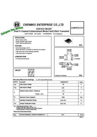
CHENMKO ENTERPRISE CO.,LTD CHM4953JGP SURFACE MOUNT Dual P-Channel Enhancement Mode Field Effect Transistor VOLTAGE 30 Volts CURRENT 4.9 Ampere APPLICATION * Servo motor control. * Power MOSFET gate drivers. * Other switching applications. SO-8 FEATURE * Small flat package. (SO-8 ) ( ) * Super high dense cell design for extremely low RDS(ON). 4.06 0.160 ( ) 3.70 0.146 * High ... See More ⇒
hm4953c.pdf
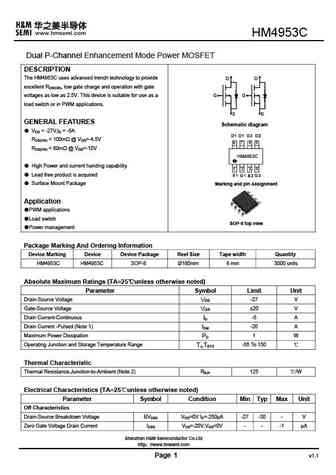
HM4953C Dual P-Channel Enhancement Mode Power MOSFET DESCRIPTION The HM4953C uses advanced trench technology to provide D D excellent RDS(ON), low gate charge and operation with gate voltages as low as 2.5V. This device is suitable for use as a G G load switch or in PWM applications. S S GENERAL FEATURES Schematic diagram VDS = -27V,ID = -5A RDS(ON) ... See More ⇒
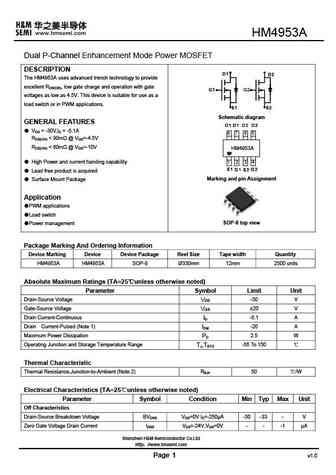
hm4953b.pdf

HM4953B Dual P-Channel Enhancement Mode Power MOSFET DESCRIPTION The HM4953B uses advanced trench technology to provide D D excellent RDS(ON), low gate charge and operation with gate voltages as low as 2.5V. This device is suitable for use as a G G load switch or in PWM applications. S S GENERAL FEATURES Schematic diagram VDS = -20V,ID = -5A RDS(ON) ... See More ⇒

Detailed specifications: HM4887 , HM4892A , HM4892B , HM4922 , HM4953 , HM4953A , HM4953B , HM4953C , IRFP460 , HM4963 , HM4N10PR , HM4N150T , HM4N60 , HM4N60F , HM4N60I , HM4N60K , HM4N65 .
Keywords - HM4953D MOSFET specs
HM4953D cross reference
HM4953D equivalent finder
HM4953D pdf lookup
HM4953D substitution
HM4953D replacement
Learn how to find the right MOSFET substitute. A guide to cross-reference, check specs and replace MOSFETs in your circuits.


LIST
Last Update
MOSFET: AOI780A70 | AOB42S60L | AOTF950A70L | AOTF27S60L | AOTF11S60L | AONV070V65G1 | AOM065V120X2Q | AOM033V120X2 | AOK500V120X2 | AOK065V65X2
Popular searches
2sc4793 | d965 | mje15031 | irfp150n | mj15025 | mp1620 | kta1381 | bf494