FDD6692 Specs and Replacement
Type Designator: FDD6692
Type of Transistor: MOSFET
Type of Control Channel: N-Channel
Absolute Maximum Ratings
Pd ⓘ - Maximum Power Dissipation: 57 W
|Vds|ⓘ - Maximum Drain-Source Voltage: 30 V
|Vgs|ⓘ - Maximum Gate-Source Voltage: 16 V
|Id| ⓘ - Maximum Drain Current: 54 A
Tj ⓘ - Maximum Junction Temperature: 175 °C
Electrical Characteristics
tr ⓘ - Rise Time: 5 nS
Cossⓘ - Output Capacitance: 357 pF
RDSonⓘ - Maximum Drain-Source On-State Resistance: 0.012 Ohm
Package: TO252
FDD6692 substitution
- MOSFET ⓘ Cross-Reference Search
FDD6692 datasheet
fdd6692 fdu6692.pdf
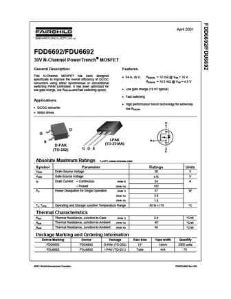
April 2001 FDD6692/FDU6692 30V N-Channel PowerTrench MOSFET General Description Features This N-Channel MOSFET has been designed 54 A, 30 V. RDS(ON) = 12 m @ VGS = 10 V specifically to improve the overall efficiency of DC/DC RDS(ON) = 14.5 m @ VGS = 4.5 V converters using either synchronous or conventional switching PWM controllers. It has been optim... See More ⇒
fdd6692.pdf

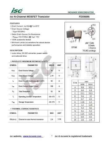
isc N-Channel MOSFET Transistor FDD6692 FEATURES Drain Current I =54A@ T =25 D C Drain Source Voltage V =30V(Min) DSS Static Drain-Source On-Resistance R =12m (Max) @ V = 10V DS(on) GS 100% avalanche tested Minimum Lot-to-Lot variations for robust device performance and reliable operation DESCRIPTION motor drive, DC-DC converter, power switch and solenoid dr... See More ⇒
fdd6690a.pdf
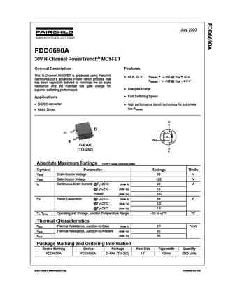
July 2003 FDD6690A 30V N-Channel PowerTrench MOSFET General Description Features This N-Channel MOSFET is produced using Fairchild 46 A, 30 V RDS(ON) = 12 m @ VGS = 10 V Semiconductor s advanced PowerTrench process that RDS(ON) = 14 m @ VGS = 4.5 V has been especially tailored to minimize the on state resistance and yet maintain low gate charge for Low gate charge su... See More ⇒
fdd6696.pdf
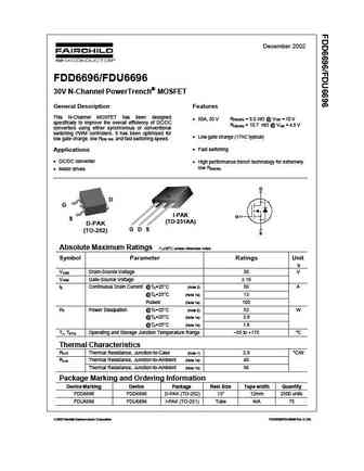
December 2002 FDD6696/FDU6696 30V N-Channel PowerTrench MOSFET General Description Features This N-Channel MOSFET has been designed 50A, 30 V R = 8.0 m @ V = 10 V DS(ON) GS specifically to improve the overall efficiency of DC/DC R = 10.7 m @ V = 4.5 V DS(ON) GS converters using either synchronous or conventional switching PWM controllers. It has been optimized for Low... See More ⇒

Detailed specifications: FDD6030BL, FDD603AL, FDD6644, FDU6644, FDD6670S, FDD6676, FDD6676S, FDD6680S, AOD4184A, FDU6692, FDH20N40, FDP20N40, FDH34N40, FMV60N280S2HF, IRF3305B, ISW65R041CFD, MDI5N40RH
Keywords - FDD6692 MOSFET specs
FDD6692 cross reference
FDD6692 equivalent finder
FDD6692 pdf lookup
FDD6692 substitution
FDD6692 replacement
Can't find your MOSFET? Learn how to find a substitute transistor by analyzing voltage, current and package compatibility
🌐 : EN ES РУ

LIST
Last Update
MOSFET: AUB034N10 | AUB033N08BG | AUB026N085 | AUA062N08BG | AUA060N08AG | AUA056N08BGL | AUA039N10 | ASW80R290E | ASW65R120EFD | ASW65R110E
Popular searches
irf4115 | 2sc828 replacement | 2sd669 datasheet | c102 transistor | bt152 datasheet | 2sa1302 datasheet | mpsa13 transistor equivalent | кт817г характеристики