NCE60P05R Specs and Replacement
Type Designator: NCE60P05R
Type of Transistor: MOSFET
Type of Control Channel: P-Channel
Absolute Maximum Ratings
Pd ⓘ
- Maximum Power Dissipation: 3.1 W
|Vds|ⓘ - Maximum Drain-Source Voltage: 60 V
|Vgs|ⓘ - Maximum Gate-Source Voltage: 20 V
|Id| ⓘ - Maximum Drain Current: 5 A
Tj ⓘ - Maximum Junction Temperature: 150 °C
Electrical Characteristics
tr ⓘ - Rise Time: 5 nS
Cossⓘ -
Output Capacitance: 93.7 pF
RDSonⓘ - Maximum Drain-Source On-State Resistance: 0.085 Ohm
Package: SOT-223
- MOSFET ⓘ Cross-Reference Search
NCE60P05R datasheet
..1. Size:492K ncepower
nce60p05r.pdf 
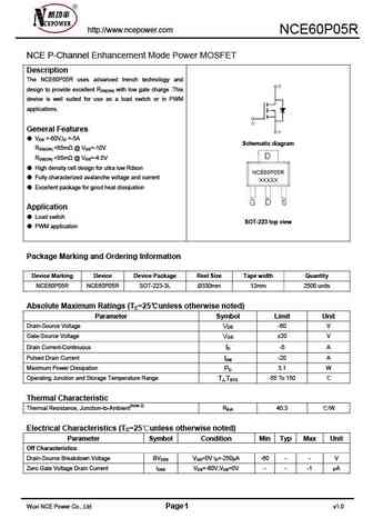
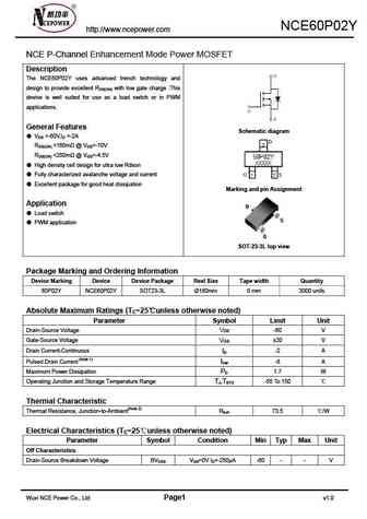
http //www.ncepower.com NCE60P05R NCE P-Channel Enhancement Mode Power MOSFET Description The NCE60P05R uses advanced trench technology and design to provide excellent RDS(ON) with low gate charge .This device is well suited for use as a load switch or in PWM applications. General Features VDS =-60V,ID =-5A Schematic diagram RDS(ON) ... See More ⇒
6.1. Size:411K ncepower
nce60p05n.pdf
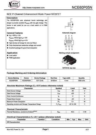
http //www.ncepower.com NCE60P05N NCE P-Channel Enhancement Mode Power MOSFET Description The NCE60P05N uses advanced trench technology and design to provide excellent RDS(ON) with low gate charge .This device is well suited for use as a load switch or in PWM applications. Schematic diagram General Features VDS =-60V,ID =-5A RDS(ON) ... See More ⇒
7.2. Size:364K ncepower
nce60p06s.pdf
http //www.ncepower.com NCE60P06S NCE P-Channel Enhancement Mode Power MOSFET Description The NCE60P06S uses advanced trench technology and design to provide excellent RDS(ON) with low gate charge. It can be used in a wide variety of applications. General Features VDS =-60V,ID =-6A RDS(ON) ... See More ⇒
7.3. Size:285K ncepower
nce60p09s.pdf
NCE60P09S http //www.ncepower.com NCE P-Channel Enhancement Mode Power MOSFET Description The NCE60P09S uses advanced trench technology and design to provide excellent RDS(ON) with low gate charge. It can be used in a wide variety of applications. General Features VDS =-60V,ID =-9A RDS(ON) ... See More ⇒
7.5. Size:656K ncepower
nce60p03r.pdf
http //www.ncepower.com NCE60P03R NCE P-Channel Enhancement Mode Power MOSFET Description General Features The NCE60P03R uses advanced trench technology and design V =-60V,I =-3A DS D to provide excellent R with low gate charge .This device is DS(ON) R ... See More ⇒
7.6. Size:358K ncepower
nce60p04sn.pdf
NCE60P04SN http //www.ncepower.com NCE P-Channel Enhancement Mode Power MOSFET Description The NCE60P04SN uses advanced trench technology and design to provide excellent RDS(ON) with low gate charge .This device is well suited for use as a load switch or in PWM applications. Schematic diagram General Features VDS =-60V,ID =-4A RDS(ON) ... See More ⇒
7.7. Size:288K ncepower
nce60p09as.pdf
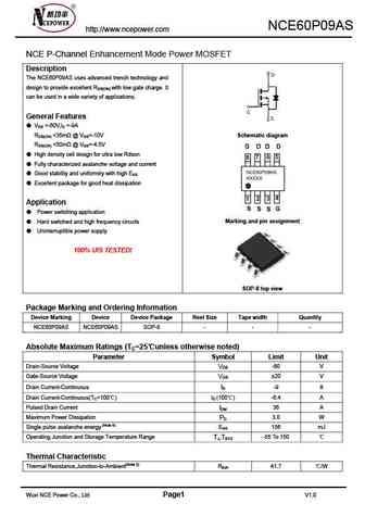
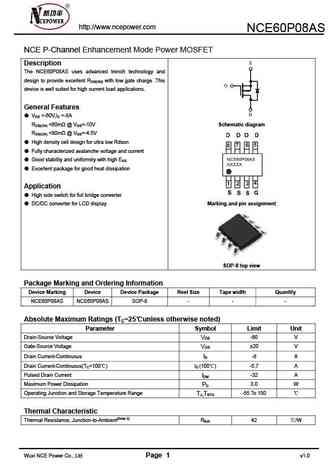
NCE60P09AS http //www.ncepower.com NCE P-Channel Enhancement Mode Power MOSFET Description The NCE60P09AS uses advanced trench technology and design to provide excellent RDS(ON) with low gate charge. It can be used in a wide variety of applications. General Features VDS =-60V,ID =-9A RDS(ON) ... See More ⇒
7.8. Size:371K ncepower
nce60p07as.pdf
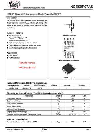
NCE60P07AS http //www.ncepower.com NCE P-Channel Enhancement Mode Power MOSFET Description The NCE60P07AS uses advanced trench technology and design to provide excellent RDS(ON) with low gate charge .This device is well suited for use as a load switch or in PWM applications. General Features VDS =-60V,ID =-7A Schematic diagram RDS(ON) ... See More ⇒
7.9. Size:655K ncepower
nce60p09k.pdf
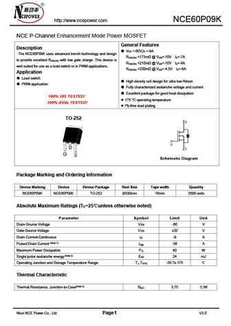
http //www.ncepower.com NCE60P09K NCE P-Channel Enhancement Mode Power MOSFET General Features Description V =-60V,I =-9A DS D The NCE60P09K uses advanced trench technology and design R ... See More ⇒
7.10. Size:344K ncepower
nce60p04y.pdf
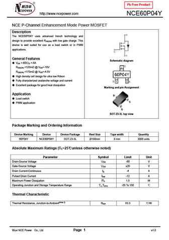
Pb Free Product http //www.ncepower.com NCE60P04Y NCE P-Channel Enhancement Mode Power MOSFET Description The NCE60P04Y uses advanced trench technology and design to provide excellent RDS(ON) with low gate charge .This device is well suited for use as a load switch or in PWM applications. General Features Schematic diagram VDS =-60V,ID =-4A RDS(ON) ... See More ⇒
7.11. Size:353K ncepower
nce60p03y.pdf
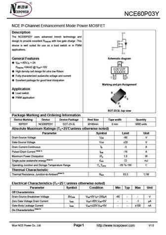
NCE60P03Y NCE P-Channel Enhancement Mode Power MOSFET Description The NCE60P03Y uses advanced trench technology and design to provide excellent RDS(ON) with low gate charge .This device is well suited for use as a load switch or in PWM applications. Schematic diagram General Features VDS =-60V,ID =-3A RDS(ON) ... See More ⇒
7.12. Size:333K ncepower
nce60p04r.pdf
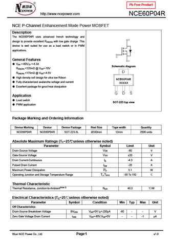
Pb Free Product http //www.ncepower.com NCE60P04R NCE P-Channel Enhancement Mode Power MOSFET Description The NCE60P04R uses advanced trench technology and design to provide excellent RDS(ON) with low gate charge .This device is well suited for use as a load switch or in PWM applications. General Features VDS =-60V,ID =-4.3A Schematic diagram RDS(ON) ... See More ⇒
Detailed specifications: NCE60NP2016G, NCE60NP4035K, NCE60P02Y, NCE60P03R, NCE60P03Y, NCE60P04SN, NCE60P05BY, NCE60P05N, AO3407, NCE60P07AS, NCE60P08AS, NCE60P09AS, NCE60P09K, NCE60P12AS, NCE60P16AQ, NCE60P17AQ, NCE60P18AQ
Keywords - NCE60P05R MOSFET specs
NCE60P05R cross reference
NCE60P05R equivalent finder
NCE60P05R pdf lookup
NCE60P05R substitution
NCE60P05R replacement
Step-by-step guide to finding a MOSFET replacement. Cross-reference parts and ensure compatibility for your repair or project.