NCEP023N85M Datasheet. Specs and Replacement
Type Designator: NCEP023N85M
Type of Transistor: MOSFET
Type of Control Channel: N-Channel
Absolute Maximum Ratings
Pd ⓘ - Maximum Power Dissipation: 300 W
|Vds|ⓘ - Maximum Drain-Source Voltage: 85 V
|Vgs|ⓘ - Maximum Gate-Source Voltage: 20 V
|Id| ⓘ - Maximum Drain Current: 260 A
Tj ⓘ - Maximum Junction Temperature: 175 °C
Electrical Characteristics
tr ⓘ - Rise Time: 37 nS
Cossⓘ - Output Capacitance: 2100 pF
RDSonⓘ - Maximum Drain-Source On-State Resistance: 0.0023 Ohm
Package: TO-220
NCEP023N85M substitution
- MOSFET ⓘ Cross-Reference Search
NCEP023N85M datasheet
ncep023n85m.pdf
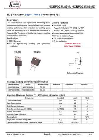
NCEP023N85M, NCEP023N85MD NCE N-Channel Super Trench II Power MOSFET Description The series of devices uses Super Trench II technology that is General Features uniquely optimized to provide the most efficient high frequency V =85V,I =260A DS D switching performance. Both conduction and switching power R =2.0m , typical (TO-220)@ V =10V DS(ON) GS losses are minimized due to an ex... See More ⇒
ncep023n85.pdf

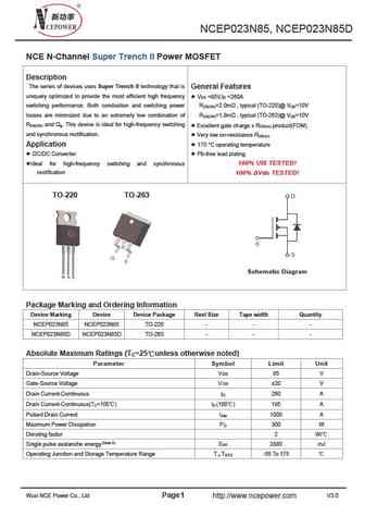
NCEP023N85, NCEP023N85D NCE N-Channel Super Trench II Power MOSFET Description The series of devices uses Super Trench II technology that is General Features uniquely optimized to provide the most efficient high frequency V =85V,I =260A DS D switching performance. Both conduction and switching power R =2.0m , typical (TO-220)@ V =10V DS(ON) GS losses are minimized due to an extr... See More ⇒
ncep023n85d.pdf
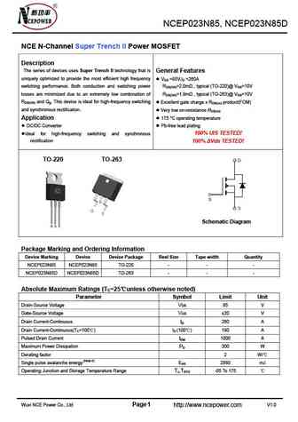
NCEP023N85, NCEP023N85D NCE N-Channel Super Trench II Power MOSFET Description The series of devices uses Super Trench II technology that is General Features uniquely optimized to provide the most efficient high frequency V =85V,I =260A DS D switching performance. Both conduction and switching power R =2.0m , typical (TO-220)@ V =10V DS(ON) GS losses are minimized due to an extr... See More ⇒
ncep023n85 ncep023n85d.pdf
NCEP023N85, NCEP023N85D NCE N-Channel Super Trench II Power MOSFET Description The series of devices uses Super Trench II technology that is General Features uniquely optimized to provide the most efficient high frequency VDS =85V,ID =260A switching performance. Both conduction and switching power RDS(ON)=2.0m , typical (TO-220)@ VGS=10V losses are minimized due to an ext... See More ⇒
Detailed specifications: NCEP0218G, NCEP0218K, NCEP0220F, NCEP0225F, NCEP0225G, NCEP0225K, NCEP0230D, NCEP023N10T, IRFP064N, NCEP023N85T, NCEP023NH30GU, NCEP02503S, NCEP02505S, NCEP02515F, NCEP02525G, NCEP02525K, NCEP02580D
Keywords - NCEP023N85M MOSFET specs
NCEP023N85M cross reference
NCEP023N85M equivalent finder
NCEP023N85M pdf lookup
NCEP023N85M substitution
NCEP023N85M replacement
Need a MOSFET replacement? Our guide shows you how to find a perfect substitute by comparing key parameters and specs
History: NCEP023N85T
🌐 : EN ES РУ

LIST
Last Update
MOSFET: FTF30P35D | FTF25N35DHVT | FTF15N35D | FTE15C35G | FTP02P15G | FTE02P15G | AKF30N5P0SX | AKF30N10S | AKF20P45D | CM4407
Popular searches
2sa1283 | 2sb646 | 2sc1885 datasheet | 2sc2580 | 2sc710 | 2sc968 | 2sd217 | bdw93c equivalent