NCEP2390 Datasheet. Specs and Replacement
Type Designator: NCEP2390
Type of Transistor: MOSFET
Type of Control Channel: N-Channel
Absolute Maximum Ratings
Pd ⓘ - Maximum Power Dissipation: 300 W
|Vds|ⓘ - Maximum Drain-Source Voltage: 230 V
|Vgs|ⓘ - Maximum Gate-Source Voltage: 20 V
|Id| ⓘ - Maximum Drain Current: 90 A
Tj ⓘ - Maximum Junction Temperature: 175 °C
Electrical Characteristics
tr ⓘ - Rise Time: 26 nS
Cossⓘ - Output Capacitance: 333.1 pF
RDSonⓘ - Maximum Drain-Source On-State Resistance: 0.0155 Ohm
Package: TO-220
NCEP2390 substitution
- MOSFET ⓘ Cross-Reference Search
NCEP2390 datasheet
ncep2390.pdf
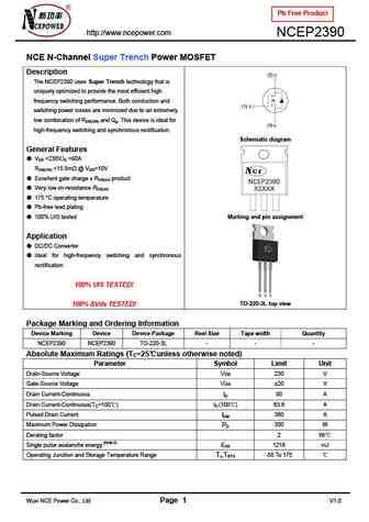
Pb Free Product http //www.ncepower.com NCEP2390 NCE N-Channel Super Trench Power MOSFET Description The NCEP2390 uses Super Trench technology that is uniquely optimized to provide the most efficient high frequency switching performance. Both conduction and switching power losses are minimized due to an extremely low combination of RDS(ON) and Qg. This device is ideal for high... See More ⇒
ncep2390d.pdf
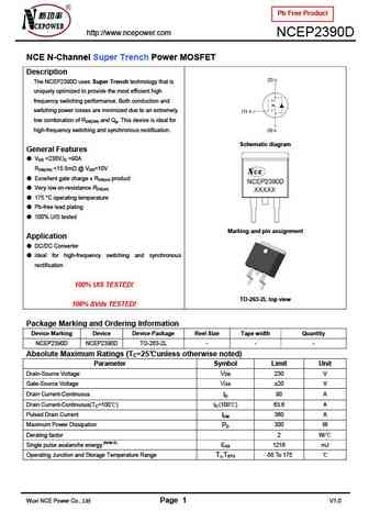
Pb Free Product http //www.ncepower.com NCEP2390D NCE N-Channel Super Trench Power MOSFET Description The NCEP2390D uses Super Trench technology that is uniquely optimized to provide the most efficient high frequency switching performance. Both conduction and switching power losses are minimized due to an extremely low combination of RDS(ON) and Qg. This device is ideal for hi... See More ⇒
ncep25nd10ag.pdf
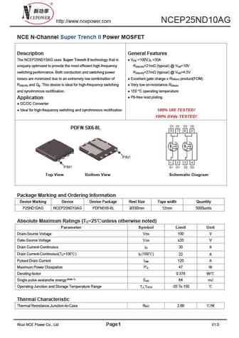
http //www.ncepower.com NCEP25ND10AG NCE N-Channel Super Trench II Power MOSFET Description General Features The NCEP25ND10AG uses Super Trench II technology that is V =100V,I =30A DS D uniquely optimized to provide the most efficient high frequency R =21m (typical) @ V =10V DS(ON) GS switching performance. Both conduction and switching power R =27m (typical) @ V =4.5V DS(ON) GS... See More ⇒
ncep25n10ad.pdf
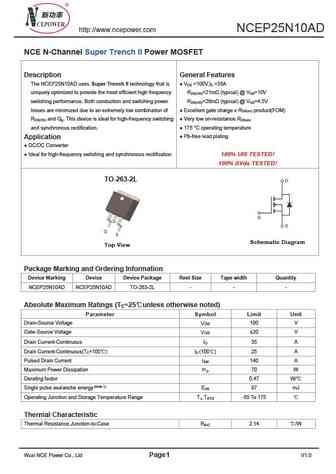
http //www.ncepower.com NCEP25N10AD NCE N-Channel Super Trench II Power MOSFET Description General Features The NCEP25N10AD uses Super Trench II technology that is V =100V,I =35A DS D uniquely optimized to provide the most efficient high frequency R =21m (typical) @ V =10V DS(ON) GS switching performance. Both conduction and switching power R =26m (typical) @ V =4.5V DS(ON) GS ... See More ⇒
Detailed specifications: NCEP15T14T, NCEP15T18T, NCEP15T26LL, NCEP16N85AK, NCEP18N10AG, NCEP18N10AK, NCEP18N10AQ, NCEP18N10AR, AO3400, NCEP2390D, NCEP25N10AD, NCEP25N10AG, NCEP25N10AQ, NCEP25ND10AG, NCEP3045BGU, NCEP3045GU, NCEP3060EQ
Keywords - NCEP2390 MOSFET specs
NCEP2390 cross reference
NCEP2390 equivalent finder
NCEP2390 pdf lookup
NCEP2390 substitution
NCEP2390 replacement
Learn how to find the right MOSFET substitute. A guide to cross-reference, check specs and replace MOSFETs in your circuits.
🌐 : EN ES РУ

LIST
Last Update
MOSFET: ASDM40N60KQ | ASDM40N40E | ASDM40N100P | ASDM40DN20E | ASDM3416EZA | ASDM3415ZA | ASDM3401ZA | ASDM3401 | ASDM3400ZA | ASDM30P30BE
Popular searches
mj2955 | mje15030 | 2n3904 transistor | 2sd424 | 2sc828 | 2n4125 | tip42c transistor | c1815 transistor datasheet