FIR110N10PG Specs and Replacement
Type Designator: FIR110N10PG
Type of Transistor: MOSFET
Type of Control Channel: N-Channel
Absolute Maximum Ratings
Pd ⓘ - Maximum Power Dissipation: 220 W
|Vds|ⓘ - Maximum Drain-Source Voltage: 100 V
|Vgs|ⓘ - Maximum Gate-Source Voltage: 20 V
|Id| ⓘ - Maximum Drain Current: 110 A
Tj ⓘ - Maximum Junction Temperature: 175 °C
Electrical Characteristics
tr ⓘ - Rise Time: 24 nS
Cossⓘ - Output Capacitance: 380 pF
RDSonⓘ - Maximum Drain-Source On-State Resistance: 0.009 Ohm
Package: TO-220AB
FIR110N10PG substitution
- MOSFET ⓘ Cross-Reference Search
FIR110N10PG datasheet
fir110n10pg.pdf
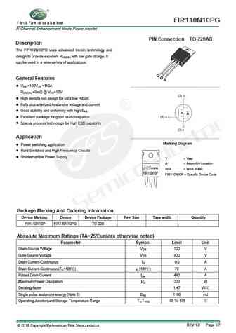
FIR110N10PG N-Channel Enhancement Mode Power Mosfet PIN Connection TO-220AB Description The FIR110N10PG uses advanced trench technology and design to provide excellent RDS(ON) with low gate charge. It can be used in a wide variety of applications. General Features VDS =100V,ID =110A RDS(ON) ... See More ⇒
fir11ns65afg.pdf
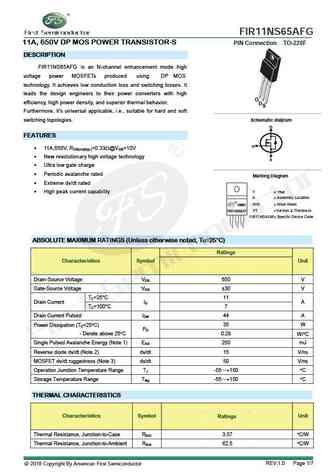
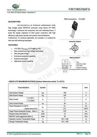
FIR11NS65AFG 11A, 650V DP MOS POWER TRANSISTOR-S PIN Connection TO-220F DESCRIPTION FIR11NS65AFG is an N-channel enhancement mode high voltage power MOSFETs produced using DP MOS technology. It achieves low conduction loss and switching losses. It leads the design engineers to their power converters with high G efficiency, high power density, and superior thermal behavior. D S ... See More ⇒
fir11n90ang.pdf
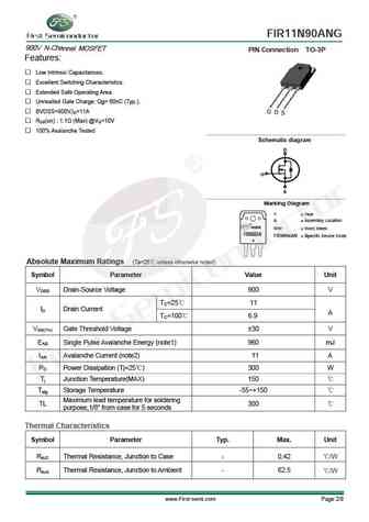
FIR11N90ANG 900V N-Channel MOSFET PIN Connection TO-3P Features Low Intrinsic Capacitances. Excellent Switching Characteristics. Extended Safe Operating Area. Unrivalled Gate Charge Qg= 60nC (Typ.). BVDSS=900V,ID=11A RDS(on) 1.1 (Max) @VG=10V 100% Avalanche Tested g Schematic dia ram D G S Marking Diagram Y = Year A = Assembly Location ... See More ⇒
fir11n40fg.pdf
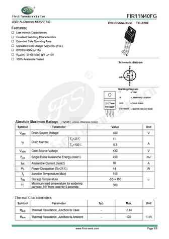
FIR11N40FG 400V N-Channel MOSFET-G PIN Connection TO-220F Features Low Intrinsic Capacitances. Excellent Switching Characteristics. Extended Safe Operating Area. Unrivalled Gate Charge Qg=27nC (Typ.). BVDSS=400V,ID=11A G DS RDS(on) 0.4 (Max) @V =10V G 100% Avalanche Tested g Schematic dia ram D G S Marking Diagram Y = Year A = Assembly Loc... See More ⇒
Detailed specifications: FDM80R120AN4G, FDZ65T300D8G, FDZ90T150PG, FIR10N10LG, FIR10N20LG, FIR10N50FG, FIR10N70FG, FIR10N80FG, 50N06, FIR11N40FG, FIR11N90ANG, FIR11NS65AFG, FIR11NS70AFG, FIR120N08PG, FIR12N15LG, FIR12N70FG, FIR12N80FG
Keywords - FIR110N10PG MOSFET specs
FIR110N10PG cross reference
FIR110N10PG equivalent finder
FIR110N10PG pdf lookup
FIR110N10PG substitution
FIR110N10PG replacement
Step-by-step guide to finding a MOSFET replacement. Cross-reference parts and ensure compatibility for your repair or project.
History: FTK4N70F
🌐 : EN ES РУ

LIST
Last Update
MOSFET: CM4407 | CM3407 | CM3400 | SVF11N65F | SVF11N65T | FKBB3105 | EHBA036R1 | CRTT067N10N | AP6NA3R2MT | AP65SA145DDT8
Popular searches
2sa818 replacement | irfb3607 datasheet | 2n2907 equivalent | c2026 | mpsa56 transistor equivalent | 13009 transistor | irf3205 equivalent | ksa992 transistor