P0610BT Datasheet. Specs and Replacement
Type Designator: P0610BT 📄📄
Type of Transistor: MOSFET
Type of Control Channel: N-Channel
Absolute Maximum Ratings
Pd ⓘ - Maximum Power Dissipation: 208 W
|Vds|ⓘ - Maximum Drain-Source Voltage: 100 V
|Vgs|ⓘ - Maximum Gate-Source Voltage: 20 V
|Id| ⓘ - Maximum Drain Current: 120 A
Tj ⓘ - Maximum Junction Temperature: 150 °C
Electrical Characteristics
tr ⓘ - Rise Time: 60 nS
Cossⓘ - Output Capacitance: 747 pF
RDSonⓘ - Maximum Drain-Source On-State Resistance: 0.0065 Ohm
Package: TO-220
P0610BT substitution
- MOSFET ⓘ Cross-Reference Search
P0610BT datasheet
p0610bt.pdf
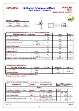
P0610BT N-Channel Enhancement Mode NIKO-SEM TO-220 Field Effect Transistor Halogen-Free & Lead-Free D PRODUCT SUMMARY V(BR)DSS RDS(ON) ID2 1. GATE G 100V 6.5m 120A 2. DRAIN 3. SOURCE S ABSOLUTE MAXIMUM RATINGS (TA = 25 C Unless Otherwise Noted) PARAMETERS/TEST CONDITIONS SYMBOL LIMITS UNITS Drain-Source Voltage VDS 100 V Gate-Source Voltage VGS 20 V TC = ... See More ⇒
p0610btf.pdf
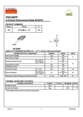
P0610BTF N-Channel Enhancement Mode MOSFET PRODUCT SUMMARY V(BR)DSS RDS(ON) ID 6.5m @VGS = 10V 100V 66A TO-220F ABSOLUTE MAXIMUM RATINGS (TA = 25 C Unless Otherwise Noted) PARAMETERS/TEST CONDITIONS SYMBOL LIMITS UNITS VDS Drain-Source Voltage 100 V VGS Gate-Source Voltage 20 TC = 25 C 66 ID Continuous Drain Current TC = 100 C 41 A IDM 200 Pulsed Drain Cur... See More ⇒
p0610btf.pdf
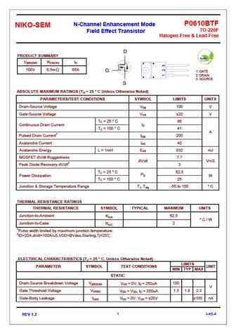
P0610BTF N-Channel Enhancement Mode NIKO-SEM TO-220F Field Effect Transistor Halogen-Free & Lead-Free D PRODUCT SUMMARY V(BR)DSS RDS(ON) ID 100V 6.5m 66A G 1 GATE 2 DRAIN 3 SOURCE S ABSOLUTE MAXIMUM RATINGS (TA = 25 C Unless Otherwise Noted) PARAMETERS/TEST CONDITIONS SYMBOL LIMITS UNITS Drain-Source Voltage VDS 100 V Gate-Source Voltage VGS 20 V TC... See More ⇒
tp0610k.pdf
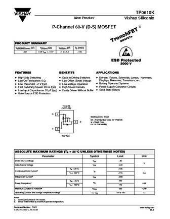
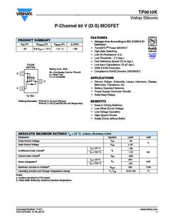
TP0610K New Product Vishay Siliconix P-Channel 60-V (D-S) MOSFET PRODUCT SUMMARY V(BR)DSS(min) (V) rDS(on) (W) VGS(th) (V) ID (mA) 60 6 @ VGS = 10 V 1 to 3.0 185 FEATURES BENEFITS APPLICATIONS D High-Side Switching D Ease in Driving Switches D Drivers Relays, Solenoids, Lamps, Hammers, Displays, Memories, Transistors, etc. D Low On-Resistance 6 D Low Offset (Error... See More ⇒

Detailed specifications: P0260EIA, P0306BT, P0406AK, P0460EDA, P0470ED, P0470ETF, P0470JD, P0508AT, SPP20N60C3, P0620ED, P0660ED, P0660EI, P0706BD, P0706BK, P0706BV, P0765JD, P0770ED
Keywords - P0610BT MOSFET specs
P0610BT cross reference
P0610BT equivalent finder
P0610BT pdf lookup
P0610BT substitution
P0610BT replacement
Learn how to find the right MOSFET substitute. A guide to cross-reference, check specs and replace MOSFETs in your circuits.
History: P0470ED | P0508AT
🌐 : EN ES РУ

LIST
Last Update
MOSFET: ASDM30P100KQ | ASDM30N90Q | ASDM30N75KQ | ASDM30N150Q | ASDM30N120Q | ASDM30N120KQ | ASDM30N100KQ | ASDM30DN40E | ASDM30DN30E | ASDM3050KQ
Popular searches
2n414 | c3998 | c4468 datasheet | 2sc2603 | jcs50n20wt | 2sa1360 | p60nf06 datasheet | 2sc4468