PX5D8JZ-T Datasheet. Specs and Replacement
Type Designator: PX5D8JZ-T 📄📄
Type of Transistor: MOSFET
Type of Control Channel: N-Channel
Absolute Maximum Ratings
Pd ⓘ - Maximum Power Dissipation: 0.31 W
|Vds|ⓘ - Maximum Drain-Source Voltage: 20 V
|Vgs|ⓘ - Maximum Gate-Source Voltage: 10 V
|Id| ⓘ - Maximum Drain Current: 0.78 A
Tj ⓘ - Maximum Junction Temperature: 150 °C
Electrical Characteristics
tr ⓘ - Rise Time: 36 nS
Cossⓘ - Output Capacitance: 19 pF
RDSonⓘ - Maximum Drain-Source On-State Resistance: 0.3 Ohm
Package: SOT-563
📄📄 Copy
PX5D8JZ-T substitution
- MOSFET ⓘ Cross-Reference Search
PX5D8JZ-T datasheet
px5d8jz-t.pdf

Dual N-Channel Logic Level PX5D8JZ-T NIKO-SEM Enhancement Mode Field Effect Transistor SOT-563 Halogen-Free & Lead-Free PRODUCT SUMMARY 1 2 V(BR)DSS RDS(ON) ID 20V 300m 0.78A 1 2 1 2 Features Pb-Free, Halogen Free and RoHS compliant. Low RDS(on) to Minimize Conduction Losses. Ohmic Region Good RDS(on) Ratio. Optimized Gate Charge to Minimize... See More ⇒
px5d8ea.pdf
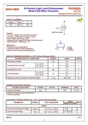
N-Channel Logic Level Enhancement PX5D8EA NIKO-SEM Mode Field Effect Transistor SOT-523 Halogen-Free & Lead-Free PRODUCT SUMMARY V(BR)DSS RDS(ON) ID 20V 300m 0.8A Features Pb-Free, Halogen Free and RoHS compliant. Low RDS(on) to Minimize Conduction Losses. Ohmic Region Good RDS(on) Ratio. Optimized Gate Charge to Minimize Switching Losses. ESD ... See More ⇒
Detailed specifications: PV6A8BA, PV6D2DA, PW567EA, PW5D8EA, PW5S6EA, PX567EA, PX567JZ, PX5D8EA, IRLB4132, PX5S6EA, PX5S6JZ, PX607UZ, PZ5203EMAA, PZ567JZ, PZ5D8EA, PZ5D8JZ, PZ5G7EA
Keywords - PX5D8JZ-T MOSFET specs
PX5D8JZ-T cross reference
PX5D8JZ-T equivalent finder
PX5D8JZ-T pdf lookup
PX5D8JZ-T substitution
PX5D8JZ-T replacement
Need a MOSFET replacement? Our guide shows you how to find a perfect substitute by comparing key parameters and specs
MOSFET Parameters. How They Affect Each Other
History: HM6400 | AGM15T06H | DHBSJ11N65 | DHF10H037R | IXFH50N30Q3 | HM6N10R | JMH65R190APLNFD
🌐 : EN ES РУ

LIST
Last Update
MOSFET: CS95118 | CS85105A | CS75N45 | CS72N12 | CS55N50 | CS48N75A | CS40N27 | MSQ60P04D | MSQ40P07D | MSQ30P40D
Popular searches
a1016 transistor | a1693 transistor | a933 datasheet | c535 transistor | irf3205 reemplazo | mpsu06 | кт630 | 2g381 transistor