CED3133 Datasheet. Specs and Replacement
Type Designator: CED3133 📄📄
Type of Transistor: MOSFET
Type of Control Channel: P-Channel
Absolute Maximum Ratings
Pd ⓘ - Maximum Power Dissipation: 31 W
|Vds|ⓘ - Maximum Drain-Source Voltage: 30 V
|Vgs|ⓘ - Maximum Gate-Source Voltage: 25 V
|Id| ⓘ - Maximum Drain Current: 35 A
Tj ⓘ - Maximum Junction Temperature: 150 °C
Electrical Characteristics
tr ⓘ - Rise Time: 8 nS
Cossⓘ - Output Capacitance: 260 pF
RDSonⓘ - Maximum Drain-Source On-State Resistance: 0.016 Ohm
Package: TO251
📄📄 Copy
CED3133 substitution
- MOSFET ⓘ Cross-Reference Search
CED3133 datasheet
ced3133 ceu3133.pdf
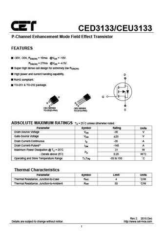
CED3133/CEU3133 P-Channel Enhancement Mode Field Effect Transistor FEATURES -30V, -35A, RDS(ON) = 16mW @VGS = -10V. RDS(ON) = 27mW @VGS = -4.5V. Super high dense cell design for extremely low RDS(ON). High power and current handing capability. D RoHS compliant. TO-251 & TO-252 package. D G G S CEU SERIES CED SERIES S TO-252(D-PAK) TO-251(I-PAK) ABSOLUTE MAXIMUM RATINGS Tc = 2... See More ⇒
ced3120 ceu3120.pdf

CED3120/CEU3120 N-Channel Enhancement Mode Field Effect Transistor FEATURES 30V, 36A , RDS(ON) = 15m @VGS = 10V. RDS(ON) = 22m @VGS = 4.5V. Super high dense cell design for extremely low RDS(ON). High power and current handing capability. D Lead free product is acquired. TO-251 & TO-252 package. D G G S CEU SERIES CED SERIES S TO-252(D-PAK) TO-251(I-PAK) ABSOLUTE MAXIMU... See More ⇒
ceu3172 ced3172.pdf
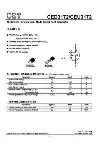
CED3172/CEU3172 N-Channel Enhancement Mode Field Effect Transistor FEATURES 30V, 36A, RDS(ON) = 20m @VGS = 10V. RDS(ON) = 32m @VGS = 4.5V. Super high dense cell design for extremely low RDS(ON). D High power and current handing capability. Lead free product is acquired. TO-251 & TO-252 package. D G G S CEU SERIES CED SERIES S TO-252(D-PAK) TO-251(I-PAK) ABSOLUTE MAXIMUM... See More ⇒
ceu3120 ced3120.pdf
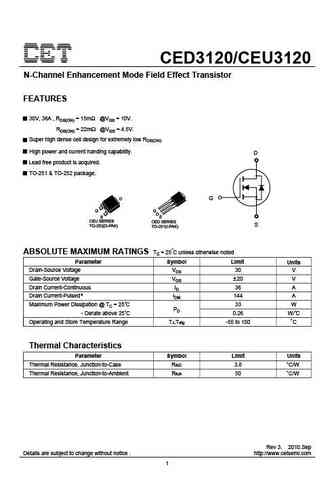
CED3120/CEU3120 N-Channel Enhancement Mode Field Effect Transistor FEATURES 30V, 36A , RDS(ON) = 15m @VGS = 10V. RDS(ON) = 22m @VGS = 4.5V. Super high dense cell design for extremely low RDS(ON). High power and current handing capability. D Lead free product is acquired. TO-251 & TO-252 package. D G G S CEU SERIES CED SERIES S TO-252(D-PAK) TO-251(I-PAK) ABSOLUTE MAXIMU... See More ⇒
Detailed specifications: BC2302-2.8A, BC2302T-2.8A, BC2302W, BC3134K, BC3134KT, CEB100N10L, CEC2533, CEC3257, IRF1405
Keywords - CED3133 MOSFET specs
CED3133 cross reference
CED3133 equivalent finder
CED3133 pdf lookup
CED3133 substitution
CED3133 replacement
Need a MOSFET replacement? Our guide shows you how to find a perfect substitute by comparing key parameters and specs
MOSFET Parameters. How They Affect Each Other
History: CEM3115
🌐 : EN ES РУ

LIST
Last Update
MOSFET: CEM3139 | CEM3133 | CEM3115 | CED3133 | CEC3257 | CEC2533 | CEB100N10L | BC3134KT | BC3134K | BC2302W
Popular searches
s9018 | 2n3904 equivalent | ksa1220 | s9015 | mje3055t datasheet | a733 | irf9630 | mj2955