CEM3139 Datasheet. Specs and Replacement
Type Designator: CEM3139 📄📄
Type of Transistor: MOSFET
Type of Control Channel: NP-Channel
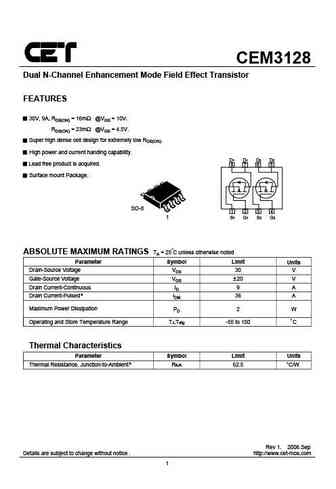
Absolute Maximum Ratings
Pd ⓘ - Maximum Power Dissipation: 2 W
|Vds|ⓘ - Maximum Drain-Source Voltage: 30 V
|Vgs|ⓘ - Maximum Gate-Source Voltage: 12 V
|Id| ⓘ - Maximum Drain Current: 9_6 A
Tj ⓘ - Maximum Junction Temperature: 150 °C
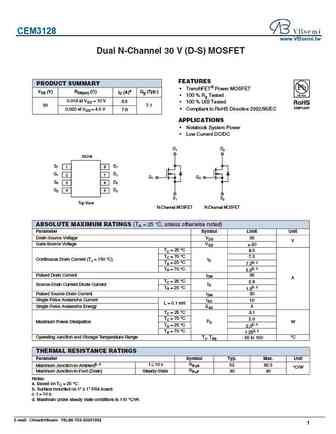
Electrical Characteristics
tr ⓘ - Rise Time: 10_5 nS
Cossⓘ - Output Capacitance: 205_210 pF
RDSonⓘ - Maximum Drain-Source On-State Resistance: 0.016_0.034 Ohm
Package: SO8
📄📄 Copy
CEM3139 substitution
- MOSFET ⓘ Cross-Reference Search
CEM3139 datasheet
cem3139.pdf
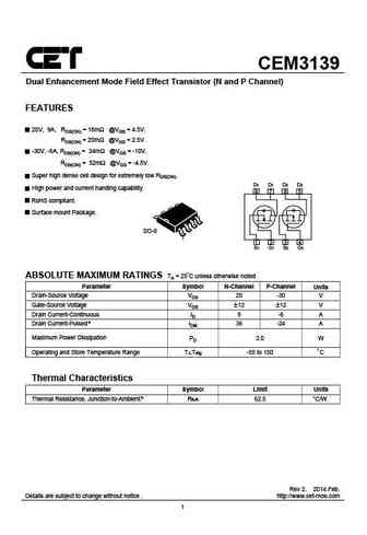
CEM3139 Dual Enhancement Mode Field Effect Transistor (N and P Channel) FEATURES 20V, 9A, RDS(ON) = 16m @VGS = 4.5V. RDS(ON) = 20m @VGS = 2.5V. -30V, -6A, RDS(ON) = 34m @VGS = -10V. RDS(ON) = 52m @VGS = -4.5V. Super high dense cell design for extremely low RDS(ON). D1 D1 D2 D2 High power and current handing capability. 8 7 6 5 RoHS compliant. Surface mount Package. S... See More ⇒
cem3138.pdf
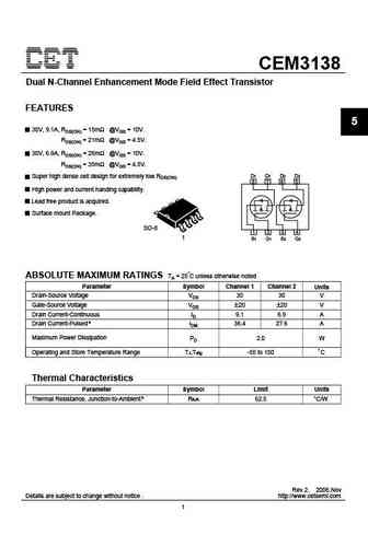
CEM3138 Dual N-Channel Enhancement Mode Field Effect Transistor FEATURES 5 30V, 9.1A, RDS(ON) = 15m @VGS = 10V. RDS(ON) = 21m @VGS = 4.5V. 30V, 6.9A, RDS(ON) = 26m @VGS = 10V. RDS(ON) = 35m @VGS = 4.5V. D1 D1 D2 D2 Super high dense cell design for extremely low RDS(ON). 8 7 6 5 High power and current handing capability. Lead free product is acquired. Surface mount Pac... See More ⇒
cem3133.pdf
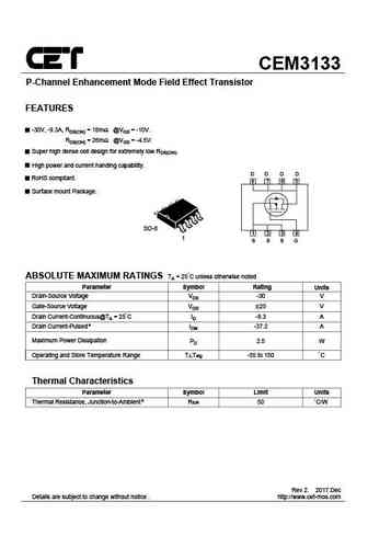
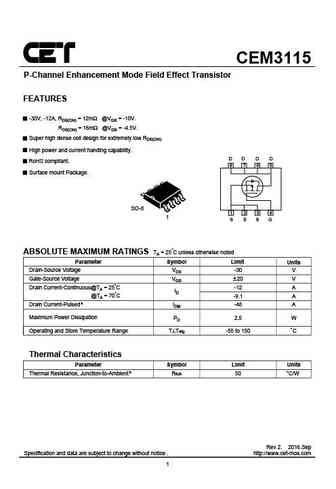
CEM3133 P-Channel Enhancement Mode Field Effect Transistor FEATURES -30V, -9.3A, RDS(ON) = 18mW @VGS = -10V. RDS(ON) = 26mW @VGS = -4.5V. Super high dense cell design for extremely low RDS(ON). High power and current handing capability. D D D D RoHS compliant. 8 7 6 5 Surface mount Package. SO-8 1 2 3 4 1 S S S G ABSOLUTE MAXIMUM RATINGS TA = 25 C unless otherwise noted Parame... See More ⇒
cem3109.pdf
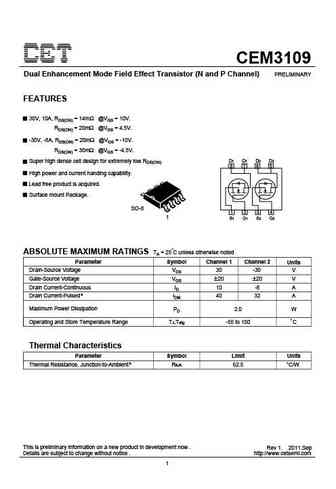
CEM3109 Dual Enhancement Mode Field Effect Transistor (N and P Channel) PRELIMINARY FEATURES 30V, 10A, RDS(ON) = 14m @VGS = 10V. RDS(ON) = 20m @VGS = 4.5V. -30V, -8A, RDS(ON) = 20m @VGS = -10V. RDS(ON) = 30m @VGS = -4.5V. D1 D1 D2 D2 Super high dense cell design for extremely low RDS(ON). 8 7 6 5 High power and current handing capability. Lead free product is acquired. ... See More ⇒
Detailed specifications: BC3134K, BC3134KT, CEB100N10L, CEC2533, CEC3257, CED3133, CEM3115, CEM3133, HY1906P
Keywords - CEM3139 MOSFET specs
CEM3139 cross reference
CEM3139 equivalent finder
CEM3139 pdf lookup
CEM3139 substitution
CEM3139 replacement
Learn how to find the right MOSFET substitute. A guide to cross-reference, check specs and replace MOSFETs in your circuits.
MOSFET Parameters. How They Affect Each Other
History: CEM3115
🌐 : EN ES РУ

LIST
Last Update
MOSFET: CEM3139 | CEM3133 | CEM3115 | CED3133 | CEC3257 | CEC2533 | CEB100N10L | BC3134KT | BC3134K | BC2302W
Popular searches
s9015 | mje3055t datasheet | a733 | irf9630 | mj2955 | mje15030 | 2n3904 transistor | 2sd424