MTD6N20E Datasheet. Specs and Replacement
Type Designator: MTD6N20E 📄📄
Type of Transistor: MOSFET
Type of Control Channel: N-Channel
Absolute Maximum Ratings
Pd ⓘ - Maximum Power Dissipation: 50 W
|Vds|ⓘ - Maximum Drain-Source Voltage: 200 V
|Vgs|ⓘ - Maximum Gate-Source Voltage: 20 V
|Id| ⓘ - Maximum Drain Current: 6 A
Tj ⓘ - Maximum Junction Temperature: 150 °C
Electrical Characteristics
tr ⓘ - Rise Time: 29 nS
Cossⓘ - Output Capacitance: 92 pF
RDSonⓘ - Maximum Drain-Source On-State Resistance: 0.7 Ohm
Package: DPAK
📄📄 Copy
MTD6N20E substitution
- MOSFET ⓘ Cross-Reference Search
MTD6N20E datasheet
mtd6n20e.pdf
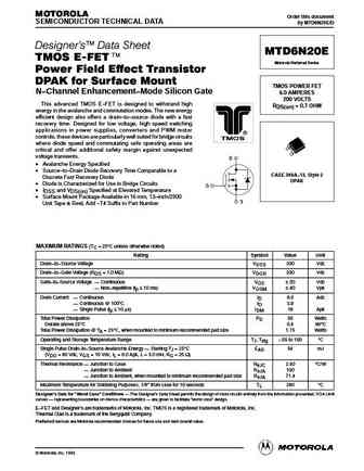
MOTOROLA Order this document SEMICONDUCTOR TECHNICAL DATA by MTD6N20E/D Designer's Data Sheet MTD6N20E TMOS E-FET. Motorola Preferred Device Power Field Effect Transistor DPAK for Surface Mount TMOS POWER FET N Channel Enhancement Mode Silicon Gate 6.0 AMPERES 200 VOLTS This advanced TMOS E FET is designed to withstand high RDS(on) = 0.7 OHM energy in the avalanche an... See More ⇒
mtd6n20e-d.pdf
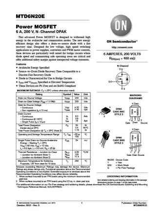
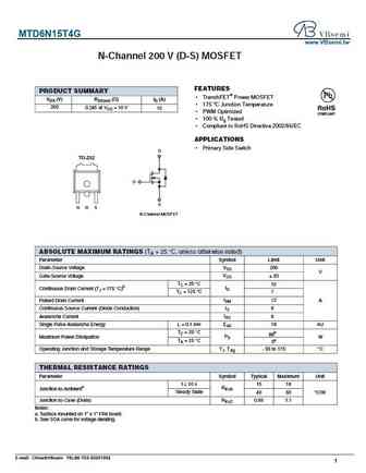
MTD6N20E Power MOSFET 6 A, 200 V, N-Channel DPAK This advanced Power MOSFET is designed to withstand high energy in the avalanche and commutation modes. The new energy efficient design also offers a drain-to-source diode with a fast recovery time. Designed for low voltage, high speed switching http //onsemi.com applications in power supplies, converters and PWM motor controls, these de... See More ⇒
mtd6n20et4 mtd6n20et4g.pdf
MTD6N20E Power MOSFET 6 A, 200 V, N-Channel DPAK This advanced Power MOSFET is designed to withstand high energy in the avalanche and commutation modes. The new energy efficient design also offers a drain-to-source diode with a fast recovery time. Designed for low voltage, high speed switching http //onsemi.com applications in power supplies, converters and PWM motor controls, these de... See More ⇒
mtd6n15r.pdf
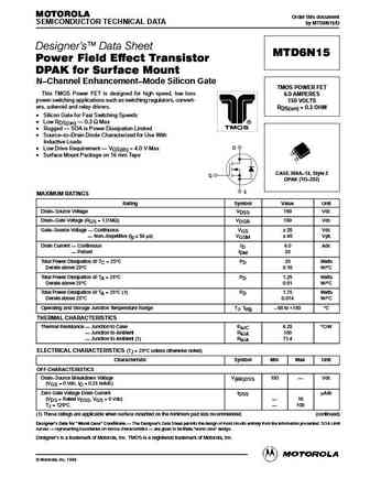
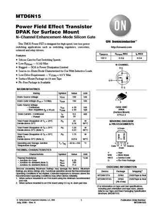
MOTOROLA Order this document SEMICONDUCTOR TECHNICAL DATA by MTD6N15/D Designer's Data Sheet MTD6N15 Power Field Effect Transistor DPAK for Surface Mount N Channel Enhancement Mode Silicon Gate TMOS POWER FET This TMOS Power FET is designed for high speed, low loss 6.0 AMPERES power switching applications such as switching regulators, convert- 150 VOLTS ers, solenoid and re... See More ⇒
Detailed specifications: MMDF1N05E, MMFT960, MMSF3P02HD, MPF4393, MTB2P50E, MTB50P03HDL, MTD5P06V, MTD6N15, AO3407, MTP20N15E, MTP2P50E, MTP50P03HDL, MTW32N20E, NCV8401, NCV8402, NCV8402D, NCV8403
Keywords - MTD6N20E MOSFET specs
MTD6N20E cross reference
MTD6N20E equivalent finder
MTD6N20E pdf lookup
MTD6N20E substitution
MTD6N20E replacement
Can't find your MOSFET? Learn how to find a substitute transistor by analyzing voltage, current and package compatibility
MOSFET Parameters. How They Affect Each Other
History: CSD19505KCS | 2N7297 | MTP4N50 | 2SK1712
🌐 : EN ES РУ
LIST
Last Update
MOSFET: CS95118 | CS85105A | CS75N45 | CS72N12 | CS55N50 | CS48N75A | CS40N27 | MSQ60P04D | MSQ40P07D | MSQ30P40D
Popular searches
2sa970 datasheet | 2sc1627 | aoe6936 datasheet | g40t60an3h datasheet | j5027-r datasheet | transistor a1015 datasheet | bf199 transistor equivalent | bu801
