NVTFS4823N Specs and Replacement
Type Designator: NVTFS4823N
Type of Transistor: MOSFET
Type of Control Channel: N-Channel
Absolute Maximum Ratings
Pd ⓘ - Maximum Power Dissipation: 3.1 W
|Vds|ⓘ - Maximum Drain-Source Voltage: 30 V
|Vgs|ⓘ - Maximum Gate-Source Voltage: 20 V
|Id| ⓘ - Maximum Drain Current: 13 A
Tj ⓘ - Maximum Junction Temperature: 175 °C
Electrical Characteristics
tr ⓘ - Rise Time: 22 nS
Cossⓘ - Output Capacitance: 175 pF
RDSonⓘ - Maximum Drain-Source On-State Resistance: 0.0105 Ohm
Package: WDFN8
NVTFS4823N substitution
- MOSFET ⓘ Cross-Reference Search
NVTFS4823N datasheet
nvtfs4823n-d.pdf
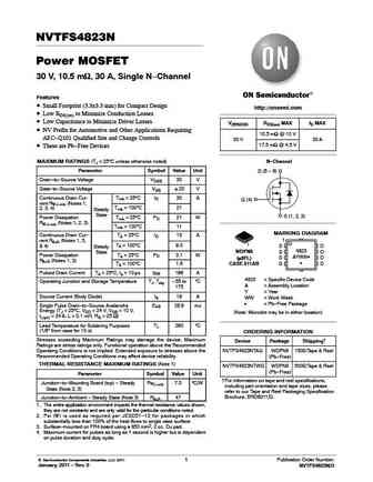
NVTFS4823N Power MOSFET 30 V, 10.5 mW, 30 A, Single N-Channel Features Small Footprint (3.3x3.3 mm) for Compact Design http //onsemi.com Low RDS(on) to Minimize Conduction Losses Low Capacitance to Minimize Driver Losses V(BR)DSS RDS(on) MAX ID MAX NV Prefix for Automotive and Other Applications Requiring 10.5 mW @ 10 V AEC-Q101 Qualified Site and Change Controls 30 ... See More ⇒
nvtfs4824n.pdf
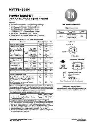
NVTFS4824N Power MOSFET 30 V, 4.7 mW, 46 A, Single N-Channel Features Small Footprint (3.3 x 3.3 mm) for Compact Design Low RDS(on) to Minimize Conduction Losses http //onsemi.com Low Capacitance to Minimize Driver Losses NVTFS4824NWF - Wettable Flanks Product V(BR)DSS RDS(on) MAX ID MAX AEC-Q101 Qualified and PPAP Capable 4.7 mW @ 10 V These Devices are Pb-F... See More ⇒
nvtfs4c25n.pdf
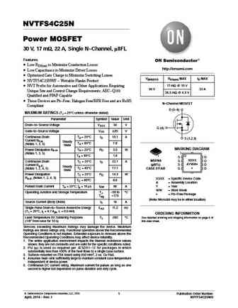
NVTFS4C25N Power MOSFET 30 V, 17 mW, 22 A, Single N-Channel, m8FL Features Low RDS(on) to Minimize Conduction Losses http //onsemi.com Low Capacitance to Minimize Driver Losses Optimized Gate Charge to Minimize Switching Losses V(BR)DSS RDS(on) MAX ID MAX NVTFS4C25NWF - Wettable Flanks Product 17 mW @ 10 V NVT Prefix for Automotive and Other Applications Requiring... See More ⇒
nvtfs4c06n.pdf

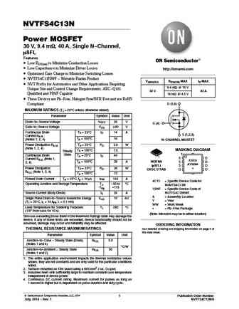
NVTFS4C06N Power MOSFET 30 V, 4.2 mW, 71 A, Single N-Channel, m8FL Features Low RDS(on) to Minimize Conduction Losses Low Capacitance to Minimize Driver Losses http //onsemi.com Optimized Gate Charge to Minimize Switching Losses NVTFS4C06NWF - Wettable Flanks Product V(BR)DSS RDS(on) MAX ID MAX NVT Prefix for Automotive and Other Applications Requiring 4.2 mW @ 1... See More ⇒


Detailed specifications: NVD5803N, NVD5862N, NVD5863NL, NVD5865NL, NVD5867NL, NVD5890N, NVMFD5877NL, NVMFS4841N, IRF830, NVTFS4824N, NVTFS5116PL, NVTFS5811NL, NVTFS5820NL, NVTFS5826NL, SCH1330, SCH1331, SCH1332
Keywords - NVTFS4823N MOSFET specs
NVTFS4823N cross reference
NVTFS4823N equivalent finder
NVTFS4823N pdf lookup
NVTFS4823N substitution
NVTFS4823N replacement
Need a MOSFET replacement? Our guide shows you how to find a perfect substitute by comparing key parameters and specs
History: NVD5890N | IXFA14N60P
🌐 : EN ES РУ

LIST
Last Update
MOSFET: AUB034N10 | AUB033N08BG | AUB026N085 | AUA062N08BG | AUA060N08AG | AUA056N08BGL | AUA039N10 | ASW80R290E | ASW65R120EFD | ASW65R110E
Popular searches
tip31 | tip122 transistor | 2sc1079 | 2sc1815 equivalent | 2sa1220 | 2sa940 | 2sc627 | 2sc680