1N80. Аналоги и основные параметры
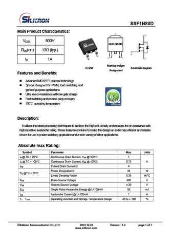
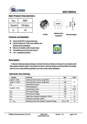
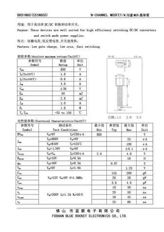
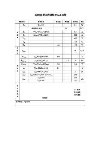
Наименование производителя: 1N80
Тип транзистора: MOSFET
Полярность: N
Предельные значения
Pd ⓘ - Максимальная рассеиваемая мощность: 39 W
|Vds|ⓘ - Максимально допустимое напряжение сток-исток: 800 V
|Vgs|ⓘ - Максимально допустимое напряжение затвор-исток: 30 V
|Id| ⓘ - Максимально допустимый постоянный ток стока: 1 A
Tj ⓘ - Максимальная температура канала: 150 °C
Электрические характеристики
tr ⓘ - Время нарастания: 25 ns
Cossⓘ - Выходная емкость: 20 pf
RDSonⓘ - Сопротивление сток-исток открытого транзистора: 11 Ohm
Тип корпуса: TO-220 TO-251 TO-252 TO-220F TO-220F1
Аналог (замена) для 1N80
- подборⓘ MOSFET транзистора по параметрам
1N80 даташит
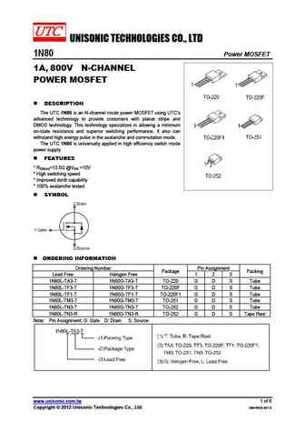
1n80.pdf
UNISONIC TECHNOLOGIES CO., LTD 1N80 Power MOSFET 1A, 800V N-CHANNEL POWER MOSFET DESCRIPTION The UTC 1N80 is an N-channel mode power MOSFET using UTC s advanced technology to provide costomers with planar stripe and DMOS technology. This technology specializes in allowing a minimum on-state resistance and superior switching performance. It also can withstand high energy pu
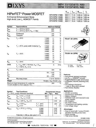
ixfh11n80 ixfm11n80 ixfh13n80 ixfm13n80 ixfh14n80 ixfm14n80 ixfh15n80 ixfm15n80.pdf
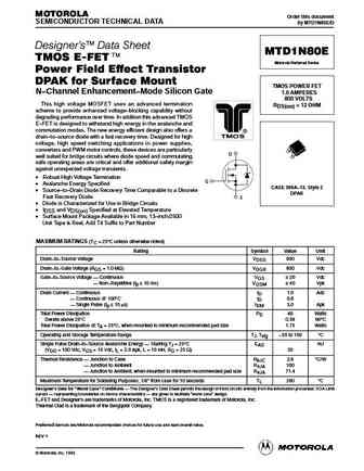
mtd1n80e.pdf
MOTOROLA Order this document SEMICONDUCTOR TECHNICAL DATA by MTD1N80E/D Designer's Data Sheet MTD1N80E TMOS E-FET. Motorola Preferred Device Power Field Effect Transistor DPAK for Surface Mount TMOS POWER FET N Channel Enhancement Mode Silicon Gate 1.0 AMPERES 800 VOLTS This high voltage MOSFET uses an advanced termination RDS(on) = 12 OHM scheme to provide enhanced vo
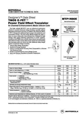
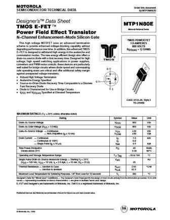
mtp1n80e.pdf
MOTOROLA Order this document SEMICONDUCTOR TECHNICAL DATA by MTP1N80E/D Designer's Data Sheet MTP1N80E TMOS E-FET. Motorola Preferred Device Power Field Effect Transistor N Channel Enhancement Mode Silicon Gate TMOS POWER FET This high voltage MOSFET uses an advanced termination 1.0 AMPERES scheme to provide enhanced voltage blocking capability without 800 VOLTS degra
mtd1n80erev1a.pdf
MOTOROLA Order this document SEMICONDUCTOR TECHNICAL DATA by MTD1N80E/D Designer's Data Sheet MTD1N80E TMOS E-FET. Motorola Preferred Device Power Field Effect Transistor DPAK for Surface Mount TMOS POWER FET N Channel Enhancement Mode Silicon Gate 1.0 AMPERES 800 VOLTS This high voltage MOSFET uses an advanced termination RDS(on) = 12 OHM scheme to provide enhanced vo
mtp1n80erev0ax.pdf
MOTOROLA Order this document SEMICONDUCTOR TECHNICAL DATA by MTP1N80E/D Designer's Data Sheet MTP1N80E TMOS E-FET. Motorola Preferred Device Power Field Effect Transistor N Channel Enhancement Mode Silicon Gate TMOS POWER FET This high voltage MOSFET uses an advanced termination 1.0 AMPERES scheme to provide enhanced voltage blocking capability without 800 VOLTS degra
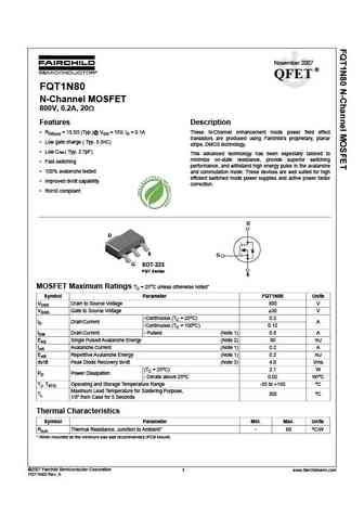
fqt1n80.pdf
November 2007 QFET FQT1N80 N-Channel MOSFET 800V, 0.2A, 20 Features Description RDS(on) = 15.5 (Typ.)@ VGS = 10V, ID = 0.1A These N-Channel enhancement mode power field effect transistors are produced using Fairchild s proprietary, planar Low gate charge ( Typ. 5.5nC) stripe, DMOS technology. Low Crss ( Typ. 2.7pF) This advanced technology has been especiall
fqt1n80tf ws.pdf
November 2007 QFET FQT1N80 N-Channel MOSFET 800V, 0.2A, 20 Features Description RDS(on) = 15.5 (Typ.)@ VGS = 10V, ID = 0.1A These N-Channel enhancement mode power field effect transistors are produced using Fairchild s proprietary, planar Low gate charge ( Typ. 5.5nC) stripe, DMOS technology. Low Crss ( Typ. 2.7pF) This advanced technology has been especiall
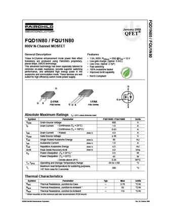
fqd1n80tf fqd1n80tm fqd1n80 fqu1n80 fqu1n80tu.pdf
January 2009 QFET FQD1N80 / FQU1N80 800V N-Channel MOSFET General Description Features These N-Channel enhancement mode power field effect 1.0A, 800V, RDS(on) = 20 @VGS = 10 V transistors are produced using Fairchild s proprietary, Low gate charge ( typical 5.5nC) planar stripe, DMOS technology. Low Crss ( typical 2.7pF) This advanced technology has been especially
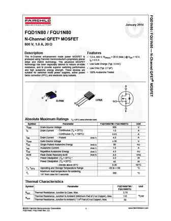
fqu1n80.pdf
January 2014 FQD1N80 / FQU1N80 N-Channel QFET MOSFET 800 V, 1.0 A, 20 Description Features This N-Channel enhancement mode power MOSFET is 1.0 A, 800 V, RDS(on) = 2 0 (Max.) @ VGS = 10 V, produced using Fairchild Semiconductor s proprietary planar ID = 0.5 A stripe and DMOS technology. This advanced MOSFET Low Gate Charge (Typ. 5.5 nC) technology has been espe
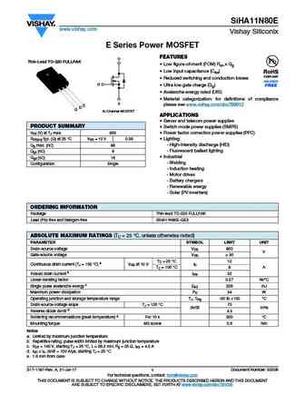
siha11n80e.pdf
SiHA11N80E www.vishay.com Vishay Siliconix E Series Power MOSFET FEATURES D Thin-Lead TO-220 FULLPAK Low figure-of-merit (FOM) Ron x Qg Low input capacitance (Ciss) Reduced switching and conduction losses G Ultra low gate charge (Qg) Avalanche energy rated (UIS) Material categorization for definitions of compliance S please see www.vishay.com/doc?99912
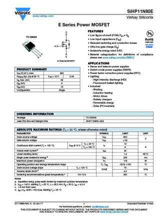
sihp11n80e.pdf
SiHP11N80E www.vishay.com Vishay Siliconix E Series Power MOSFET FEATURES D Low figure-of-merit (FOM) Ron x Qg TO-220AB Low input capacitance (Ciss) Reduced switching and conduction losses G Ultra low gate charge (Qg) Avalanche energy rated (UIS) S Material categorization for definitions of compliance D S G please see www.vishay.com/doc?99912 N-Chann
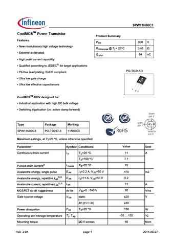
spw11n80c3.pdf
SPW11N80C3 CoolMOSTM Power Transistor Product Summary Features V 800 V DS New revolutionary high voltage technology R @ Tj = 25 C 0.45 DS(on)max Extreme dv/dt rated Q 64 nC g,typ High peak current capability Qualified according to JEDEC1) for target applications PG-TO247-3 Pb-free lead plating; RoHS compliant Ultra low gate charge Ultra low ef
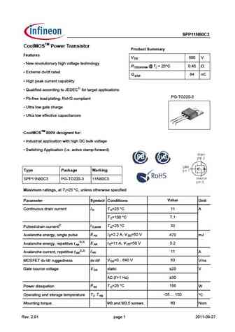
spp11n80c3.pdf
SPP11N80C3 CoolMOSTM Power Transistor Product Summary Features V 800 V DS New revolutionary high voltage technology R @ Tj = 25 C 0.45 DS(on)max Extreme dv/dt rated Q 64 nC g,typ High peak current capability Qualified according to JEDEC1) for target applications PG-TO220-3 Pb-free lead plating; RoHS compliant Ultra low gate charge Ultra low eff
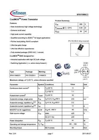
spa11n80c3.pdf
SPA11N80C3 CoolMOSTM Power Transistor Product Summary Features V 800 V DS New revolutionary high voltage technology R @ Tj = 25 C 0.45 DS(on)max Extreme dv/dt rated Q 64 nC g,typ High peak current capability Qualified according to JEDEC1) for target applications Pb-free lead plating; RoHS compliant Ultra low gate charge Ultra low effective capac
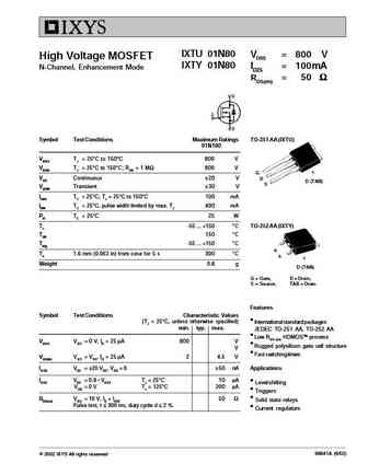
ixtu01n80 ixty01n80.pdf
IXTU 01N80 VDSS = 800 V High Voltage MOSFET IXTY 01N80 ID25 = 100mA N-Channel, Enhancement Mode RDS(on) = 50 Symbol Test Conditions Maximum Ratings TO-251 AA (IXTU) 01N100 VDSS TJ = 25 C to 150 C 800 V VDGR TJ = 25 C to 150 C; RGS = 1 M 800 V G VGS Continuous 20 V D D (TAB) S VGSM Transient 30 V ID25 TC = 25 C; TJ = 25 C to 150 C 100 mA ID
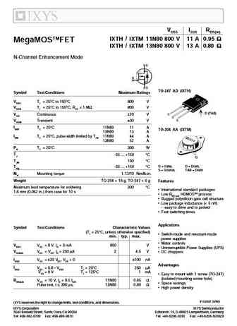
ixth11n80 ixtm11n80 ixth13n80 ixtm13n80.pdf
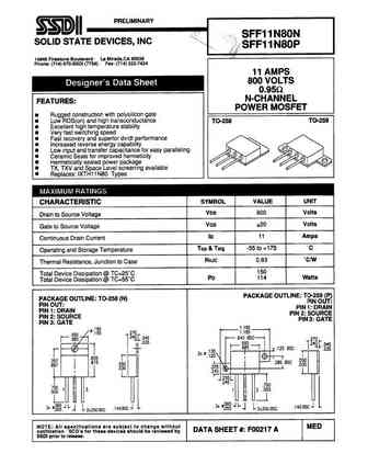
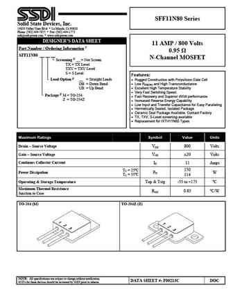
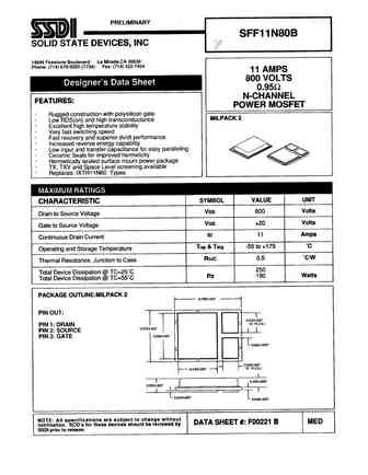
VDSS ID25 RDS(on) IXTH / IXTM 11N80 800 V 11 A 0.95 MegaMOSTMFET IXTH / IXTM 13N80 800 V 13 A 0.80 N-Channel Enhancement Mode TO-247 AD (IXTH) Symbol Test Conditions Maximum Ratings VDSS TJ = 25 C to 150 C 800 V VDGR TJ = 25 C to 150 C; RGS = 1 M 800 V D (TAB) VGS Continuous 20 V VGSM Transient 30 V ID25 TC = 25 C 11N80 11
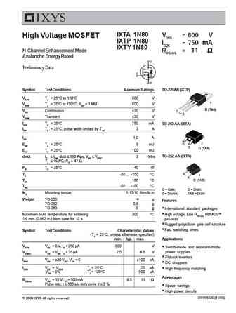
ixta1n80 ixtp1n80 ixty1n80.pdf
IXTA 1N80 VDSS = 800 V High Voltage MOSFET IXTP 1N80 ID25 = 750 mA IXTY 1N80 N-Channel Enhancement Mode RDS(on) = 11 Avalanche Energy Rated Preliminary Data Symbol Test Conditions Maximum Ratings TO-220AB (IXTP) VDSS TJ = 25 C to 150 C 800 V VDGR TJ = 25 C to 150 C; RGS = 1 M 800 V D (TAB) VGS Continuous 20 V G D S VGSM Transient 30 V ID25 T
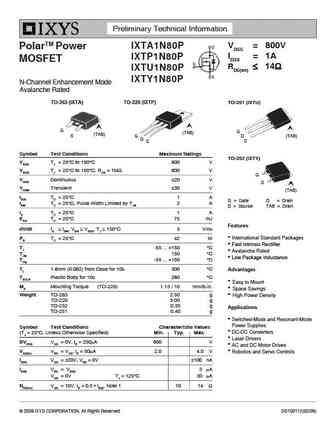
ixta1n80p ixtp1n80p ixtu1n80p ixty1n80p.pdf
Preliminary Technical Information VDSS = 800V IXTA1N80P PolarTM Power ID25 = 1A IXTP1N80P MOSFET RDS(on) 14 IXTU1N80P IXTY1N80P N-Channel Enhancement Mode Avalanche Rated TO-263 (IXTA) TO-220 (IXTP) TO-251 (IXTU) G G (TAB) (TAB) (TAB) S G D D S S Symbol Test Conditions Maximum Ratings TO-252 (IXTY) VDSS TJ = 25 C to 150 C 800 V VD
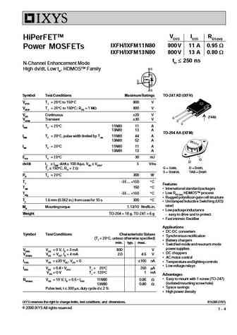
ixfh11n80 ixfh13n80 ixfm11n80 ixfm13n80.pdf
VDSS ID25 RDS(on) HiPerFETTM IXFH/IXFM 11 N80 800 V 11 A 0.95 W Power MOSFETs IXFH/IXFM 13 N80 800 V 13 A 0.80 W trr 250 ns N-Channel Enhancement Mode High dv/dt, Low trr, HDMOSTM Family Symbol Test Conditions Maximum Ratings TO-247 AD (IXFH) VDSS TJ = 25 C to 150 C 800 V VDGR TJ = 25 C to 150 C; RGS = 1 MW 800 V VGS Continuous 20 V (TAB) VGSM Transient 30 V ID25 TC = 2
fqt1n80tf-ws.pdf
ON Semiconductor Is Now To learn more about onsemi , please visit our website at www.onsemi.com onsemi and and other names, marks, and brands are registered and/or common law trademarks of Semiconductor Components Industries, LLC dba onsemi or its affiliates and/or subsidiaries in the United States and/or other countries. onsemi owns the rights to a number of patents, trademarks,
fqd1n80 fqu1n80.pdf
Is Now Part of To learn more about ON Semiconductor, please visit our website at www.onsemi.com Please note As part of the Fairchild Semiconductor integration, some of the Fairchild orderable part numbers will need to change in order to meet ON Semiconductor s system requirements. Since the ON Semiconductor product management systems do not have the ability to manage part nomenclatur
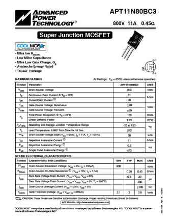
apt11n80bc3g.pdf
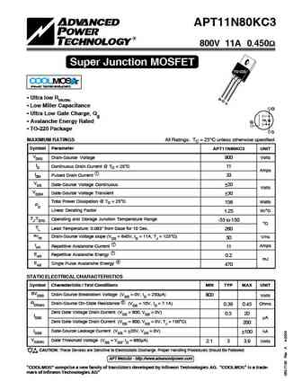
APT11N80BC3 800V 11A 0.45 Super Junction MOSFET TO-247 COOLMOS Power Semiconductors Ultra low RDS(ON) Low Miller Capacitance D Ultra Low Gate Charge, Qg Avalanche Energy Rated G TO-247 Package S MAXIMUM RATINGS All Ratings TC = 25 C unless otherwise specified. Symbol Parameter APT11N80BC3 UNIT VDSS Drain-Source Voltage 800 Volts ID
apt11n80bc3.pdf
APT11N80BC3 800V 11A 0.45 Super Junction MOSFET TO-247 COOLMOS Power Semiconductors Ultra low RDS(ON) Low Miller Capacitance D Ultra Low Gate Charge, Qg Avalanche Energy Rated G TO-247 Package S MAXIMUM RATINGS All Ratings TC = 25 C unless otherwise specified. Symbol Parameter APT11N80BC3 UNIT VDSS Drain-Source Voltage 800 Volts ID
apt11n80kc3.pdf
APT11N80KC3 800V 11A 0.450 Super Junction MOSFET TO-220 COOLMOS Power Semiconductors Ultra low RDS(ON) G D S Low Miller Capacitance D Ultra Low Gate Charge, Qg Avalanche Energy Rated G TO-220 Package S MAXIMUM RATINGS All Ratings TC = 25 C unless otherwise specified. Symbol Parameter APT11N80KC3 UNIT VDSS Drain-Source Voltage 800
apt31n80jc3.pdf
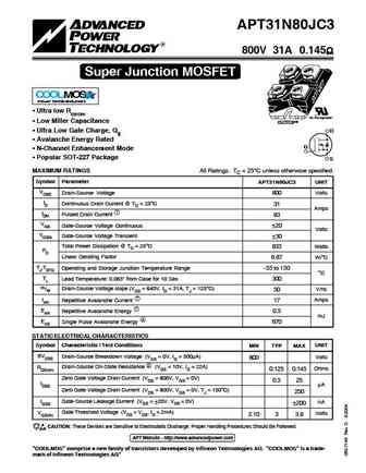
APT31N80JC3 800V 31A 0.145 Super Junction MOSFET COOLMOS Power Semiconductors Ultra low RDS(ON) "UL Recognized" Low Miller Capacitance ISOTOP Ultra Low Gate Charge, Qg D Avalanche Energy Rated G N-Channel Enhancement Mode Popular SOT-227 Package S MAXIMUM RATINGS All Ratings TC = 25 C unless otherwise specified. Symbol Paramete
apt11n80kc3g.pdf
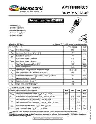
APT11N80KC3 800V 11A 0.450 Super Junction MOSFET TO-220 Ultra Low RDS(ON) Low Miller Capacitance Ultra Low Gate Charge, Qg G D Avalanche Energy Rated S Extreme dv/dt Rated MAXIMUM RATINGS All Ratings TC = 25 C unless otherwise specified. Symbol Parameter APT11N80KC3 UNIT VDSS Drain-Source Voltage 800 Volts ID Continuous Drain Current @ TC = 25 C 1
tsm1n80cw tsm1n80sct.pdf
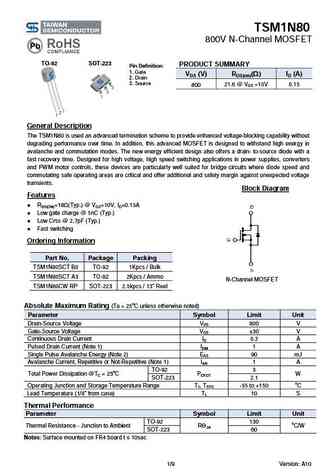
TSM1N80 800V N-Channel MOSFET TO-92 SOT-223 PRODUCT SUMMARY Pin Definition 1. Gate VDS (V) RDS(on)( ) ID (A) 2. Drain 3. Source 21.6 @ VGS =10V 0.15 800 General Description The TSM1N80 is used an advanced termination scheme to provide enhanced voltage-blocking capability without degrading performance over time. In addition, this advanced MOSFET is designed to with
cjd01n80.pdf
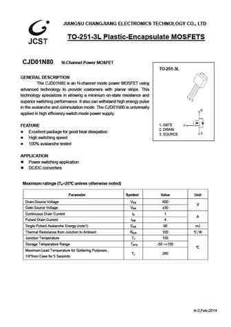
JIANGSU CHANGJIANG ELECTRONICS TECHNOLOGY CO., LTD TO-251-3L Plastic-Encapsulate MOSFETS CJD01N80 N-Channel Power MOSFET TO-251-3L GENERAL DESCRIPTION The CJD01N80 is an N-channel mode power MOSFET using advanced technology to provide costomers with planar stripe. This technology specializes in allowing a minimum on-state resistance and superior switching performance. It also
cju01n80.pdf
JIANGSU CHANGJIANG ELECTRONICS TECHNOLOGY CO., LTD TO-252-2L Plastic-Encapsulate MOSFETS CJU01N80 N-Channel Power MOSFET TO-252-2L GENERAL DESCRIPTION The CJU01N80 is an N-channel mode power MOSFET using advanced technology to provide costomers with planar stripe. This technology specializes in allowing a minimum on-state resistance and superior switching performance. It also
brs1n80.pdf
BRS1N80(CS1N80S) N-CHANNEL MOSFET/N MOS DC/DC Purpose These devices are well suited for high efficiency switching DC/DC converters and switch mode power supplies. , , Features Low gate charge, low crss, fast switching. /Absolute maximum ratings(Ta=25
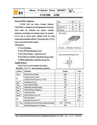
cs1n80 a3h.pdf
Silicon N-Channel Power MOSFET R CS1N80 A3H General Description VDSS 800 V CS1N80 A3H, the silicon N-channel Enhanced ID 1 A PD (TC=25 ) 30 W VDMOSFETs, is obtained by the self-aligned planar Technology RDS(ON)Typ 12 which reduce the conduction loss, improve switching performance and enhance the avalanche energy. The transistor can be used in various power sw
cs1n80 a4h.pdf
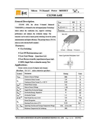
Silicon N-Channel Power MOSFET R CS1N80 A4H General Description VDSS 800 V CS1N80 A4H, the silicon N-channel Enhanced ID 1 A PD (TC=25 ) 30 W VDMOSFETs, is obtained by the self-aligned planar Technology RDS(ON)Typ 12 which reduce the conduction loss, improve switching performance and enhance the avalanche energy. The transistor can be used in various power
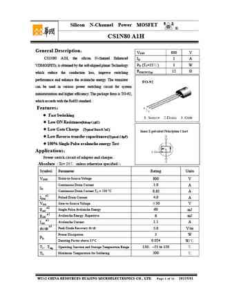
cs1n80 a1h.pdf
Silicon N-Channel Power MOSFET R CS1N80 A1H General Description VDSS 800 V CS1N80 A1H, the silicon N-channel Enhanced ID 1 A PD (TC=25 ) 3 W VDMOSFETs, is obtained by the self-aligned planar Technology RDS(ON)Typ 12 which reduce the conduction loss, improve switching performance and enhance the avalanche energy. The transistor can be used in various power sw
cs1n80.pdf
CS1N80 N PD TC=25 2.1 W 0.02 W/ ID VGS=10V,TC=25 0.2 A ID VGS=10V,TC=100 0.12 A VGS 30 V Tjm +150 Tstg -55 +150 RthJC 60 /W BVDSS VGS=0V,ID=0.25mA 800 V RDS on VGS=10V,ID=0.1A 15.5 20
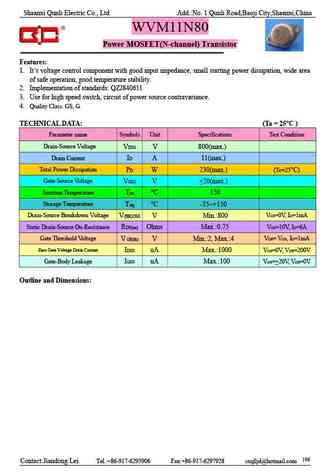
wvm11n80.pdf
Shaanxi Qunli Electric Co., Ltd Add. No. 1 Qunli Road,Baoji City,Shaanxi,China WVM11N80 Power MOSFET(N-channel) Transistor Features 1. It s voltage control component with good input impedance, small starting power dissipation, wide area of safe operation, good temperature stability. 2. Implementation of standards QZJ840611 3. Use for high speed switch, circuit of power source co
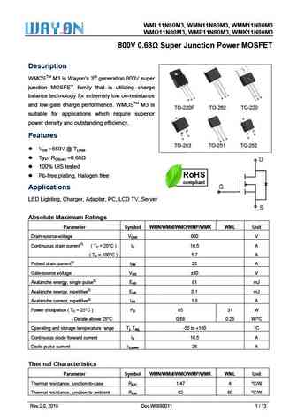
wml11n80m3 wmn11n80m3 wmm11n80m3 wmo11n80m3 wmp11n80m3 wmk11n80m3.pdf
WML11N80M3, W 80M3, WM M3 WMN11N8 MM11N80M WMO1 80M3, WM M3 11N80M3, WMP11N8 MK11N80M 800V 0.68 S T V Super Junction Power MOSFET Descrip ption WMOSTM M3 is Wayo neration 800 M on s 3rd gen 0V super junction MOSFET fa that is utilizing charge M amily S balance te or extremely esistance D echnology fo y low on-re S S G D D G G G T and low ga charge perfo
cs1n80a3h.pdf
Silicon N-Channel Power MOSFET R CS1N80 A3H General Description VDSS 800 V CS1N80 A3H, the silicon N-channel Enhanced ID 1 A PD (TC=25 ) 30 W VDMOSFETs, is obtained by the self-aligned planar Technology RDS(ON)Typ 12 which reduce the conduction loss, improve switching performance and enhance the avalanche energy. The transistor can be used in various power sw
cs1n80a1h.pdf
Silicon N-Channel Power MOSFET R CS1N80 A1H General Description VDSS 800 V CS1N80 A1H, the silicon N-channel Enhanced ID 1 A PD (TC=25 ) 3 W VDMOSFETs, is obtained by the self-aligned planar Technology RDS(ON)Typ 12 which reduce the conduction loss, improve switching performance and enhance the avalanche energy. The transistor can be used in various power sw
cs1n80a4h.pdf
Silicon N-Channel Power MOSFET R CS1N80 A4H General Description VDSS 800 V CS1N80 A4H, the silicon N-channel Enhanced ID 1 A PD (TC=25 ) 30 W VDMOSFETs, is obtained by the self-aligned planar Technology RDS(ON)Typ 12 which reduce the conduction loss, improve switching performance and enhance the avalanche energy. The transistor can be used in various power
sfp024n80c3 sfb021n80c3.pdf
SFP024N80C3,SFB021N80C3 N-MOSFET 80V, 1.9m , 120A Product Summary Features VDS Extremely low on-resistance RDS(on) 80V Qualified according to JEDEC criteria RDS(on) typ. 1.9m Fast switching ID 120A 100% DVDS Tested Applications 100% Avalanche Tested Motor control and drive General purpose applications D G S SFP024N80C3 SFB021N80C3 Package Marking and
sfp024n80i3 sfb021n80i3.pdf
SFP024N80I3,SFB021N80I3 N-MOSFET 80V, 1.9m , 120A Product Summary Features VDS Extremely low on-resistance RDS(on) 80V Qualified according to JEDEC criteria RDS(on) typ. 1.9m Fast switching ID 120A 100% DVDS Tested Applications 100% Avalanche Tested Motor control and drive General purpose applications D G S SFP024N80I3 SFB021N80I3 Package Marking and
siha11n80e.pdf
INCHANGE Semiconductor Isc N-Channel MOSFET Transistor SiHA11N80E FEATURES With TO-220F package Low input capacitance and gate charge Low gate input resistance Reduced switching and conduction losses 100% avalanche tested Minimum Lot-to-Lot variations for robust device performance and reliable operation APPLICATIONS Switching applications ABSOLUTE MAXIMUM RATINGS
apt11n80bc3g.pdf
isc N-Channel MOSFET Transistor APT11N80BC3G FEATURES Drain Current I =11A@ T =25 D C Drain Source Voltage- V =800V(Min) DSS Static Drain-Source On-Resistance R =0.45 (Max) DS(on) 100% avalanche tested Minimum Lot-to-Lot variations for robust device performance and reliable operation DESCRIPTION Designed for use in switch mode power supplies and general pur
spw11n80c3.pdf
INCHANGE Semiconductor isc N-Channel MOSFET Transistor SPW11N80C3 ISPW11N80C3 FEATURES Static drain-source on-resistance RDS(on) 450m Enhancement mode 100% avalanche tested Minimum Lot-to-Lot variations for robust device performance and reliable operation DESCRITION Fast switching ABSOLUTE MAXIMUM RATINGS(T =25 ) a SYMBOL PARAMETER VALUE UNIT V Drain-Sou
spp11n80c3.pdf
INCHANGE Semiconductor Isc N-Channel MOSFET Transistor SPP11N80C3 FEATURES Ultra low effective capacitances Low gate charge Improved transconductance Low gate drive power loss 100% avalanche tested Minimum Lot-to-Lot variations for robust device performance and reliable operation APPLICATIONS Switching applications ABSOLUTE MAXIMUM RATINGS(T =25 ) a SYMBOL PA
spa11n80c3.pdf
INCHANGE Semiconductor isc N-Channel MOSFET Transistor SPA11N80C3 FEATURES New revolutionary high voltage technology Ultra low gate charge High peak current capability Improved transconductance 100% avalanche tested Minimum Lot-to-Lot variations for robust device performance and reliable operation APPLICATIONS Switching applications ABSOLUTE MAXIMUM RATINGS(T =25
Другие IGBT... 9N100, 1N90, 2N90, 3N90, 4N90, 5N90, 6N90, 7N90, 7N65, 2N80, 3N80, 4N80, 5N80, 6N80, 7N80, 8N80, 9N80
History: AO4818B | STP80N70F4
🌐 : EN ES РУ
Список транзисторов
Обновления
MOSFET: AUP060N055 | AUP056N10 | AUP056N08BGL | AUP052N085 | AUP045N12 | AUP039N10 | AUP034N10 | AUP034N06 | AUP033N08BG | AUP026N085 | AUN084N10 | AUN065N10 | AUN063N10 | AUN062N08BG | AUN060N08AG | AUN053N10
Popular searches
c458 transistor | 2sc1775 | 2n1305 | 2sc5242 | irf540 equivalent | mp1620 transistor equivalent | 2sc945 transistor | c2073 transistor
