18N65 datasheet, аналоги, основные параметры
Наименование производителя: 18N65 📄📄
Тип транзистора: MOSFET
Полярность: N
Предельные значения
Pd ⓘ - Максимальная рассеиваемая мощность: 390 W
|Vds|ⓘ - Максимально допустимое напряжение сток-исток: 650 V
|Vgs|ⓘ - Максимально допустимое напряжение затвор-исток: 30 V
|Id| ⓘ - Максимально допустимый постоянный ток стока: 18 A
Tj ⓘ - Максимальная температура канала: 150 °C
Электрические характеристики
tr ⓘ - Время нарастания: 60 ns
Cossⓘ - Выходная емкость: 280 pf
RDSonⓘ - Сопротивление сток-исток открытого транзистора: 0.36 Ohm
Тип корпуса: TO-3P
TO-247
TO-230
📄📄 Копировать
Аналог (замена) для 18N65
- подборⓘ MOSFET транзистора по параметрам
18N65 даташит
..1. Size:176K utc
18n65.pdf 
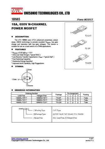
UNISONIC TECHNOLOGIES CO., LTD 18N65 Power MOSFET 18A, 650V N-CHANNEL POWER MOSFET DESCRIPTION The UTC 18N65 uses UTC s advanced proprietary, planar stripe, DMOS technology to provide excellent RDS(ON), low gate charge and operation with low gate voltages. This device is suitable for use as a load switch or in PWM applications. FEATURES * RDS(ON) 0.5 @VGS =
0.1. Size:1015K st
stb18n65m5 std18n65m5.pdf 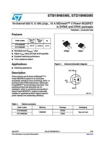
STB18N65M5, STD18N65M5 N-channel 650 V, 0.198 typ., 15 A MDmesh V Power MOSFET in D PAK and DPAK packages Datasheet production data Features VDSS @ RDS(on) Order codes ID TAB TJmax max TAB STB18N65M5 710 V
0.2. Size:563K st
stfu18n65m2.pdf 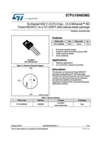
STFU18N65M2 N-channel 650 V, 0.275 typ., 12 A MDmesh M2 Power MOSFET in a TO-220FP ultra narrow leads package Datasheet - production data Features Order code V R max I DS DS(on) D STFU18N65M2 650 V 0.33 12 A Extremely low gate charge Excellent output capacitance (C ) profile oss 100% avalanche tested 3 2 1 Zener-protected TO-220FP Application
0.3. Size:795K st
stf18n65m2.pdf 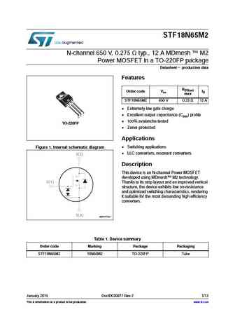
STF18N65M2 N-channel 650 V, 0.275 typ., 12 A MDmesh M2 Power MOSFET in a TO-220FP package Datasheet - production data Features RDS(on) Order code VDS ID max STF18N65M2 650 V 0.33 12 A Extremely low gate charge 3 2 Excellent output capacitance (Coss) profile 1 100% avalanche tested TO-220FP Zener-protected Applications Switching applications F
0.4. Size:525K st
sti18n65m2 stp18n65m2.pdf 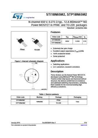
STI18N65M2, STP18N65M2 N-channel 650 V, 0.275 typ., 12 A MDmesh M2 Power MOSFET in I PAK and TO-220 packages Datasheet - production data Features Order code VDS RDS(on) max ID TAB TAB STI18N65M2 650V 0.33 12 A STP18N65M2 3 3 2 2 1 1 Extremely low gate charge I2PAK TO-220 Excellent output capacitance (Coss) profile 100% avalanche tested Zener-prote
0.5. Size:704K st
stl18n65m2.pdf 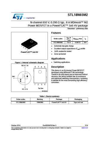
STL18N65M2 N-channel 650 V, 0.290 typ., 8 A MDmesh M2 Power MOSFET in a PowerFLAT 5x6 HV package Datasheet - preliminary data Features VDS @ Order codes TJmax RDS(on) max ID STL18N65M2 715 V 0.365 8 A Extremely low gate charge 1 2 3 Excellent output capacitance (Coss) profile 4 100% avalanche tested PowerFLAT 5x6 HV Zener-protected Applicatio
0.6. Size:1535K st
stl18n65m5.pdf 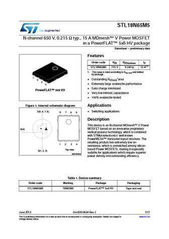
STL18N65M5 N-channel 650 V, 0.215 typ., 15 A MDmesh V Power MOSFET in a PowerFLAT 5x6 HV package Datasheet - preliminary data Features Order code VDS RDS(on)max. ID STL18N65M5 710 V 0.240 15 A(1) 1. The value is rated according to Rthj-case and limited by package. 1 Outstanding RDS(on)*area 2 3 Extremely large avalanche performance 4 Gate charge minimize
0.7. Size:948K st
stf18n65m5 sti18n65m5 stp18n65m5 stw18n65m5.pdf 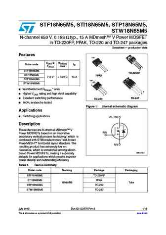
STF18N65M5, STI18N65M5, STP18N65M5, STW18N65M5 N-channel 650 V, 0.198 typ., 15 A MDmesh V Power MOSFET in TO-220FP, I PAK, TO-220 and TO-247 packages Datasheet production data Features TAB VDSS @ RDS(on) Order code ID TJmax max 3 2 1 3 STF18N65M5 2 1 TO-220FP STI18N65M5 I PAK 710 V
0.8. Size:336K ixys
ixfa18n65x2 ixfp18n65x2 ixfh18n65x2.pdf 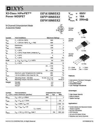
X2-Class HiPerFETTM VDSS = 650V IXFA18N65X2 Power MOSFET ID25 = 18A IXFP18N65X2 RDS(on) 200m IXFH18N65X2 N-Channel Enhancement Mode Avalanche Rated TO-263 (IXFA) G S D (Tab) Symbol Test Conditions Maximum Ratings TO-220 VDSS TJ = 25 C to 150 C 650 V (IXFP) VDGR TJ = 25 C to 150 C, RGS = 1M 650 V VGSS Continuous 30 V VGS
0.9. Size:443K aosemi
aok18n65.pdf 
AOK18N65 650V,18A N-Channel MOSFET General Description Product Summary VDS 750V@150 The AOK18N65 is fabricated using an advanced high voltage MOSFET process that is designed to deliver high ID (at VGS=10V) 18A levels of performance and robustness in popular AC-DC RDS(ON) (at VGS=10V)
0.10. Size:359K aosemi
aotf18n65.pdf 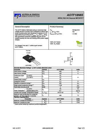
AOTF18N65 650V,18A N-Channel MOSFET General Description Product Summary VDS 750V@150 The AOTF18N65 is fabricated using an advanced high voltage MOSFET process that is designed to deliver high ID (at VGS=10V) 18A levels of performance and robustness in popular AC-DC RDS(ON) (at VGS=10V)
0.11. Size:359K aosemi
aotf18n65l.pdf 
AOTF18N65 650V,18A N-Channel MOSFET General Description Product Summary VDS 750V@150 The AOTF18N65 is fabricated using an advanced high voltage MOSFET process that is designed to deliver high ID (at VGS=10V) 18A levels of performance and robustness in popular AC-DC RDS(ON) (at VGS=10V)
0.12. Size:443K aosemi
aok18n65l.pdf 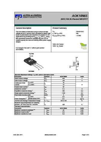
AOK18N65 650V,18A N-Channel MOSFET General Description Product Summary VDS 750V@150 The AOK18N65 is fabricated using an advanced high voltage MOSFET process that is designed to deliver high ID (at VGS=10V) 18A levels of performance and robustness in popular AC-DC RDS(ON) (at VGS=10V)
0.13. Size:253K sisemi
sif18n65c.pdf 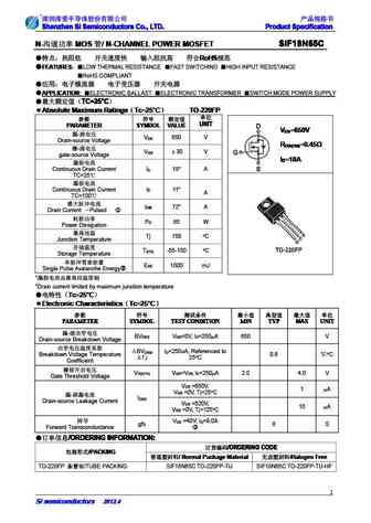
Shenzhen SI Semiconductors Co., LTD. Product Specification Shenzhen SI Semiconductors Co., LTD. Product Specification Shenzhen SI Semiconductors Co., LTD. Product Specification Shenzhen SI Semiconductors Co., LTD. Product Specification N- MOS / N-CHANNEL POWER MOSFET SIF18N65C N- MOS / N-CHANNEL POWER MOSFET SIF18N65C N- MOS / N-CHA
0.14. Size:1247K cn wxdh
f18n65.pdf 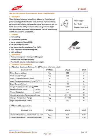
F18N65 18A 650V N-channel Enhancement Mode Power MOSFET 1 Description These N-channel enhanced vdmosfets, is obtained by the self-aligned V DSS = 650V planar technology which reduce the conduction loss, improve switching I = 18.0A D performance and enhance the avalanche energy. Which accords with the RoHS standard. TO-220F provides insulation voltage rated at 2000V R DS(on) TYP)
0.17. Size:467K ruichips
ru18n65p.pdf 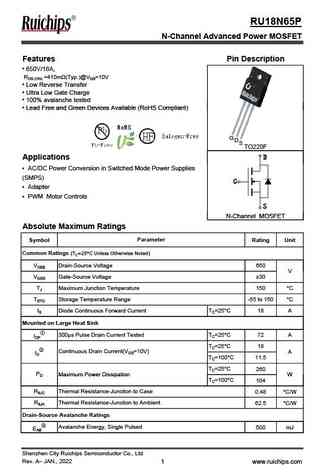
RU18N65P N-Channel Advanced Power MOSFET Features Pin Description 650V/18A, RDS (ON) =410m (Typ.)@VGS=10V Low Reverse Transfer Ultra Low Gate Charge 100% avalanche tested Lead Free and Green Devices Available (RoHS Compliant) Lead Free and Green Devices Available (RoHS Compliant) GD S TO220F D D D D D Applications D pp D AC/DC Power Conversi
0.18. Size:861K jiaensemi
jfpc18n65c jffc18n65c.pdf 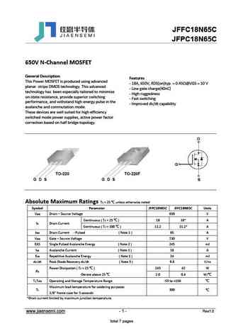
JFFC18N65C JFPC18N65C 650V N-Channel MOSFET General Description Features This Power MOSFET is produced using advanced - 18A, 650V, RDS(on)typ. = 0.45 @VGS = 10 V planar stripe DMOS technology. This advanced - Low gate charge(40nC) technology has been especially tailored to minimize - High ruggedness on-state resistance, provide superior switching - Fast switching perf
0.19. Size:488K jiaensemi
jfpc18n65ci.pdf 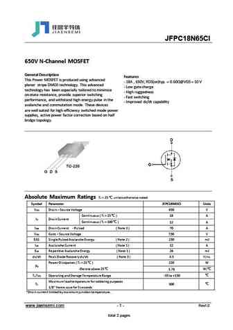
JFPC18N65CI 650V N-Channel MOSFET General Description Features This Power MOSFET is produced using advanced - 18A , 650V, RDS(on)typ. = 0.60 @VGS = 10 V planar stripe DMOS technology. This advanced - Low gate charge technology has been especially tailored to minimize - High ruggedness on-state resistance, provide superior switching - Fast switching performance, and wit
0.20. Size:932K samwin
swf18n65d swt18n65d.pdf 
SW18N65D N-channel Enhanced mode TO-220F/TO-247 MOSFET TO-220F TO-247 BVDSS 650V Features ID 18A High ruggedness RDS(ON) 0.35 Low RDS(ON) (Typ 0.35 )@VGS=10V Low Gate Charge (Typ 79nC) 2 Improved dv/dt Capability 1 1 100% Avalanche Tested 2 2 3 1 3 Application LED , Charger, PC Power 1. Gate 2. Drain 3. Source 3 Gen
0.21. Size:621K samwin
sw18n65d swf18n65d swt18n65d.pdf 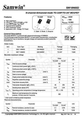
SW18N65D N-channel Enhanced mode TO-220F/TO-247 MOSFET TO-220F TO-247 BVDSS 650V Features ID 18A High ruggedness RDS(ON) 0.35 Low RDS(ON) (Typ 0.35 )@VGS=10V Low Gate Charge (Typ 79nC) 2 Improved dv/dt Capability 1 1 100% Avalanche Tested 2 2 3 1 3 Application LED , Charge, PC Power 1. Gate 2. Drain 3. Source 3 Gene
0.22. Size:708K way-on
wml18n65em wmk18n65em wmm18n65em wmn18n65em wmp18n65em wmo18n65em.pdf 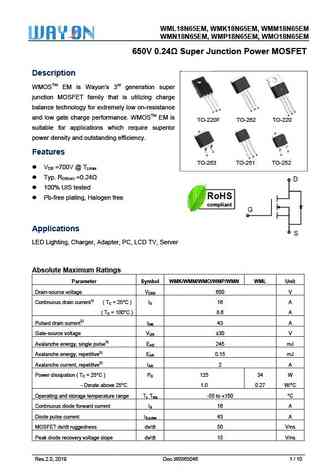
WML18 WMK18N6 8N65EM, W 65EM, WMM18N65EM WMN18 WMP18N6 8N65EM, W 65EM, WMO18N65EM 650V Super Ju MOSFET V 0.24 S unction Power M T Descrip ption WMOSTM EM is Wayon s 3rd generation super W n junction MOSFET fa that is utilizing charge M amily S balance te or extremely esistance echnology fo y low on-re S D D G G G S D G T and low ga ce. WMOSTM EM is
0.23. Size:2574K first semi
fir18n65fg.pdf 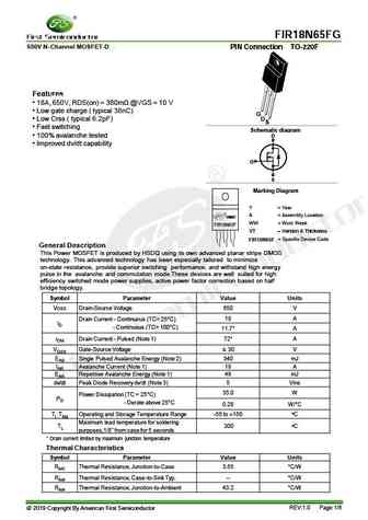
FIR18N65FG 650V N-Channel MOSFET-D . PIN Connection TO-220F Features 18A, 650V, RDS(on) = 380m @VGS = 10 V Low gate charge ( typical 38nC) G D S Low Crss ( typical 6.2pF) Fast switching Schematic diagram 100% avalanche tested D Improved dv/dt capability G S Marking Diagram Y = Year A = Assembly Location YAWWVT WW = Work Week FIR18N65F VT =
0.24. Size:827K cn vbsemi
vbzmb18n65.pdf 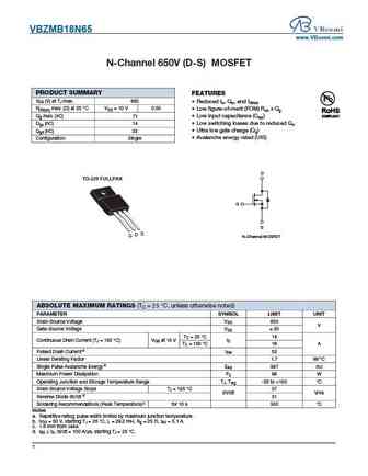
VBZMB18N65 www.VBsemi.com N-Channel 650V (D-S) MOSFET PRODUCT SUMMARY FEATURES VDS (V) at TJ max. 650 Reduced trr, Qrr, and IRRM RDS(on) max. ( ) at 25 C VGS = 10 V 0.50 Low figure-of-merit (FOM) Ron x Qg Qg max. (nC) Low input capacitance (Ciss) 71 Qgs (nC) 14 Low switching losses due to reduced Qrr Ultra low gate charge (Qg) Qgd (nC) 33 Avalanche ener
0.25. Size:378K inchange semiconductor
aok18n65.pdf 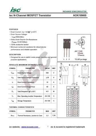
isc N-Channel MOSFET Transistor AOK18N65 FEATURES Drain Current I = 18A@ T =25 D C Drain Source Voltage- V =650V(Min) DSS Static Drain-Source On-Resistance R =0.39 (Max) DS(on) 100% avalanche tested Minimum Lot-to-Lot variations for robust device performance and reliable operation DESCRIPTION Designed for use in switch mode power supplies and general purpos
0.26. Size:252K inchange semiconductor
aotf18n65.pdf 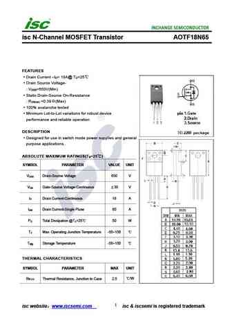
isc N-Channel MOSFET Transistor AOTF18N65 FEATURES Drain Current I = 18A@ T =25 D C Drain Source Voltage- V =650V(Min) DSS Static Drain-Source On-Resistance R =0.39 (Max) DS(on) 100% avalanche tested Minimum Lot-to-Lot variations for robust device performance and reliable operation DESCRIPTION Designed for use in switch mode power supplies and general purpo
0.27. Size:185K inchange semiconductor
stf18n65m5.pdf 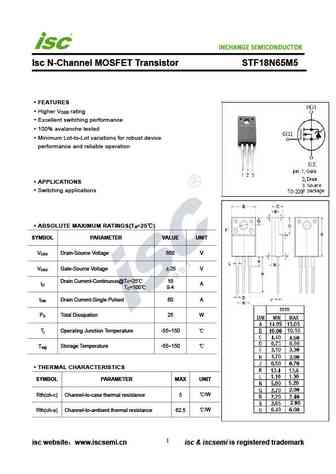
INCHANGE Semiconductor Isc N-Channel MOSFET Transistor STF18N65M5 FEATURES Higher V rating DSS Excellent switching performance 100% avalanche tested Minimum Lot-to-Lot variations for robust device performance and reliable operation APPLICATIONS Switching applications ABSOLUTE MAXIMUM RATINGS(T =25 ) a SYMBOL PARAMETER VALUE UNIT V Drain-Source Voltage 650 V DSS
0.28. Size:208K inchange semiconductor
std18n65m5.pdf 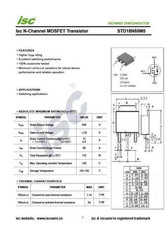
INCHANGE Semiconductor Isc N-Channel MOSFET Transistor STD18N65M5 FEATURES Higher V rating DSS Excellent switching performance 100% avalanche tested Minimum Lot-to-Lot variations for robust device performance and reliable operation APPLICATIONS Switching applications ABSOLUTE MAXIMUM RATINGS(T =25 ) a SYMBOL PARAMETER VALUE UNIT V Drain-Source Voltage 650 V DSS
Другие IGBT... 7N65Z, 7N65K, 8N65, 9N65, 10N65, 10N65Z, 10N65K, 15N65, RFP50N06, 20N65, 22N65, 1N65A, 1N65, 2N65, 2N65L, 2N65Z, 2N65K