15N50. Аналоги и основные параметры
Наименование производителя: 15N50
Тип транзистора: MOSFET
Полярность: N
Предельные значения
Pd ⓘ - Максимальная рассеиваемая мощность: 170 W
|Vds|ⓘ - Максимально допустимое напряжение сток-исток: 500 V
|Vgs|ⓘ - Максимально допустимое напряжение затвор-исток: 30 V
|Id| ⓘ - Максимально допустимый постоянный ток стока: 15 A
Tj ⓘ - Максимальная температура канала: 150 °C
Электрические характеристики
tr ⓘ - Время нарастания: 150 ns
Cossⓘ - Выходная емкость: 250 pf
RDSonⓘ - Сопротивление сток-исток открытого транзистора: 0.26 Ohm
Тип корпуса: TO-220F2
Аналог (замена) для 15N50
- подборⓘ MOSFET транзистора по параметрам
15N50 даташит
15n50.pdf
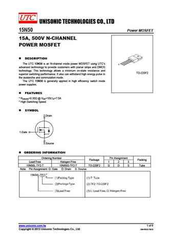
UNISONIC TECHNOLOGIES CO., LTD 15N50 Power MOSFET 15A, 500V N-CHANNEL POWER MOSFET DESCRIPTION The UTC 15N50 is an N-channel mode power MOSFET using UTC s 1 advanced technology to provide customers with planar stripe and DMOS technology. This technology allows a minimum on-state resistance and TO-220F2 superior switching performance. It also can withstand high energy puls

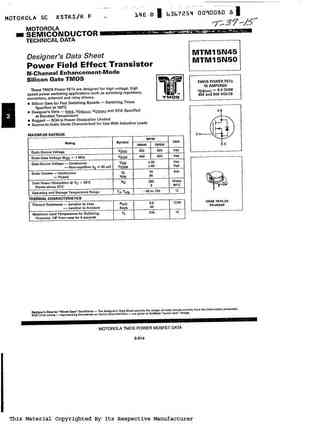
mtm15n45 mtm15n50.pdf
This Material Copyrighted By Its Respective Manufacturer This Material Copyrighted By Its Respective Manufacturer This Material Copyrighted By Its Respective Manufacturer This Material Copyrighted By Its Respective Manufacturer This Material Copyrighted By Its Respective Manufacturer
std15n50m2ag.pdf
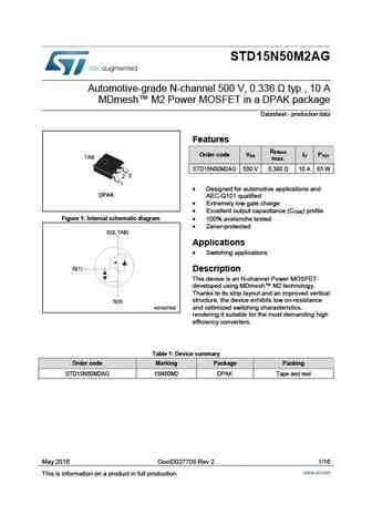
STD15N50M2AG Automotive-grade N-channel 500 V, 0.336 typ., 10 A MDmesh M2 Power MOSFET in a DPAK package Datasheet - production data Features R DS(on) Order code V I P DS D TOT max. STD15N50M2AG 500 V 0.380 10 A 85 W Designed for automotive applications and AEC-Q101 qualified Extremely low gate charge Excellent output capacitance (C ) profile OSS
fdh15n50 fdp15n50 fdb15n50.pdf
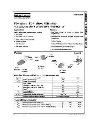
August 2003 FDH15N50 / FDP15N50 / FDB15N50 15A, 500V, 0.38 Ohm, N-Channel SMPS Power MOSFET Applications Features Low Gate Charge Qg results in Simple Drive Switch Mode Power Supplies(SMPS), such as Requirement PFC Boost Improved Gate, Avalanche and High Reapplied dv/dt Two-Switch Forward Converter Ruggedness Single Switch Forward Converter Reduced rDS(ON)
fdh15n50 fdp15n50.pdf

August 2003 FDH15N50 / FDP15N50 / FDB15N50 15A, 500V, 0.38 Ohm, N-Channel SMPS Power MOSFET Applications Features Low Gate Charge Qg results in Simple Drive Switch Mode Power Supplies(SMPS), such as Requirement PFC Boost Improved Gate, Avalanche and High Reapplied dv/dt Two-Switch Forward Converter Ruggedness Single Switch Forward Converter Reduced rDS(ON)
sihp15n50e.pdf
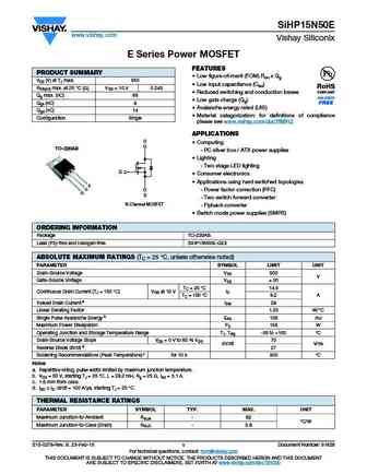
SiHP15N50E www.vishay.com Vishay Siliconix E Series Power MOSFET FEATURES PRODUCT SUMMARY Low figure-of-merit (FOM) Ron x Qg VDS (V) at TJ max. 550 Low input capacitance (Ciss) RDS(on) max. at 25 C ( ) VGS = 10 V 0.243 Reduced switching and conduction losses Qg max. (nC) 66 Low gate charge (Qg) Qgs (nC) 8 Avalanche energy rated (UIS) Qgd (nC) 14 Materi
siha15n50e.pdf
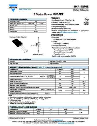
SiHA15N50E www.vishay.com Vishay Siliconix E Series Power MOSFET FEATURES PRODUCT SUMMARY Low figure-of-merit (FOM) Ron x Qg VDS (V) at TJ max. 550 Low input capacitance (Ciss) RDS(on) max. at 25 C ( ) VGS = 10 V 0.243 Reduced switching and conduction losses Qg max. (nC) 66 Low gate charge (Qg) Qgs (nC) 8 Avalanche energy rated (UIS) Qgd (nC) 14 Materi
sihb15n50e.pdf
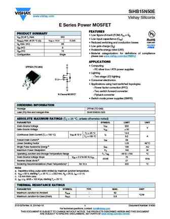
SiHB15N50E www.vishay.com Vishay Siliconix E Series Power MOSFET FEATURES PRODUCT SUMMARY Low figure-of-merit (FOM) Ron x Qg VDS (V) at TJ max. 550 Low input capacitance (Ciss) RDS(on) max. at 25 C ( ) VGS = 10 V 0.243 Reduced switching and conduction losses Qg max. (nC) 66 Low gate charge (Qg) Qgs (nC) 8 Avalanche energy rated (UIS) Qgd (nC) 14 Materi
ixta15n50l2.pdf
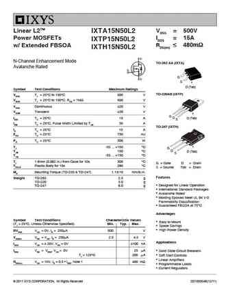
Linear L2TM VDSS = 500V IXTA15N50L2 Power MOSFETs ID25 = 15A IXTP15N50L2 RDS(on) 480m w/ Extended FBSOA IXTH15N50L2 N-Channel Enhancement Mode TO-263 AA (IXTA) Avalanche Rated G S D (Tab) Symbol Test Conditions Maximum Ratings TO-220AB (IXTP) VDSS TJ = 25 C to 150 C 500 V VDGR TJ = 25 C to 150 C, RGS = 1M 500 V VGSS Continuous 20 V
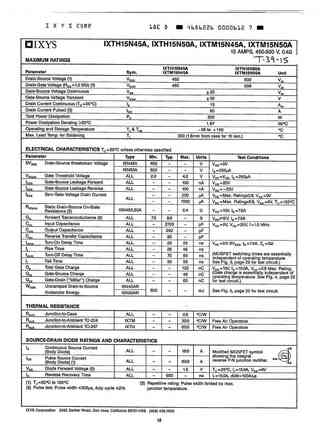
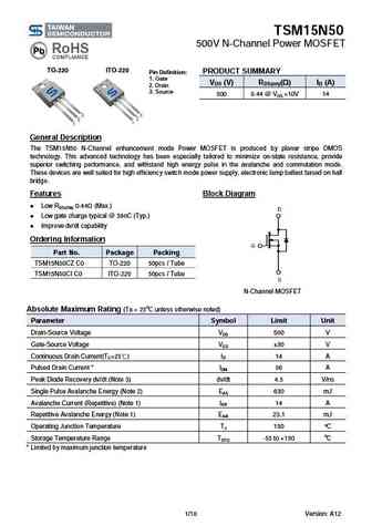
ixth15n50l2-ixtp15n50l2.pdf
Linear L2TM Power VDSS = 500V IXTH15N50L2 MOSFET w/Extended ID25 = 15A IXTP15N50L2 RDS(on) 480m FBSOA N-Channel Enhancement Mode Avalanche Rated TO-220 (IXTP) Symbol Test Conditions Maximum Ratings VDSS TJ = 25 C to 150 C 500 V G (TAB) D VDGR TJ = 25 C to 150 C, RGS = 1M 500 V S VGSS Continuous 20 V TO-247 (IXTH) VGSM Transient 30
fdb15n50.pdf

Is Now Part of To learn more about ON Semiconductor, please visit our website at www.onsemi.com Please note As part of the Fairchild Semiconductor integration, some of the Fairchild orderable part numbers will need to change in order to meet ON Semiconductor s system requirements. Since the ON Semiconductor product management systems do not have the ability to manage part nomenclatur
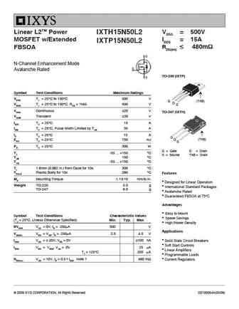
tsm15n50ci.pdf
TSM15N50 500V N-Channel Power MOSFET TO-220 ITO-220 PRODUCT SUMMARY Pin Definition 1. Gate VDS (V) RDS(on)( ) ID (A) 2. Drain 3. Source 500 0.44 @ VGS =10V 14 General Description The TSM15N50 N-Channel enhancement mode Power MOSFET is produced by planar stripe DMOS technology. This advanced technology has been especially tailored to minimize on-state resistance, pro
kf15n50n.pdf
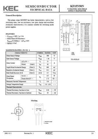
KF15N50N SEMICONDUCTOR N CHANNEL MOS FIELD TECHNICAL DATA EFFECT TRANSISTOR General Description A This planar stripe MOSFET has better characteristics, such as fast Q B N O K switching time, low on resistance, low gate charge and excellent DIM MILLIMETERS avalanche characteristics. It is mainly suitable for switching mode _ A + 15.60 0.20 _ B 4.80 + 0.20 power supplies. _
mtn15n50fp.pdf
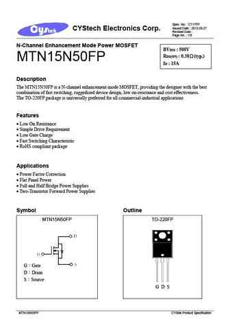
Spec. No. C717FP Issued Date 2013.08.27 CYStech Electronics Corp. Revised Date Page No. 1/8 N-Channel Enhancement Mode Power MOSFET BVDSS 500V RDS(ON) 0.38 (typ.) MTN15N50FP ID 15A Description The MTN15N50FP is a N-channel enhancement-mode MOSFET, providing the designer with the best combination of fast switching, ruggedized device design, low on-resistance
mtn15n50f3.pdf

Spec. No. C717F3 Issued Date 2010.08.03 CYStech Electronics Corp. Revised Date Page No. 1/11 N-Channel Enhancement Mode Power MOSFET BVDSS 500V RDS(ON) 0.38 (typ.) MTN15N50F3 ID 15A Description The MTN15N50F3 is a N-channel enhancement-mode MOSFET, providing the designer with the best combination of fast switching, ruggedized device design, low on-resistanc
mtn15n50e3.pdf
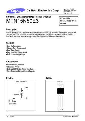
Spec. No. C717E3 Issued Date 2010.08.03 CYStech Electronics Corp. Revised Date Page No. 1/10 N-Channel Enhancement Mode Power MOSFET BVDSS 500V RDS(ON) 0.38 (typ.) MTN15N50E3 ID 15A Description The MTN15N50E3 is a N-channel enhancement-mode MOSFET, providing the designer with the best combination of fast switching, ruggedized device design, low on-resistanc
brfl15n50.pdf
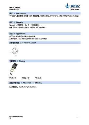
BRFL15N50 Rev.A Sep.-2017 DATA SHEET / Descriptions TO-220FL N MOS N-CHANNEL MOSFET in a TO-220FL Plastic Package. / Features R C DS(on) rss Low RDS(on),low gate charge, low Crss, fast switching. / Applications D Automoti
cs15n50 a8r.pdf
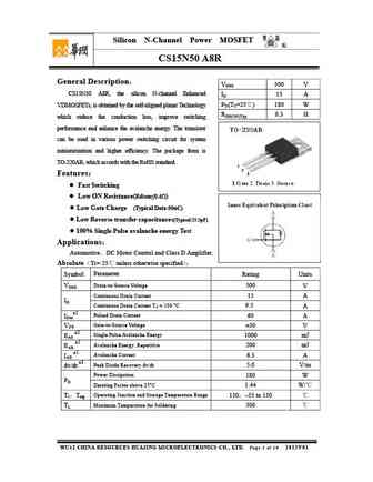
Silicon N-Channel Power MOSFET R CS15N50 A8R General Description VDSS 500 V CS15N50 A8R, the silicon N-channel Enhanced ID 15 A PD(TC=25 ) 180 W VDMOSFETs, is obtained by the self-aligned planar Technology RDS(ON)Typ 0.3 which reduce the conduction loss, improve switching performance and enhance the avalanche energy. The transistor can be used in various pow
cs15n50f a9r.pdf

Silicon N-Channel Power MOSFET R CS15N50F A9R General Description VDSS 500 V CS15N50F A9R, the silicon N-channel Enhanced VDMOSFETs, ID 15 A PD(TC=25 ) 70 W is obtained by the self-aligned planar Technology which reduce RDS(ON)Typ 0.3 the conduction loss, improve switching performance and enhance the avalanche energy. The transistor can be used in various
cm15n50.pdf
R C1N0 M55 www.jdsemi.cn ShenZhen Jingdao Electronic Co.,Ltd. POWER MOSFET 500V N-Channel VDMOS RoHS 1 2 3
kdb15n50.pdf
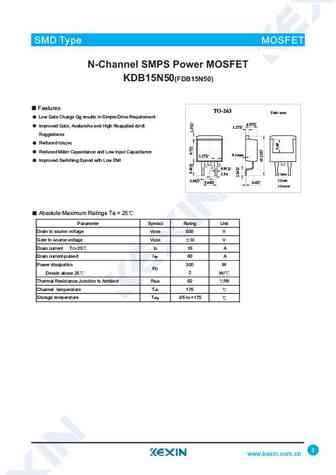
SMD Type MOSFET N-Channel SMPS Power MOSFET KDB15N50(FDB15N50) Features TO-263 Unit mm Low Gate Charge Qg results in Simple Drive Requirement +0.2 4.57-0.2 +0.1 Improved Gate, Avalanche and High Reapplied dv/dt 1.27-0.1 Ruggedness Reduced rDS(ON) Reduced Miller Capacitance and Low Input Capacitance +0.1 0.1max 1.27-0.1 Improved Switching Speed with Low EMI +0.1 0.81-0.1 2.
ms15n50.pdf
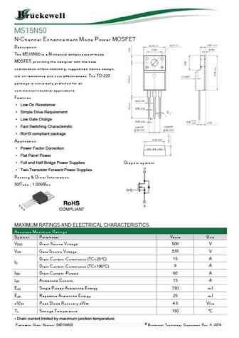
MS15N50 N-Channel Enhancement Mode Power MOSFET Description The MS15N50 is a N-channel enhancement-mode MOSFET, providing the designer with the best combination of fast switching, ruggedized device design, low on-resistance and cost effectiveness. The TO-220 package is universally preferred for all commercial-industrial applications Features Low On Resistance Simpl
af15n50.pdf
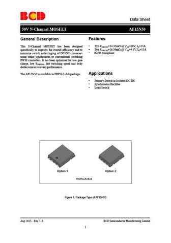
Data Sheet 50V N-Channel MOSFET AF15N50 Features General Description Typ RDS(ON)=14.32m @ VGS=10V, ID=15A This N-Channel MOSFET has been designed Typ RDS(ON)=16.36m @ VGS=4.5V, ID=15A specifically to improve the overall efficiency and to RoHS Compliant minimize switch node ringing of DC-DC converters using either synchronous or conventional switching PWM
bl15n50-p bl15n50-a bl15n50-f.pdf
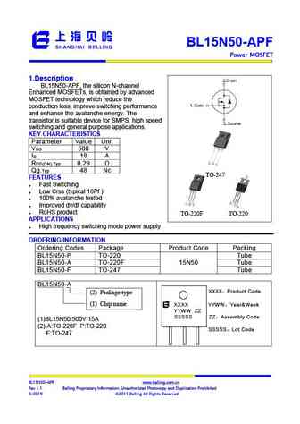
BL15N50-APF Power MOSFET 1.Description Step-Down Converter BL15N50-APF, the silicon N-channel , Enhanced MOSFETs, is obtained by advanced MOSFET technology which reduce the conduction loss, improve switching performance and enhance the avalanche energy. The transistor is suitable device for SMPS, high speed switching and general purpose applications. KEY CHARACTERISTICS
ptp15n50 pta15n50.pdf
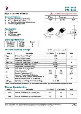
PTP15N50 PTA15N50 500V N-Channel MOSFET General Features BVDSS RDS(ON),typ. ID Proprietary New Planar Technology 500V 0.33 15A RDS(ON),typ.=0.33 @VGS=10V Low Gate Charge Minimize Switching Loss Fast Recovery Body Diode Applications Adaptor TV Main Power SMPS Power Supply LCD Panel Power Ordering Information Part Number Package Bran
swmn15n50d.pdf
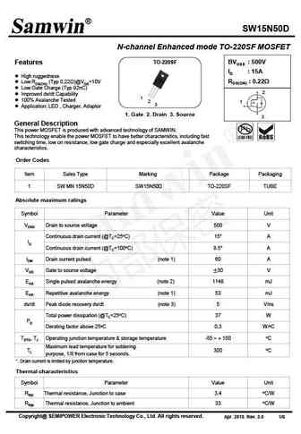
SW15N50D N-channel Enhanced mode TO-220SF MOSFET TO-220SF BVDSS 500V Features ID 15A High ruggedness RDS(ON) 0.22 Low RDS(ON) (Typ 0.22 )@VGS=10V Low Gate Charge (Typ 92nC) 2 Improved dv/dt Capability 1 100% Avalanche Tested 2 1 3 Application LED , Charger, Adaptor 1. Gate 2. Drain 3. Source 3 General Description This
swf15n50.pdf
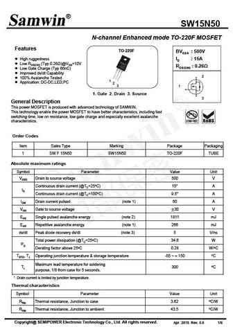
SW15N50 N-channel Enhanced mode TO-220F MOSFET Features TO-220F BVDSS 500V High ruggedness ID 15A Low RDS(ON) (Typ 0.26 )@VGS=10V RDS(ON) 0.26 Low Gate Charge (Typ 66nC) Improved dv/dt Capability 2 100% Avalanche Tested 1 Application DC-DC,LED,PC 2 3 1 1. Gate 2. Drain 3. Source 3 General Description This power MOSFET is
swf15n50da.pdf
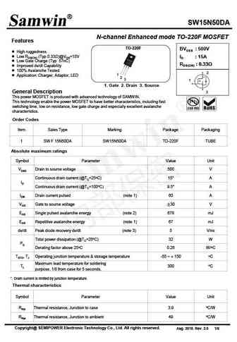
SW15N50DA N-channel Enhanced mode TO-220F MOSFET Features TO-220F BVDSS 500V High ruggedness Low RDS(ON) (Typ 0.33 )@VGS=10V ID 15A Low Gate Charge (Typ 57nC) RDS(ON) 0.33 Improved dv/dt Capability 100% Avalanche Tested 2 1 Application Charger, Adaptor, LED 2 3 1 1. Gate 2. Drain 3. Source General Description 3 This p
wvm15n50.pdf
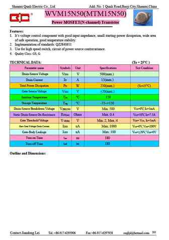
Shaanxi Qunli Electric Co., Ltd Add. No. 1 Qunli Road,Baoji City,Shaanxi,China WVM15N50(MTM15N50) Power MOSFET(N-channel) Transistor Features 1. It s voltage control component with good input impedance, small starting power dissipation, wide area of safe operation, good temperature stability. 2. Implementation of standards QZJ840611 3. Use for high speed switch, circuit of powe
tman15n50.pdf
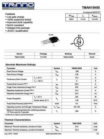
TMAN15N50 N-channel MOSFET Features BVDSS ID RDS(on) Low gate charge 500V 14.2A
tmp15n50 tmpf15n50.pdf
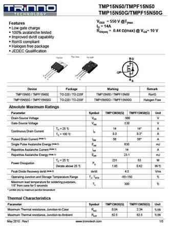
TMP15N50/TMPF15N50 TMP15N50G/TMPF15N50G VDSS = 550 V @Tjmax Features ID = 14A Low gate charge RDS(on) = 0.44 W(max) @ VGS= 10 V 100% avalanche tested Improved dv/dt capability RoHS compliant Halogen free package JEDEC Qualification D G S Device Package Marking Remark TMP15N50 / TMPF15N50 TO-220 / TO-220F TMP15N50 / TMPF15N50 RoHS TMP15N50G / TMPF15N50G
wmk15n50d1b wml15n50d1b.pdf
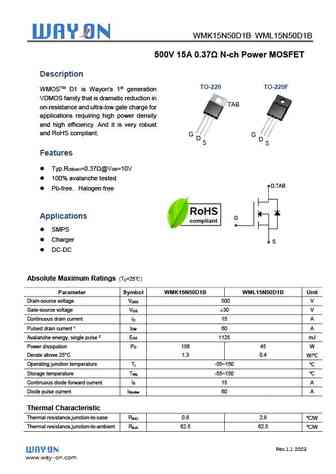
WMK15N50D1B WML15N50D1B 500V 15A 0.37 N-ch Power MOSFET Description TO-220 TO-220F WMOSTM D1 is Wayon s 1st generation VDMOS family that is dramatic reduction in TAB on-resistance and ultra-low gate charge for applications requiring high power density and high efficiency. And it is very robust and RoHS compliant. G G D D S S Features Typ.R =0.37 @V
cs15n50fa9r.pdf
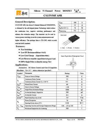
Silicon N-Channel Power MOSFET R CS15N50F A9R General Description VDSS 500 V CS15N50F A9R, the silicon N-channel Enhanced VDMOSFETs, ID 15 A PD(TC=25 ) 70 W is obtained by the self-aligned planar Technology which reduce RDS(ON)Typ 0.3 the conduction loss, improve switching performance and enhance the avalanche energy. The transistor can be used in various
cs15n50f cs15n50p.pdf
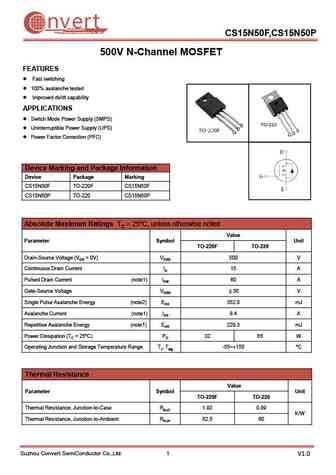
nvert Suzhou Convert Semiconductor Co ., Ltd. CS15N50F,CS15N50P 500V N-Channel MOSFET FEATURES Fast switching 100% avalanche tested Improved dv/dt capability APPLICATIONS Switch Mode Power Supply (SMPS) Uninterruptible Power Supply (UPS) Power Factor Correction (PFC) Device Marking and Package Information Device Package Marking CS15N50F TO-220F CS15N50F CS
jmpc15n50bj.pdf
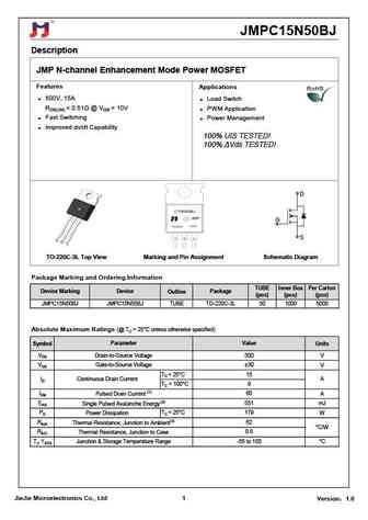
JMPC15N50BJ Description JMP N-channel Enhancement Mode Power MOSFET Features Applications 500V, 15A Load Switch RDS(ON)
jmpf15n50bj.pdf
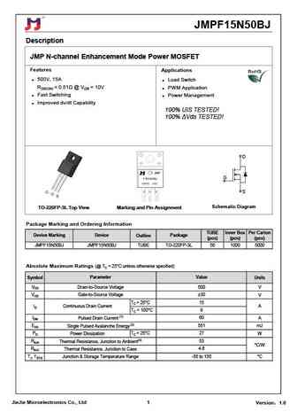
JMPF15N50BJ Description JMP N-channel Enhancement Mode Power MOSFET Features Applications 500V, 15A Load Switch RDS(ON)
se15n50fra.pdf
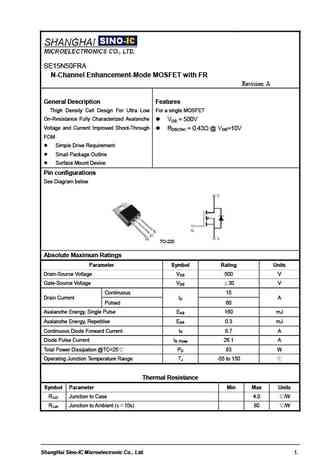
SE15N50FRA N-Channel Enhancement-Mode MOSFET with FR Revision A General Description Features Thigh Density Cell Design For Ultra Low For a single MOSFET On-Resistance Fully Characterized Avalanche VDS = 500V Voltage and Current Improved Shoot-Through RDS(ON) = 0.43 @ VGS=10V FOM Simple Drive Requirement Small Package Outline Surface Mount Device
hm15n50 hm15n50f.pdf
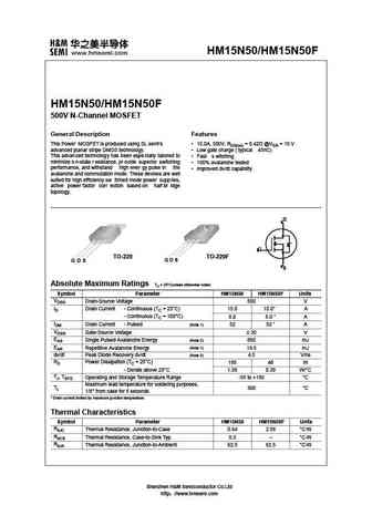
HM15N50/HM15N50F HM15N50/HM15N50F 500V N-Channel MOSFET General Description Features This Power MOSFET is produced using SL semi s 15.0A, 500V, RDS(on) = 0.42 @VGS = 10 V advanced planar stripe DMOS technology. Low gate charge ( typical 45nC) This advanced technology has been espe cially tailored to Fast s witching minimize o n-state r esistance, pr ovide superior switc
fxn15n50f.pdf
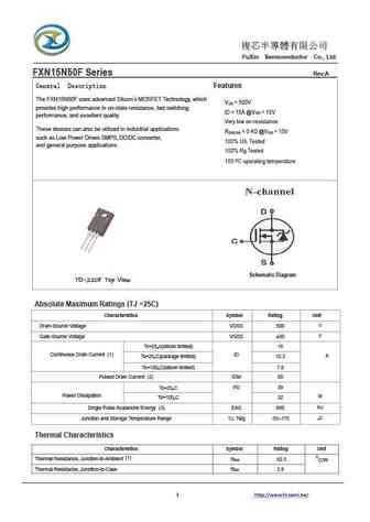
FuXin Semiconductor Co., Ltd. FXN15N50F Series Rev.A General Description Features The FXN15N50F uses advanced Silicon s MOSFET Technology, which V = 500V DS provides high performance in on-state resistance, fast switching ID = 15A @V = 10V GS performance, and excellent quality. Very low on-resistance These devices can also be utilized in industrial a
fdh15n50.pdf
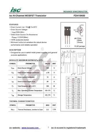
isc N-Channel MOSFET Transistor FDH15N50 FEATURES Drain Current I = 15A@ T =25 D C Drain Source Voltage- V =500V(Min) DSS Static Drain-Source On-Resistance R = 0.38 (Max) DS(on) 100% avalanche tested Minimum Lot-to-Lot variations for robust device performance and reliable operation DESCRIPTION Designed for use in switch mode power supplies and general purpo
Другие MOSFET... 4N60K , 8N50H , 9N50 , 10N50 , 11N50 , 12N50 , 13N50 , 14N50 , 2N7000 , 16N50 , 18N50 , 24N50 , 26N50 , UF830 , UF830Z , UF840 , UK3568 .
🌐 : EN ES РУ

Список транзисторов
Обновления
MOSFET: 2N7002KM | 2N7002KH | AON5802 | AOSS62934 | AOSN21319C | AONS66966 | AONR62992 | AON7400B | AON6578 | AO3480C | AO3400C | HAF1008S | HAF1008L | EMZB08P03H | CS30N20FA9R | AOT66613L
Popular searches
bdx53c | k3563 | d882p | 2sb1560 | 2n1304 | 2sa979 | 2sc4793 | d965