Аналоги 1N50. Основные параметры
Наименование производителя: 1N50
Тип транзистора: MOSFET
Полярность: N
Pd ⓘ - Максимальная рассеиваемая мощность: 40 W
|Vds|ⓘ - Предельно допустимое напряжение сток-исток: 500 V
|Vgs|ⓘ - Предельно допустимое напряжение затвор-исток: 30 V
|Id| ⓘ - Максимально допустимый постоянный ток стока: 1.3 A
Tj ⓘ - Максимальная температура канала: 150 °C
tr ⓘ - Время нарастания: 13 ns
Cossⓘ - Выходная емкость: 30 pf
Rds ⓘ - Сопротивление сток-исток открытого транзистора: 4.6 Ohm
Тип корпуса: TO-220
Аналог (замена) для 1N50
1N50 даташит
1n50.pdf
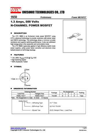
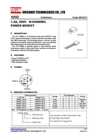
UNISONIC TECHNOLOGIES CO., LTD 1N50 Power MOSFET Preliminary 1.3 Amps, 500 Volts N-CHANNEL POWER MOSFET DESCRIPTION The UTC 1N50 is an N-channel mode power MOSFET using UTC s advanced technology to provide customers with planar stripe 1 TO-220 and DMOS technology. This technology allows a minimum on-state resistance and superior switching performance. It also can withstand
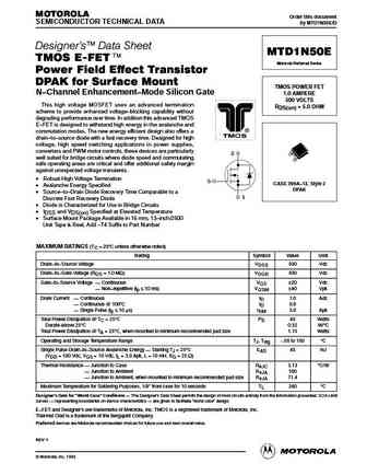
mtd1n50erev1.pdf
MOTOROLA Order this document SEMICONDUCTOR TECHNICAL DATA by MTD1N50E/D Designer's Data Sheet MTD1N50E TMOS E-FET. Motorola Preferred Device Power Field Effect Transistor DPAK for Surface Mount TMOS POWER FET N Channel Enhancement Mode Silicon Gate 1.0 AMPERE 500 VOLTS This high voltage MOSFET uses an advanced termination RDS(on) = 5.0 OHM scheme to provide enhanced vol
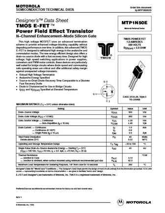
mtp1n50erev1x.pdf
MOTOROLA Order this document SEMICONDUCTOR TECHNICAL DATA by MTP1N50E/D Designer's Data Sheet MTP1N50E TMOS E-FET. Motorola Preferred Device Power Field Effect Transistor N Channel Enhancement Mode Silicon Gate TMOS POWER FET This high voltage MOSFET uses an advanced termination 1.0 AMPERES scheme to provide enhanced voltage blocking capability without 500 VOLTS degra
mtd1n50e.pdf
MOTOROLA Order this document SEMICONDUCTOR TECHNICAL DATA by MTD1N50E/D Designer's Data Sheet MTD1N50E TMOS E-FET. Motorola Preferred Device Power Field Effect Transistor DPAK for Surface Mount TMOS POWER FET N Channel Enhancement Mode Silicon Gate 1.0 AMPERE 500 VOLTS This high voltage MOSFET uses an advanced termination RDS(on) = 5.0 OHM scheme to provide enhanced vol
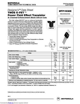
mtp1n50e.pdf
MOTOROLA Order this document SEMICONDUCTOR TECHNICAL DATA by MTP1N50E/D Designer's Data Sheet MTP1N50E TMOS E-FET. Motorola Preferred Device Power Field Effect Transistor N Channel Enhancement Mode Silicon Gate TMOS POWER FET This high voltage MOSFET uses an advanced termination 1.0 AMPERES scheme to provide enhanced voltage blocking capability without 500 VOLTS degra
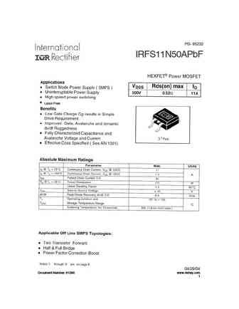
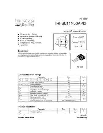
irfs11n50apbf.pdf
PD- 95232 IRFS11N50APbF Lead-Free 04/29/04 Document Number 91286 www.vishay.com 1 IRFS11N50APbF Document Number 91286 www.vishay.com 2 IRFS11N50APbF Document Number 91286 www.vishay.com 3 IRFS11N50APbF Document Number 91286 www.vishay.com 4 IRFS11N50APbF Document Number 91286 www.vishay.com 5 IRFS11N50APbF Document Number 91286 www.vishay.com 6 IRFS11N50APb
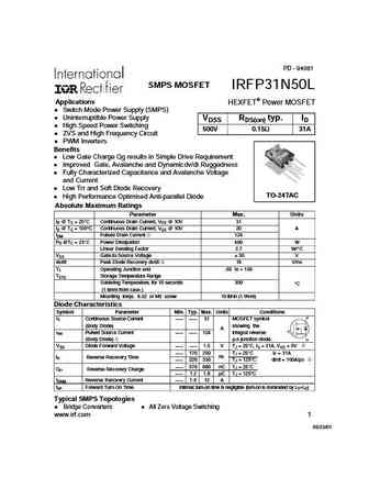
irfp31n50l.pdf
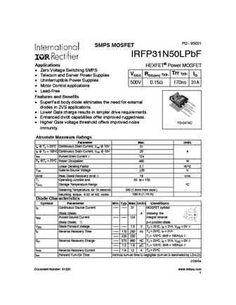
PD - 94081 SMPS MOSFET IRFP31N50L Applications HEXFET Power MOSFET Switch Mode Power Supply (SMPS) UninterruptIble Power Supply VDSS RDS(on) typ. ID High Speed Power Switching 500V 0.15 31A ZVS and High Frequency Circuit PWM Inverters Benefits Low Gate Charge Qg results in Simple Drive Requirement Improved Gate, Avalanche and Dynamicdv/dt Ruggedness Fully Characterize
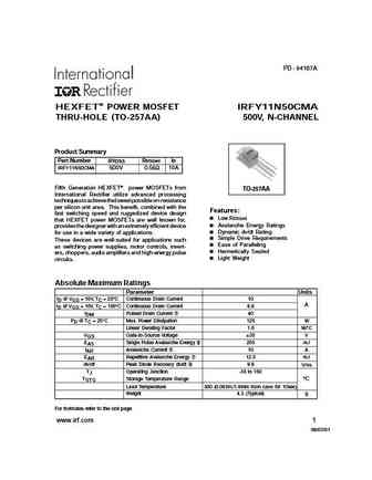
irfy11n50cma.pdf
PD - 94167A HEXFET POWER MOSFET IRFY11N50CMA THRU-HOLE (TO-257AA) 500V, N-CHANNEL Product Summary Part Number BVDSS RDS(on) ID IRFY11N50CMA 500V 0.56 10A Fifth Generation HEXFET power MOSFETs from TO-257AA International Rectifier utilize advanced processing techniques to achieve the lowest possible on-resistance per silicon unit area. This benefit, combined with the Feature
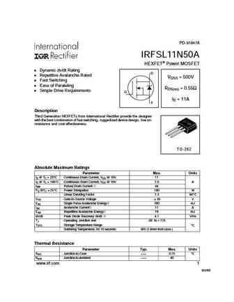
irfsl11n50a.pdf
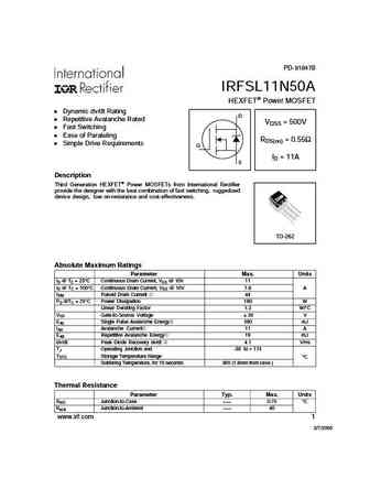
PD- 91847A IRFSL11N50A HEXFET Power MOSFET Dynamic dv/dt Rating D Repetitive Avalanche Rated VDSS = 500V Fast Switching Ease of Paraleling RDS(on) = 0.55 Simple Drive Requirements G ID = 11A S Description Third Generation HEXFETs from International Rectifier provide the designer with the best combination of fast switching, ruggedized device design, low on- resistance
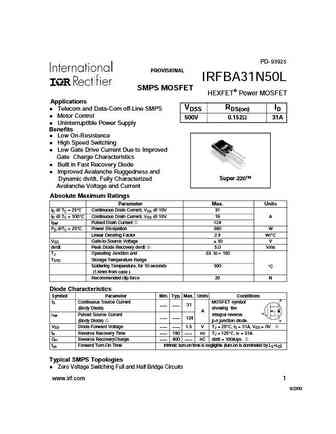
irfba31n50l.pdf
PD- 93925 PROVISIONAL IRFBA31N50L SMPS MOSFET HEXFET Power MOSFET Applications VDSS RDS(on) ID Telecom and Data-Com off-Line SMPS Motor Control 500V 0.152 31A UninterruptIble Power Supply Benefits Low On-Resistance High Speed Switching Low Gate Drive Current Due to Improved Gate Charge Characteristics Built in Fast Recovery Diode Improved Avalanche Ruggedness and
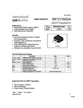
irfs11n50a.pdf
PD- 93797 SMPS MOSFET IRFS11N50A HEXFET Power MOSFET Applications VDSS Rds(on) max ID Switch Mode Power Supply ( SMPS ) Uninterruptable Power Supply 500V 0.52 11A High speed power switching Benefits Low Gate Charge Qg results in Simple Drive Requirement Improved Gate, Avalanche and dynamic dv/dt Ruggedness Fully Characterized Capacitance and D 2 Pak Avalanche Voltage
irfsl11n50apbf.pdf
PD- 95231 IRFSL11N50APbF Lead-Free 04/29/04 Document Number 91288 www.vishay.com 1 IRFSL11N50APbF Document Number 91288 www.vishay.com 2 IRFSL11N50APbF Document Number 91288 www.vishay.com 3 IRFSL11N50APbF Document Number 91288 www.vishay.com 4 IRFSL11N50APbF Document Number 91288 www.vishay.com 5 IRFSL11N50APbF Document Number 91288 www.vishay.com 6 IRFSL11
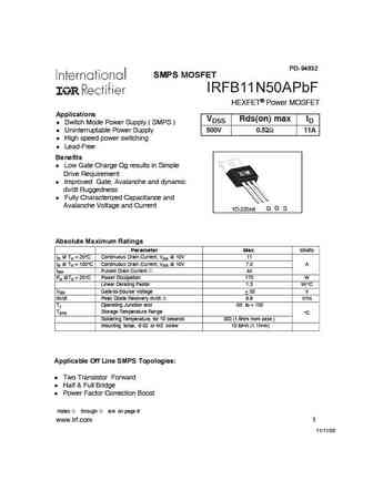
irfb11n50a.pdf
PD- 94832 SMPS MOSFET IRFB11N50APbF HEXFET Power MOSFET Applications VDSS Rds(on) max ID l Switch Mode Power Supply ( SMPS ) l Uninterruptable Power Supply 500V 0.52 11A l High speed power switching l Lead-Free Benefits l Low Gate Charge Qg results in Simple Drive Requirement l Improved Gate, Avalanche and dynamic dv/dt Ruggedness l Fully Characterized Capacitance and Avala
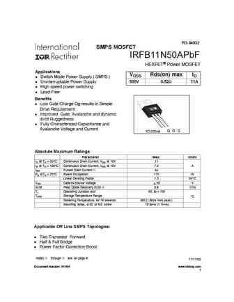
irfb11n50apbf.pdf
PD- 94832 SMPS MOSFET IRFB11N50APbF HEXFET Power MOSFET Applications VDSS Rds(on) max ID l Switch Mode Power Supply ( SMPS ) l Uninterruptable Power Supply 500V 0.52 11A l High speed power switching l Lead-Free Benefits l Low Gate Charge Qg results in Simple Drive Requirement l Improved Gate, Avalanche and dynamic dv/dt Ruggedness l Fully Characterized Capacitance and Avala
irfp31n50lpbf.pdf
PD - 95051 SMPS MOSFET IRFP31N50LPbF AppIications HEXFET Power MOSFET Trr typ. VDSS RDS(on) typ. ID 500V 0.15 170ns 31A Features and Benefits
irfsl11n50.pdf
PD- 91847B IRFSL11N50A HEXFET Power MOSFET Dynamic dv/dt Rating D Repetitive Avalanche Rated VDSS = 500V Fast Switching Ease of Paraleling RDS(on) = 0.55 Simple Drive Requirements G ID = 11A S Description Third Generation HEXFET Power MOSFETs from International Rectifier provide the designer with the best combination of fast switching, ruggedized device design, low
phx1n50e 1.pdf
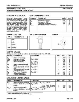
Philips Semiconductors Objective Specification PowerMOS transistor PHX1N50E Isolated version fo PHP1N50E GENERAL DESCRIPTION QUICK REFERENCE DATA N-channel enhancement mode SYMBOL PARAMETER MAX. UNIT field-effect power transistor in a full pack, plastic envelope featuring high VDS Drain-source voltage 500 V avalanche energy capability, stable ID Drain current (DC) 1.4 A blocking volt
php1n50e 1.pdf
Philips Semiconductors Objective Specification PowerMOS transistor PHP1N50E GENERAL DESCRIPTION QUICK REFERENCE DATA N-channel enhancement mode SYMBOL PARAMETER MAX. UNIT field-effect power transistor in a plastic envelope featuring high VDS Drain-source voltage 500 V avalanche energy capability, stable ID Drain current (DC) 2 A blocking voltage, fast switching and Ptot Total power dis
php11n50e phb11n50e phw11n50e.pdf
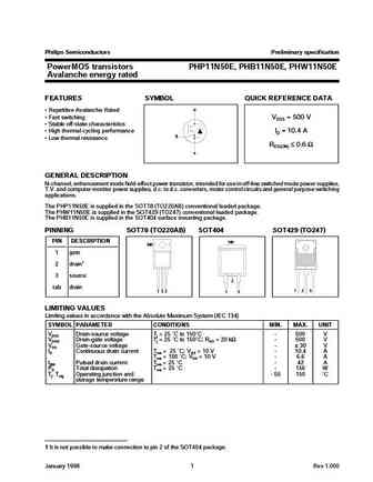
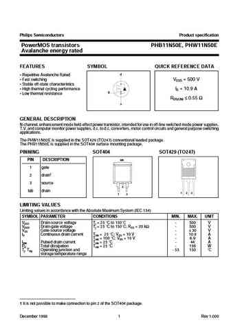
Philips Semiconductors Preliminary specification PowerMOS transistors PHP11N50E, PHB11N50E, PHW11N50E Avalanche energy rated FEATURES SYMBOL QUICK REFERENCE DATA d Repetitive Avalanche Rated Fast switching VDSS = 500 V Stable off-state characteristics High thermal cycling performance ID = 10.4 A g Low thermal resistance RDS(ON) 0.6 s GENERAL DESCRIPTI
phb11n50e phw11n50e 1.pdf
Philips Semiconductors Product specification PowerMOS transistors PHB11N50E, PHW11N50E Avalanche energy rated FEATURES SYMBOL QUICK REFERENCE DATA d Repetitive Avalanche Rated Fast switching VDSS = 500 V Stable off-state characteristics High thermal cycling performance ID = 10.9 A g Low thermal resistance RDS(ON) 0.55 s GENERAL DESCRIPTION N-channel,
std11n50m2 stf11n50m2 stf11n50m2.pdf
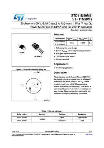
STD11N50M2, STF11N50M2 N-channel 500 V, 0.45 typ,8 A, MDmesh II Plus low Qg Power MOSFETs in DPAK and TO-220FP packages Datasheet - preliminary data Features Order codes VDS @ TJmax RDS(on) max ID STD11N50M2 550 V 0.53 8 A STF11N50M2 TAB Extremely low gate charge 3 1 Lower RDS(on) x area vs previous generation 3 DPAK 2 Low gate input resistance 1
std11n50m2 stf11n50m2.pdf
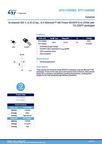
STD11N50M2, STF11N50M2 Datasheet N-channel 500 V, 0.45 typ., 8 A MDmesh M2 Power MOSFETs in DPAK and TO-220FP packages Features VDS @ TJmax RDS(on)max. ID Order code Package TAB STD11N50M2 DPAK 3 550 V 0.53 8 A 2 STF11N50M2 TO-220FP 1 3 2 1 Extremely low gate charge DPAK TO-220FP Excellent output capacitance (COSS) profile 100% avalanche tested Zen
fqnl1n50b.pdf
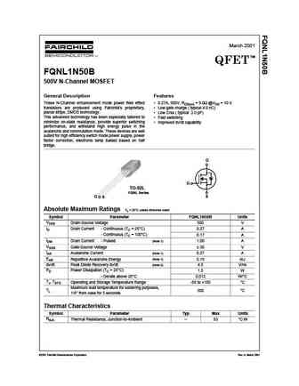
March 2001 TM QFET FQNL1N50B 500V N-Channel MOSFET General Description Features These N-Channel enhancement mode power field effect 0.27A, 500V, RDS(on) = 9.0 @VGS = 10 V transistors are produced using Fairchild s proprietary, Low gate charge ( typical 4.0 nC) planar stripe, DMOS technology. Low Crss ( typical 3.0 pF) This advanced technology has been especially tailo
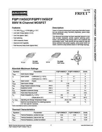
fqp11n50cf fqp11n50cf fqpf11n50cf.pdf
July 2005 TM FRFET FQP11N50CF/FQPF11N50CF 500V N-Channel MOSFET Features Description 11A, 500V, RDS(on) = 0.55 @VGS = 10 V These N-Channel enhancement mode power field effect transis- tors are produced using Fairchild s proprietary, planar stripe, Low Gate Charge (typical 43 nC) DMOS technology. Low Crss (typical 20pF) This advanced technology has been especially tai
fqn1n50cbu fqn1n50cta.pdf
January 2006 QFET FQN1N50C 500V N-Channel MOSFET Features Description 0.38 A, 500 V, RDS(on) = 6.0 @ VGS = 10 V These N-Channel enhancement mode power field effect transistors are produced using Fairchild s proprietary, planar Low gate charge ( typical 4.9 nC ) stripe, DMOS technology. This advanced technology has been especially tailored to Low Crss ( typica
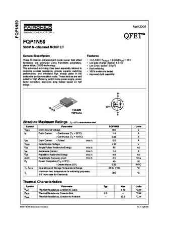
fqp1n50.pdf
April 2000 TM QFET QFET QFET QFET 500V N-ChanneI MOSFET GeneraI Description Features These N-Channel enhancement mode power field effect 1.4A, 500V, RDS(on) = 9.0 @VGS = 10 V transistors are produced using Fairchild s proprietary, Low gate charge ( typical 4.0 nC) planar stripe, DMOS technology. Low Crss ( typical 3.0 pF) This advanced technology has been
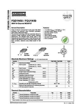
fqd1n50tf fqd1n50tm fqu1n50tu.pdf
January 2009 QFET FQD1N50 / FQU1N50 500V N-ChanneI MOSFET GeneraI Description Features These N-Channel enhancement mode power field effect 1.1A, 500V, RDS(on) = 9.0 @VGS = 10 V transistors are produced using Fairchild s proprietary, Low gate charge ( typical 4.0 nC) planar stripe, DMOS technology. Low Crss ( typical 3.0 pF) This advanced technology has been especia
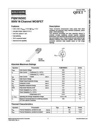
fqn1n50c.pdf
January 2006 QFET FQN1N50C 500V N-Channel MOSFET Features Description 0.38 A, 500 V, RDS(on) = 6.0 @ VGS = 10 V These N-Channel enhancement mode power field effect transistors are produced using Fairchild s proprietary, planar Low gate charge ( typical 4.9 nC ) stripe, DMOS technology. This advanced technology has been especially tailored to Low Crss ( typica
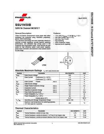
ssu1n50b.pdf
April 2014 SSU1N50B 520V N-Channel MOSFET General Description Features These N-Channel enhancement mode power field effect 1.3A, 520V, RDS(on) = 5.3 @ VGS = 10 V transistors are produced using Fairchild s proprietary, Low Gate Charge (Typ. 8.3 nC) planar, DMOS technology. Low Crss (Typ. 5.5 pF) This advanced technology has been especially tailored to Fast Switching
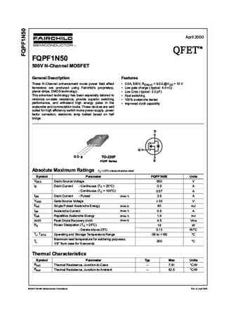
fqpf1n50.pdf
April 2000 TM QFET QFET QFET QFET 500V N-ChanneI MOSFET GeneraI Description Features These N-Channel enhancement mode power field effect 0.9A, 500V, RDS(on) = 9.0 @VGS = 10 V transistors are produced using Fairchild s proprietary, Low gate charge ( typical 4.0 nC) planar stripe, DMOS technology. Low Crss ( typical 3.0 pF) This advanced technology has bee
fqnl1n50bbu fqnl1n50bta.pdf
March 2001 TM QFET FQNL1N50B 500V N-Channel MOSFET General Description Features These N-Channel enhancement mode power field effect 0.27A, 500V, RDS(on) = 9.0 @VGS = 10 V transistors are produced using Fairchild s proprietary, Low gate charge ( typical 4.0 nC) planar stripe, DMOS technology. Low Crss ( typical 3.0 pF) This advanced technology has been especially tailo
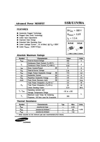
ssr1n50a.pdf
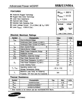
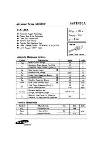
Advanced Power MOSFET FEATURES BVDSS = 500 V Avalanche Rugged Technology RDS(on) = 5.5 Rugged Gate Oxide Technology Lower Input Capacitance ID = 1.3 A Improved Gate Charge Extended Safe Operating Area Lower Leakage Current 10 A (Max.) @ VDS = 500V Lower RDS(ON) 4.046 (Typ.) 2 1 1 2 3 3 1. Gate 2. Drain 3. Source Absolute Maximum Ratings Symbol Char
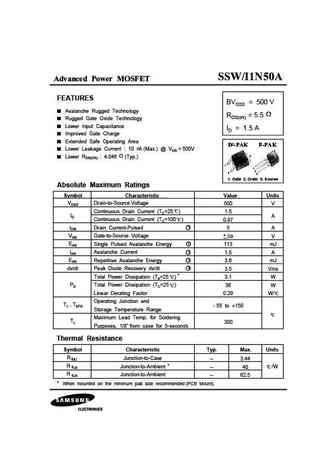
ssw1n50a.pdf
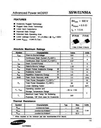
Advanced Power MOSFET FEATURES BVDSS = 500 V Avalanche Rugged Technology RDS(on) = 5.5 Rugged Gate Oxide Technology Lower Input Capacitance ID = 1.5 A Improved Gate Charge Extended Safe Operating Area Lower Leakage Current 10 A (Max.) @ VDS = 500V 2 Lower RDS(ON) 4.046 (Typ.) 1 1 2 3 3 1. Gate 2. Drain 3. Source Absolute Maximum Ratings Symbol Ch
ssp1n50a.pdf
Advanced Power MOSFET FEATURES BVDSS = 500 V Avalanche Rugged Technology RDS(on) = 5.5 Rugged Gate Oxide Technology Lower Input Capacitance ID = 1.5 A Improved Gate Charge Extended Safe Operating Area Lower Leakage Current 10 A (Max.) @ VDS = 500V Lower RDS(ON) 4.046 (Typ.) 1 2 3 1.Gate 2. Drain 3. Source Absolute Maximum Ratings Symbol Characteristic Val
irfp31n50l sihfp31n50l.pdf
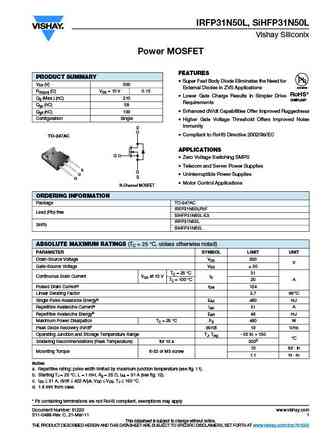
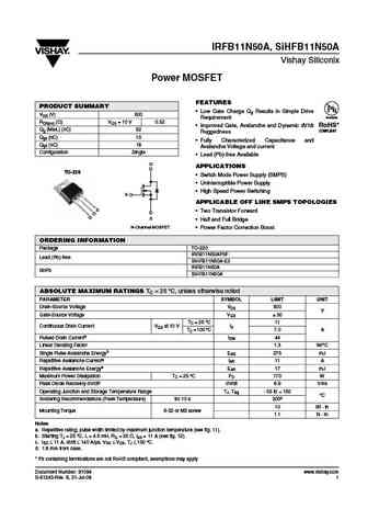
IRFP31N50L, SiHFP31N50L Vishay Siliconix Power MOSFET FEATURES PRODUCT SUMMARY Super Fast Body Diode Eliminates the Need for VDS (V) 500 External Diodes in ZVS Applications Available RDS(on) ( )VGS = 10 V 0.15 RoHS* Lower Gate Charge Results in Simpler Drive Qg (Max.) (nC) 210 COMPLIANT Requirements Qgs (nC) 58 Enhanced dV/dt Capabilities Offer Improved Ruggedness
irfsl11n50a sihfsl11n50a.pdf
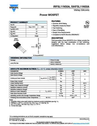
IRFSL11N50A, SiHFSL11N50A Vishay Siliconix Power MOSFET FEATURES PRODUCT SUMMARY Dynamic dV/dt Rating VDS (V) 500 Repetitive Avalanche Rated RDS(on) ( )VGS = 10 V 0.55 Fast Switching Qg (Max.) (nC) 51 Ease of Paralleling Qgs (nC) 12 Simple Drive Requirements Qgd (nC) 23 Compliant to RoHS Directive 2002/95/EC Configuration Single DESCRIPTION D I2PAK
irfsl11n50apbf sihfsl11n50a.pdf
IRFSL11N50A, SiHFSL11N50A Vishay Siliconix Power MOSFET FEATURES PRODUCT SUMMARY Dynamic dV/dt Rating VDS (V) 500 Repetitive Avalanche Rated RDS(on) ( )VGS = 10 V 0.55 Fast Switching Qg (Max.) (nC) 51 Ease of Paralleling Qgs (nC) 12 Simple Drive Requirements Qgd (nC) 23 Compliant to RoHS Directive 2002/95/EC Configuration Single DESCRIPTION D I2PAK
irfb11n50a sihfb11n50a.pdf
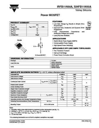
IRFB11N50A, SiHFB11N50A Vishay Siliconix Power MOSFET FEATURES PRODUCT SUMMARY Low Gate Charge Qg Results in Simple Drive VDS (V) 500 Available Requirement RDS(on) ( )VGS = 10 V 0.52 Improved Gate, Avalanche and Dynamic dV/dt RoHS* Qg (Max.) (nC) 52 COMPLIANT Ruggedness Qgs (nC) 13 Fully Characterized Capacitance and Qgd (nC) 18 Avalanche Voltage and current Confi
irfb11n50apbf.pdf
IRFB11N50A, SiHFB11N50A Vishay Siliconix Power MOSFET FEATURES PRODUCT SUMMARY Low Gate Charge Qg Results in Simple Drive VDS (V) 500 Available Requirement RDS(on) ( )VGS = 10 V 0.52 Improved Gate, Avalanche and Dynamic dV/dt RoHS* Qg (Max.) (nC) 52 COMPLIANT Ruggedness Qgs (nC) 13 Fully Characterized Capacitance and Qgd (nC) 18 Avalanche Voltage and current Confi
irfp31n50l irfp31n50lpbf sihfp31n50l.pdf
IRFP31N50L, SiHFP31N50L Vishay Siliconix Power MOSFET FEATURES PRODUCT SUMMARY Super Fast Body Diode Eliminates the Need for VDS (V) 500 External Diodes in ZVS Applications Available RDS(on) ( )VGS = 10 V 0.15 RoHS* Lower Gate Charge Results in Simpler Drive Qg (Max.) (nC) 210 COMPLIANT Requirements Qgs (nC) 58 Enhanced dV/dt Capabilities Offer Improved Ruggedness
irfs11n50apbf sihfs11n50a.pdf
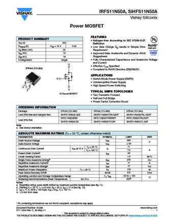
IRFS11N50A, SiHFS11N50A Vishay Siliconix Power MOSFET FEATURES PRODUCT SUMMARY Halogen-free According to IEC 61249-2-21 VDS (V) 500 Definition RDS(on) ( )VGS = 10 V 0.52 Low Gate Charge Qg results in Simple Drive Qg (Max.) (nC) 52 Requirement Qgs (nC) 13 Improved Gate, Avalanche and Dynamic dV/dt Qgd (nC) 18 Ruggedness Fully Characterized Capacitance and Avalanc
spb21n50c3.pdf
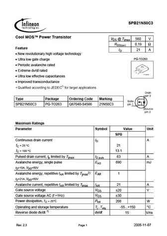
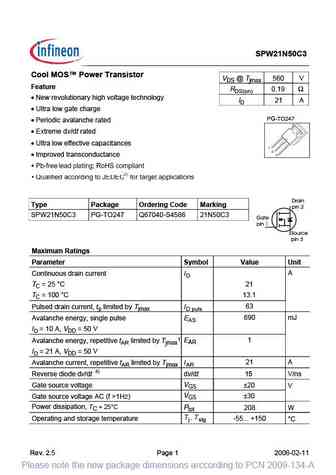
SPB21N50C3 Cool MOS Power Transistor VDS @ Tjmax 560 V RDS(on) 0.19 Feature ID 21 A New revolutionary high voltage technology PG-TO263 Ultra low gate charge Periodic avalanche rated Extreme dv/dt rated Ultra low effective capacitances Improved transconductance Type Package Ordering Code Marking SPB21N50C3 PG-TO263 Q67040-S4566 21N50C3 Maximum Rating
spp21n50c3 spi21n50c3 spa21n50c3.pdf
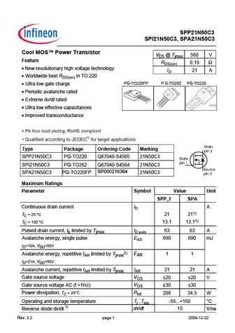
SPP21N50C3 SPI21N50C3, SPA21N50C3 Cool MOS Power Transistor VDS @ Tjmax 560 V Feature RDS(on) 0.19 New revolutionary high voltage technology ID 21 A Worldwide best RDS(on) in TO 220 PG-TO220FP P G-TO262 PG-TO220 Ultra low gate charge Periodic avalanche rated 3 Extreme dv/dt rated 2 1 Ultra low effective capacitances Improved transconductance
ixfh21n50 ixfh24n50 ixfh26n50 ixfm21n50 ixfm24n50 ixfm26n50 ixft24n50 ixft26n50.pdf
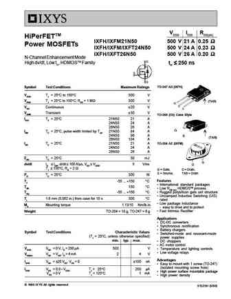
VDSS ID25 RDS(on) HiPerFETTM IXFH/IXFM21N50 500 V 21 A 0.25 Power MOSFETs IXFH/IXFM/IXFT24N50 500 V 24 A 0.23 IXFH/IXFT26N50 500 V 26 A 0.20 N-Channel Enhancement Mode High dv/dt, Low trr, HDMOSTM Family trr 250 ns TO-247 AD (IXFH) Symbol Test Conditions Maximum Ratings VDSS TJ = 25 C to
ixth21n50 ixth24n50 ixtm21n50 ixtm24n50.pdf
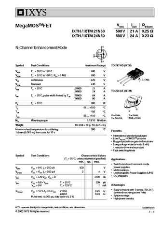
VDSS ID25 RDS(on) MegaMOSTMFET IXTH / IXTM 21N50 500 V 21 A 0.25 IXTH / IXTM 24N50 500 V 24 A 0.23 N-Channel Enhancement Mode Symbol Test Conditions Maximum Ratings TO-247 AD (IXTH) VDSS TJ = 25 C to 150 C 500 V VDGR TJ = 25 C to 150 C; RGS = 1 M 500 V D (TAB) VGS Continuous 20 V VGSM Transient 30 V ID25 TC = 25 C 21N50 21 A
ndf11n50z.pdf
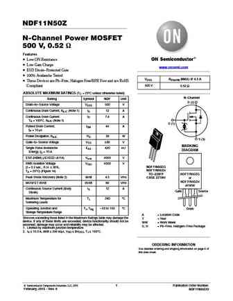
NDF11N50Z N-Channel Power MOSFET 500 V, 0.52 W Features Low ON Resistance Low Gate Charge www.onsemi.com ESD Diode-Protected Gate 100% Avalanche Tested VDSS RDS(ON) (MAX) @ 4.5 A These Devices are Pb-Free, Halogen Free/BFR Free and are RoHS 500 V Compliant 0.52 W ABSOLUTE MAXIMUM RATINGS (TC = 25 C unless otherwise noted) N-Channel Rating Symbol NDF Unit D (
1n50z.pdf
UNISONIC TECHNOLOGIES CO., LTD 1N50Z Preliminary Power MOSFET 1.3A, 500V N-CHANNEL POWER MOSFET DESCRIPTION The UTC 1N50Z is an N-channel mode power MOSFET using UTC s advanced technology to provide customers with planar stripe and DMOS technology. This technology allows a minimum on-state resistance and superior switching performance. It also can withstand high energy puls
11n50.pdf
UNISONIC TECHNOLOGIES CO., LTD 11N50 Preliminary Power MOSFET 11A, 500V N-CHANNEL POWER MOSFET 1 TO-220 DESCRIPTION The UTC 11N50 is an N-channel enhancement mode power MOSFET. It uses UTC advanced planar stripe, DMOS technology to provide customers perfect switching performance, minimal on-state 1 resistance. It also can withstand high energy pulse in the avalanche TO-22
fmv21n50es.pdf
FMV21N50ES FUJI POWER MOSFET Super FAP-E3S series N-CHANNEL SILICON POWER MOSFET Features Outline Drawings [mm] Equivalent circuit schematic Maintains both low power loss and low noise TO-220F (SLS) Lower R (on) characteristic DS More controllable switching dv/dt by gate resistance Drain(D) Smaller V ringing waveform during switching GS Narrow band of the gate threshold voltage (4.2
fmh21n50es.pdf
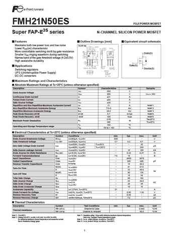
FMH21N50ES FUJI POWER MOSFET Super FAP-E3S series N-CHANNEL SILICON POWER MOSFET Features Outline Drawings [mm] Equivalent circuit schematic Maintains both low power loss and low noise TO-3P (Q) Lower R (on) characteristic DS More controllable switching dv/dt by gate resistance Drain(D) Smaller V ringing waveform during switching GS Narrow band of the gate threshold voltage (4.2 0.5
fmr21n50es.pdf
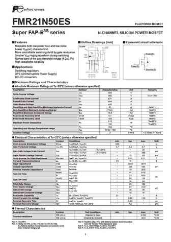
FMR21N50ES FUJI POWER MOSFET Super FAP-E3S series N-CHANNEL SILICON POWER MOSFET Features Outline Drawings [mm] Equivalent circuit schematic Maintains both low power loss and low noise TO-3PF Lower R (on) characteristic DS More controllable switching dv/dt by gate resistance Drain(D) Smaller V ringing waveform during switching GS Narrow band of the gate threshold voltage (4.2 0.5V)
mtp1n50.pdf
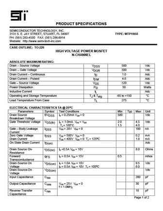
PRODUCT SPECIFICATIONS SEMICONDUCTOR TECHNOLOGY, INC. 3131 S. E. JAY STREET, STUART, FL 34997 TYPE MTP1N50 PH (561) 283-4500 FAX (561) 286-8914 Website http //www.semi-tech-inc.com CASE OUTLINE TO-220 HIGH VOLTAGE POWER MOSFET N-CHANNEL ABSOLUTE MAXIMUM RATING Drain Source Voltage VDSS 500 Vdc Drain Gate Voltage VDGR 500 Vdc Drain Current Continuous ID 1.
kf11n50p-f.pdf
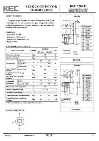
KF11N50P/F SEMICONDUCTOR N CHANNEL MOS FIELD TECHNICAL DATA EFFECT TRANSISTOR General Description KF11N50P A This planar stripe MOSFET has better characteristics, such as fast O C switching time, low on resistance, low gate charge and excellent F avalanche characteristics. It is mainly suitable for electronic ballast and E DIM MILLIMETERS G _ + switching mode power supplies. A
ap11n50i-hf.pdf
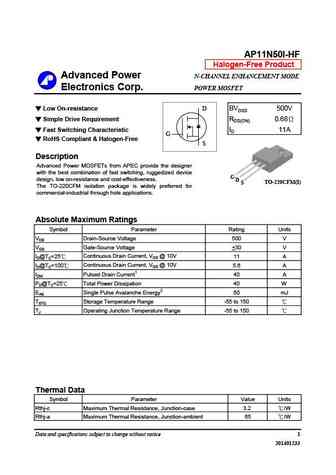
AP11N50I-HF Halogen-Free Product Advanced Power N-CHANNEL ENHANCEMENT MODE Electronics Corp. POWER MOSFET D Low On-resistance BVDSS 500V Simple Drive Requirement RDS(ON) 0.68 Fast Switching Characteristic ID 11A G RoHS Compliant & Halogen-Free S Description Advanced Power MOSFETs from APEC provide the designer with the best combination of fast switching, ruggedize
ap11n50i.pdf
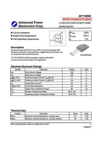
AP11N50I RoHS-compliant Product Advanced Power N-CHANNEL ENHANCEMENT MODE Electronics Corp. POWER MOSFET D Low On-resistance BVDSS 500V Simple Drive Requirement RDS(ON) 0.62 Fast Switching Characteristic ID 11A G S Description Advanced Power MOSFETs from APEC provide the designer with the best combination of fast switching, ruggedized device design, low G on-resistan
cs1n50 a1.pdf
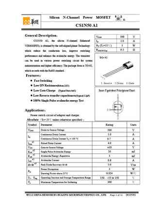
Silicon N-Channel Power MOSFET R CS1N50 A1 General Description VDSS 500 V CS1N50 A1, the silicon N-channel Enhanced ID 1.0 A PD (TC=25 ) 3 W VDMOSFETs, is obtained by the self-aligned planar Technology RDS(ON)Typ 9.5 which reduce the conduction loss, improve switching performance and enhance the avalanche energy. The transistor can be used in various power s
jfpc11n50c jffm11n50c.pdf
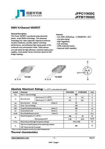
JFPC11N50C JFFM11N50C 500V N-Channel MOSFET General Description Features This Power MOSFET is produced using advanced - 11A, 500V, RDS(on)typ. = 0.46 @VGS = 10 V planar stripe DMOS technology. This advanced - Low gate charge technology has been especially tailored to minimize - High ruggedness on-state resistance, provide superior switching - Fast switching performanc
wvm21n50.pdf
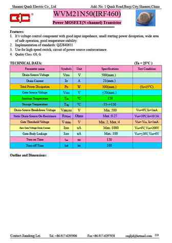
Shaanxi Qunli Electric Co., Ltd Add. No. 1 Qunli Road,Baoji City,Shaanxi,China WVM21N50(IRF460) Power MOSFET(N-channel) Transistor Features 1. It s voltage control component with good input impedance, small starting power dissipation, wide area of safe operation, good temperature stability. 2. Implementation of standards QZJ840611 3. Use for high speed switch, circuit of power s
smos21n50 smos26n50.pdf
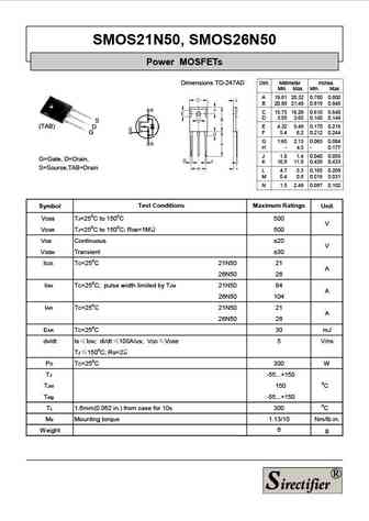
SMOS21N50, SMOS26N50 Power MOSFETs Dimensions TO-247AD Dim. Millimeter Inches Min. Max. Min. Max. A 19.81 20.32 0.780 0.800 B 20.80 21.46 0.819 0.845 C 15.75 16.26 0.610 0.640 D 3.55 3.65 0.140 0.144 S (TAB) E 4.32 5.49 0.170 0.216 D G F 5.4 6.2 0.212 0.244 G 1.65 2.13 0.065 0.084 H - 4.5 - 0.177 J 1.0 1.4 0.040 0.055 G=Gate, D=Drain, K 10.8 11.0 0.426 0.433 S=Source,TAB=Drain
msu11n50q.pdf
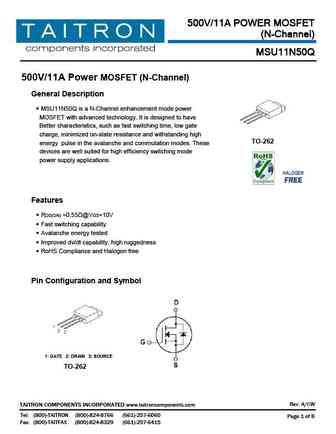
500V/11A POWER MOSFET (N-Channel) MSU11N50Q 500V/11A Power MOSFET (N-Channel) General Description MSU11N50Q is a N-Channel enhancement mode power MOSFET with advanced technology. It is designed to have Better characteristics, such as fast switching time, low gate charge, minimized on-state resistance and withstanding high TO-262 energy pulse in the avalanche and commu
tmp11n50sg tmpf11n50sg.pdf
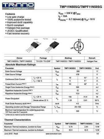
TMP11N50SG/TMPF11N50SG VDSS = 550 V @Tjmax Features ID = 10A Low gate charge RDS(ON) = 0.7 W(max) @ VGS= 10 V 100% avalanche tested Improved dv/dt capability RoHS compliant Halogen free package JEDEC Qualification Fast reverse recovery D G S Device Package Marking Remark TMP11N50SG / TMPF11N50SG TO-220 / TO-220F TMP11N50SG / TMPF11N50SG Halogen Fre
tmp11n50 tmpf11n50.pdf
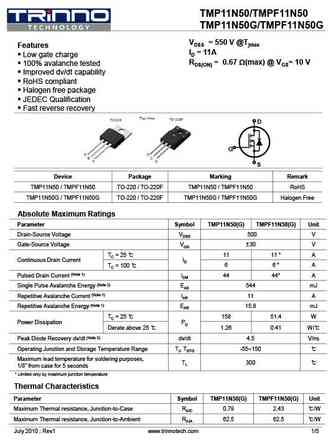
TMP11N50/TMPF11N50 TMP11N50G/TMPF11N50G VDSS = 550 V @Tjmax Features ID = 11A Low gate charge RDS(ON) = 0.67 W(max) @ VGS= 10 V 100% avalanche tested Improved dv/dt capability RoHS compliant Halogen free package JEDEC Qualification Fast reverse recovery D G S Device Package Marking Remark TMP11N50 / TMPF11N50 TO-220 / TO-220F TMP11N50 / TMPF11N50
cs1n50a1.pdf
Silicon N-Channel Power MOSFET R CS1N50 A1 General Description VDSS 500 V CS1N50 A1, the silicon N-channel Enhanced ID 1.0 A PD (TC=25 ) 3 W VDMOSFETs, is obtained by the self-aligned planar Technology RDS(ON)Typ 9.5 which reduce the conduction loss, improve switching performance and enhance the avalanche energy. The transistor can be used in various power s
cst1n50dlu cst1n50dld cst1n50dlf.pdf
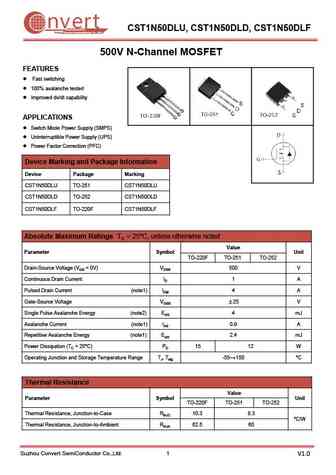
nvert CST1N50DLU, CST1N50DLD, CST1N50DLF Suzhou Convert Semiconductor Co ., Ltd. 500V N-Channel MOSFET FEATURES Fast switching 100% avalanche tested Improved dv/dt capability APPLICATIONS Switch Mode Power Supply (SMPS) Uninterruptible Power Supply (UPS) Power Factor Correction (PFC) Device Marking and Package Information Device Package Marking CST1N50DLU T
hm1n50mr.pdf
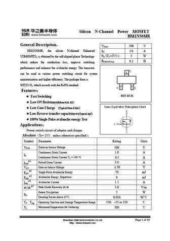
Silicon N-Channel Power MOSFET HM1N50MR General Description VDSS 500 V HM1N50MR, the silicon N-channel Enhanced ID 1.0 A PD (TC=25 ) 3 W VDMOSFETs, is obtained by the self-aligned planar Technology RDS(ON)Typ 9.2 which reduce the conduction loss, improve switching performance and enhance the avalanche energy. The transistor can be used in various power switching cir
irfp31n50l.pdf
iscN-Channel MOSFET Transistor IRFP31N50L FEATURES Low drain-source on-resistance RDS(ON) =0.18 (MAX) Enhancement mode Vth = 3.0 to 5.0V (VDS = 10 V, ID=0.25mA) 100% avalanche tested Minimum Lot-to-Lot variations for robust device performance and reliable operation DESCRITION Switching Voltage Regulators ABSOLUTE MAXIMUM RATINGS(T =25 ) a SYMBOL PARAMETER VAL
irfs11n50a.pdf
iscN-Channel MOSFET Transistor IRFS11N50A FEATURES Low drain-source on-resistance RDS(ON) =0.52 (MAX) Enhancement mode Vth = 2.0 to 4.0V (VDS = 10 V, ID=0.25mA) 100% avalanche tested Minimum Lot-to-Lot variations for robust device performance and reliable operation DESCRITION Switching Voltage Regulators ABSOLUTE MAXIMUM RATINGS(T =25 ) a SYMBOL PARAMETER VAL
spp21n50c3.pdf
isc N-Channel MOSFET Transistor SPP21N50C3 ISPP21N50C3 FEATURES Static drain-source on-resistance RDS(on) 190m Enhancement mode Fast Switching Speed 100% avalanche tested Minimum Lot-to-Lot variations for robust device performance and reliable operation DESCRITION New revolutionary high voltage technology Ultra low effective capacitance ABSOLUTE MAXIMUM
spw21n50c3.pdf
isc N-Channel MOSFET Transistor SPW21N50C3 ISPW21N50C3 FEATURES Static drain-source on-resistance RDS(on) 190m Enhancement mode 100% avalanche tested Minimum Lot-to-Lot variations for robust device performance and reliable operation DESCRITION Improved Transconductance ABSOLUTE MAXIMUM RATINGS(T =25 ) a SYMBOL PARAMETER VALUE UNIT V Drain-Source Voltage 50
Другие MOSFET... 24N50 , 26N50 , UF830 , UF830Z , UF840 , UK3568 , UF450 , UF460 , IRF9540N , 1N50Z , 2N50 , 3N50 , 3N50Z , 4N50 , 5N50 , 5N50K , 6N50 .


Список транзисторов
Обновления
MOSFET: AOTF20N40L | AOTF11N60L | AOT11N60L | AONS21303C | AOI280A60 | AOB66914L | AO3485C | AOI780A70 | AOB42S60L | AOTF950A70L | AOTF27S60L | AOTF11S60L | AONV070V65G1 | AOM065V120X2Q | AOM033V120X2 | AOK500V120X2
Popular searches
mp1620 | kta1381 | bf494 | 2sc1885 | skd502t | 2sb754 | 2sc2362 | 2sd468
