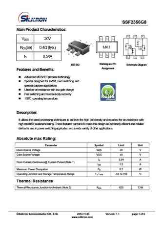
SSF2356G8. Аналоги и основные параметры
Наименование производителя: SSF2356G8
Тип транзистора: MOSFET
Полярность: N
Предельные значения
Pd ⓘ
- Максимальная рассеиваемая мощность: 0.2 W
|Vds|ⓘ - Максимально допустимое напряжение сток-исток: 20 V
|Vgs|ⓘ - Максимально допустимое напряжение затвор-исток: 8 V
|Id| ⓘ - Максимально допустимый постоянный ток стока: 0.54 A
Tj ⓘ - Максимальная температура канала: 150 °C
Электрические характеристики
Cossⓘ - Выходная емкость: 17 pf
RDSonⓘ - Сопротивление сток-исток открытого транзистора: 0.55 Ohm
Тип корпуса: SOT363
Аналог (замена) для SSF2356G8
- подборⓘ MOSFET транзистора по параметрам
SSF2356G8 даташит
9.1. Size:229K silikron
ssf2314.pdf 
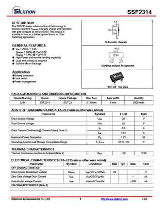
SSF2314 D DESCRIPTION The SSF2314 uses advanced trench technology to provide excellent RDS(ON), low gate charge and operation G with gate voltages as low as 0.65V. This device is suitable for use as a Battery protection or in other Switching application. S Schematic diagram GENERAL FEATURES V = 20V,I = 4.5A DS D R
9.2. Size:342K silikron
ssf2300.pdf 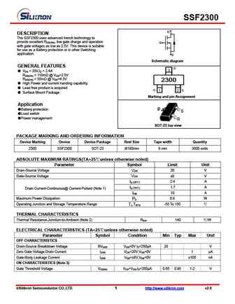
SSF2300 D DESCRIPTION The SSF2300 uses advanced trench technology to provide excellent RDS(ON), low gate charge and operation G with gate voltages as low as 2.5V. This device is suitable for use as a Battery protection or in other Switching application. S Schematic diagram GENERAL FEATURES VDS = 20V,ID = 2.4A RDS(ON)
9.3. Size:401K silikron
ssf2300a.pdf 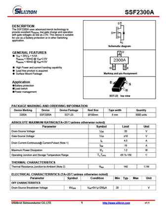
SSF2300A D DESCRIPTION The SSF2300A uses advanced trench technology to provide excellent RDS(ON), low gate charge and operation G with gate voltages as low as 2.5V. This device is suitable for use as a Battery protection or in other Switching application. S Schematic diagram GENERAL FEATURES VDS = 20V,ID = 4.5A RDS(ON)
9.4. Size:200K silikron
ssf2316e.pdf 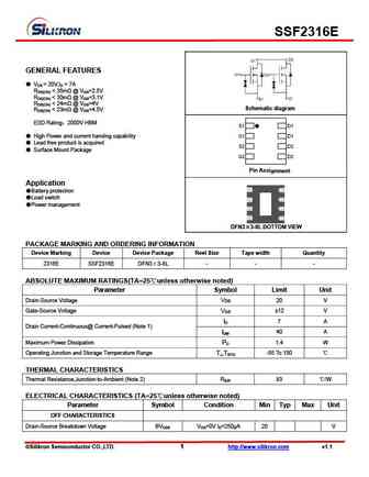
SSF2316E GENERAL FEATURES VDS = 20V,ID = 7A RDS(ON)
9.5. Size:535K silikron
ssf2341e.pdf 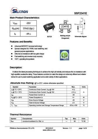
SSF2341E Main Product Characteristics VDSS -20V RDS(on) 37m (typ.) ID -4A Marking and pin SOT-23 Schematic diagram Assignme nt Features and Benefits Advanced MOSFET process technology Special designed for PWM, load switching and general purpose applications Ultra low on-resistance with low gate charge Fast switching and reverse body recovery
9.6. Size:302K silikron
ssf2306.pdf 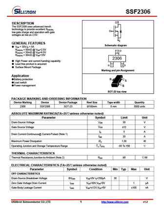
SSF2306 D DESCRIPTION The SSF2306 uses advanced trench technology to provide excellent RDS(ON), G low gate charge and operation with gate voltages as low as 2.5V. S GENERAL FEATURES Schematic diagram VDS = 30V,ID = 5A RDS(ON)
9.7. Size:282K silikron
ssf2301b.pdf 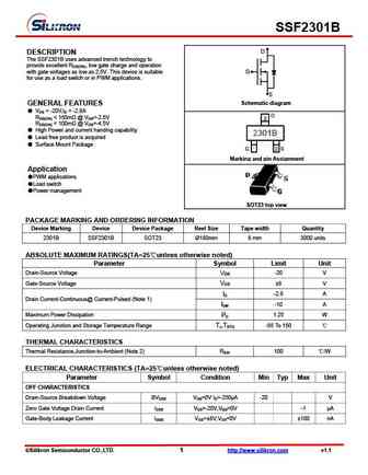
SSF2301B D DESCRIPTION The SSF2301B uses advanced trench technology to provide excellent RDS(ON), low gate charge and operation with gate voltages as low as 2.5V. This device is suitable G for use as a load switch or in PWM applications. S Schematic diagram GENERAL FEATURES VDS = -20V,ID = -2.8A RDS(ON)
9.8. Size:302K silikron
ssf2300b.pdf 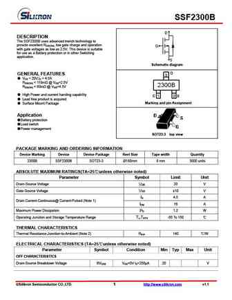
SSF2300B D DESCRIPTION The SSF2300B uses advanced trench technology to provide excellent R , low gate charge and operation DS(ON) G with gate voltages as low as 2.5V. This device is suitable for use as a Battery protection or in other Switching application. S Schematic diagram GENERAL FEATURES V = 20V,I = 4.5A DS D R
9.9. Size:317K silikron
ssf2307b.pdf 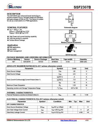
SSF2307B D DESCRIPTION The SSF2307B uses advanced trench technology to provide excellent RDS(ON), low gate charge and operation with gate voltages as low as 2.5V. This device is suitable G for use as a load switch or in PWM applications. S Schematic diagram GENERAL FEATURES VDS = -20V,ID = -3A RDS(ON)
9.10. Size:264K silikron
ssf2336.pdf 
SSF2336 D DESCRIPTION The SSF2336 uses advanced trench technology to provide excellent RDS(ON), low gate charge and operation G with gate voltages as low as 2.5V. This device is suitable for use as a Battery protection or in other Switching application. S Schematic diagram GENERAL FEATURES VDS = 20V,ID = 4.2A RDS(ON)
9.11. Size:341K silikron
ssf2318e.pdf 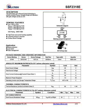
SSF2318E DESCRIPTION The SSF2318E uses advanced trench technology to provide excellent RDS(ON), low gate charge and operation with gate voltages as low as 2.5V. GENERAL FEATURES VDS = 20V,ID =6.5A Schematic diagram RDS(ON)
9.12. Size:275K silikron
ssf2301a.pdf 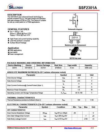
SSF2301A D DESCRIPTION The SSF2301A uses advanced trench technology to provide excellent RDS(ON), low gate charge and operation with gate voltages as low as 2.5V. This device is suitable G for use as a load switch or in PWM applications. S Schematic diagram GENERAL FEATURES VDS = -20V,ID = -4A RDS(ON)
9.13. Size:323K silikron
ssf2305.pdf 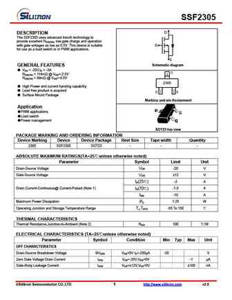
SSF2305 D DESCRIPTION The SSF2305 uses advanced trench technology to provide excellent RDS(ON), low gate charge and operation with gate voltages as low as 0.5V. This device is suitable G for use as a load switch or in PWM applications. S Schematic diagram GENERAL FEATURES VDS = -20V,ID = -3A RDS(ON)
9.14. Size:566K silikron
ssf2301.pdf 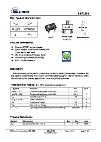
SSF2301 Main Product Characteristics D VDSS -20V G RDS(on) 60m (typ.) S ID -3A Marking and pin SOT-23 Schematic diagram Assignme nt Features and Benefits Advanced MOSFET process technology Special designed for PWM, load switching and general purpose applications Ultra low on-resistance with low gate charge Fast switching and reverse body re
9.15. Size:387K silikron
ssf2302.pdf 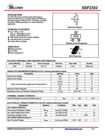
SSF2302 D DESCRIPTION The SSF2302 uses advanced trench technology to provide excellent RDS(ON), low gate charge and operation G with gate voltages as low as 2.5V. This device is suitable for use as a Battery protection or in other Switching application. S Schematic diagram GENERAL FEATURES VDS = 20V,ID = 2.4A D 3 RDS(ON)
9.16. Size:281K silikron
ssf2312.pdf 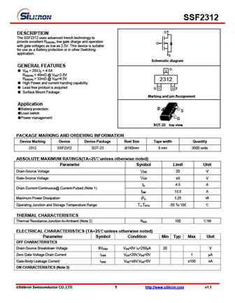
SSF2312 D DESCRIPTION The SSF2312 uses advanced trench technology to provide excellent RDS(ON), low gate charge and operation G with gate voltages as low as 2.5V. This device is suitable for use as a Battery protection or in other Switching application. S Schematic diagram GENERAL FEATURES D VDS = 20V,ID = 4.5A 3 RDS(ON)
9.17. Size:445K goodark
gdssf2300.pdf 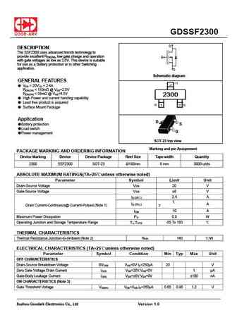
GDSSF2300 D DESCRIPTION The SSF2300 uses advanced trench technology to provide excellent RDS(ON), low gate charge and operation G with gate voltages as low as 2.5V. This device is suitable for use as a Battery protection or in other Switching application. S Schematic diagram GENERAL FEATURES VDS = 20V,ID = 2.4A RDS(ON)
9.18. Size:911K cn vbsemi
ssf2341e.pdf 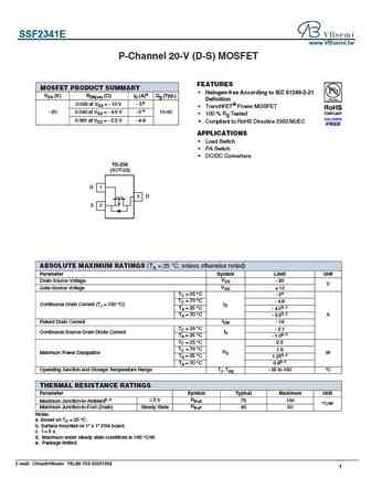
SSF2341E www.VBsemi.tw P-Channel 20-V (D-S) MOSFET FEATURES MOSFET PRODUCT SUMMARY Halogen-free According to IEC 61249-2-21 VDS (V) RDS(on) ( )ID (A)a Qg (Typ.) Definition 0.035 at VGS = - 10 V - 5e TrenchFET Power MOSFET e - 20 0.043 at VGS = - 4.5 V - 5 10 nC 100 % Rg Tested 0.061 at VGS = - 2.5 V - 4.8 Compliant to RoHS Directive 2002/95/EC APPLICATION
Другие IGBT... SSF2306, SSF2307B, SSF2312, SSF2314, SSF2316E, SSF2318E, SSF2336, SSF2341E, AO3401, SSF2418E, SSF2418EB, SSF2429, SSF2437E, SSF2449, SSF2485, SSF2610E, SSF2616E