SSF5N60G. Аналоги и основные параметры
Наименование производителя: SSF5N60G
Тип транзистора: MOSFET
Полярность: N
Предельные значения
Pd ⓘ
- Максимальная рассеиваемая мощность: 126 W
|Vds|ⓘ - Максимально допустимое напряжение сток-исток: 600 V
|Vgs|ⓘ - Максимально допустимое напряжение затвор-исток: 30 V
|Id| ⓘ - Максимально допустимый постоянный ток стока: 5 A
Tj ⓘ - Максимальная температура канала: 150 °C
Электрические характеристики
tr ⓘ -
Время нарастания: 6.8 ns
Cossⓘ - Выходная емкость: 66.65 pf
RDSonⓘ - Сопротивление сток-исток открытого транзистора: 2.15 Ohm
Тип корпуса: IPAK
Аналог (замена) для SSF5N60G
- подборⓘ MOSFET транзистора по параметрам
SSF5N60G даташит
..1. Size:491K silikron
ssf5n60g.pdf 
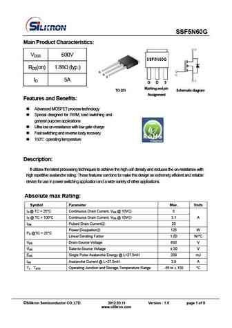
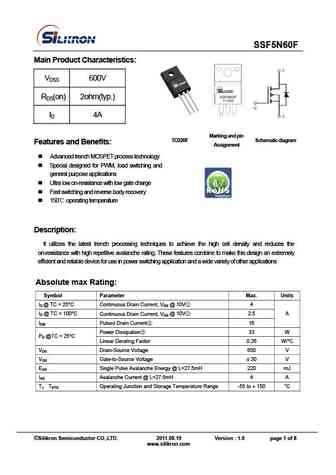
SSF5N60G Main Product Characteristics VDSS 600V RDS(on) 1.88 (typ.) ID 5A TO-251 Marking a nd p in Sche ma ti c di agr a m Assignment Features and Benefits Advanced MOSFET process technology Special designed for PWM, load switching and general purpose applications Ultra low on-resistance with low gate charge Fast switching and reverse body recovery
7.1. Size:483K silikron
ssf5n60d.pdf 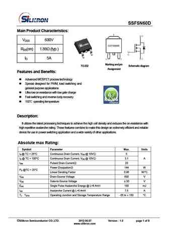
SSF5N60D Main Product Characteristics VDSS 600V RDS(on) 1.88 (typ.) ID 5A TO-252 Marking a nd p in Sche ma ti c di agr a m Assignment Features and Benefits Advanced MOSFET process technology Special designed for PWM, load switching and general purpose applications Ultra low on-resistance with low gate charge Fast switching and reverse body recovery
9.3. Size:459K silikron
ssf5ns65ug.pdf 
SSF5NS65UG Main Product Characteristics VDSS 650V RDS(on) 1.1 (typ.) ID 5A TO-251 (IPAK) Marking and p in Schematic diagram Assignment Features and Benefits High dv/dt and avalanche capabilities 100% avalanche tested Low input capacitance and gate charge Low gate input resistance Description The SSF5NS65UG series MOSFETs is a new technology,
9.4. Size:480K silikron
ssf5ns50u.pdf 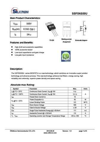
SSF5NS50U Main Product Characteristics VDSS 500V RDS(on) 0.55 (typ.) ID 5A Marking and pi n TO-220 Schematic diagram Assignment Features and Benefits High dv/dt and avalanche capabilities 100% avalanche tested Low input capacitance and gate charge Low gate input resistance Description The SSF5NS50U series MOSFETs is a new technology, which
9.5. Size:430K silikron
ssf5ns70ug.pdf 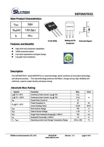
SSF5NS70UG Main Product Characteristics VDSS 700V RDS(on) 1.0 (typ.) ID 5A TO-251 (IPAK) Marking and P in Schematic Diagram Assignment Features and Benefits High dv/dt and avalanche capabilities 100% avalanche tested Low input capacitance and gate charge Low gate input resistance Description The SSF5NS70UG series MOSFETs is a new technology, whi
9.6. Size:485K silikron
ssf5ns60ud.pdf 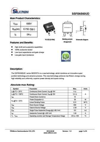
SSF5NS60UD Main Product Characteristics VDSS 600V RDS(on) 0.73 (typ.) ID 5A TO-252 (D-PAK) Marking a nd p in Sche ma ti c di agr a m Assignment Features and Benefits High dv/dt and avalanche capabilities 100% avalanche tested Low input capacitance and gate charge Low gate input resistance Description The SSF5NS60UD series MOSFETs is a new tec
9.7. Size:521K silikron
ssf5n50d.pdf 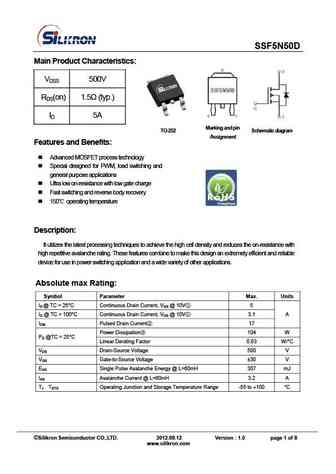
SSF5N50D Main Product Characteristics VDSS 500V RDS(on) 1.5 (typ.) ID 5A TO-252 Marking a nd p in S che ma ti c di ag r a m Assignment Features and Benefits Advanced MOSFET process technology Special designed for PWM, load switching and general purpose applications Ultra low on-resistance with low gate charge Fast switching and reverse body recovery
9.8. Size:547K silikron
ssf5ns70g-d-f.pdf 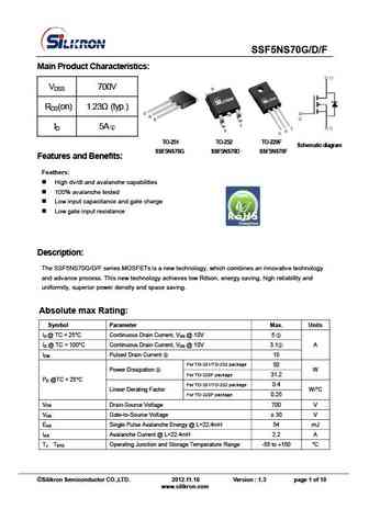
SSF5NS70G/D/F Main Product Characteristics VDSS 700V RDS(on) 1.23 (typ.) ID 5A 251 TO-252 TO- TO-220F Schematic diagram SSF5NS70G SSF5NS70D SSF5NS70F Features and Benefits Feathers High dv/dt and avalanche capabilities 100% avalanche tested Low input capacitance and gate charge Low gate input resistance Description The SSF5NS70G/D/F s
9.9. Size:477K silikron
ssf5ns65g.pdf 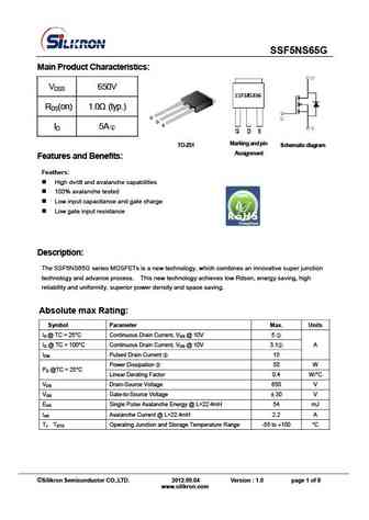
SSF5NS65G Main Product Characteristics VDSS 650V RDS(on) 1.0 (typ.) ID 5A TO-251 Marking a nd p in Sche ma ti c di agr a m Assignment Features and Benefits Feathers High dv/dt and avalanche capabilities 100% avalanche tested Low input capacitance and gate charge Low gate input resistance Description The SSF5NS65G series MOSFETs is a new te
9.10. Size:424K silikron
ssf5ns70gbp.pdf 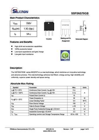
SSF5NS70GB Main Product Characteristics VDSS 700V RDS(on) 1.3 (typ.) ID 5A TO-251S Marking and Pin Schematic Diagram Assignment Features and Benefits High dv/dt and avalanche capabilities 100% avalanche tested Low input capacitance and gate charge Low gate input resistance Description The SSF5NS70GB series MOSFETs is a new technology, which com
9.11. Size:469K silikron
ssf5ns65ud.pdf 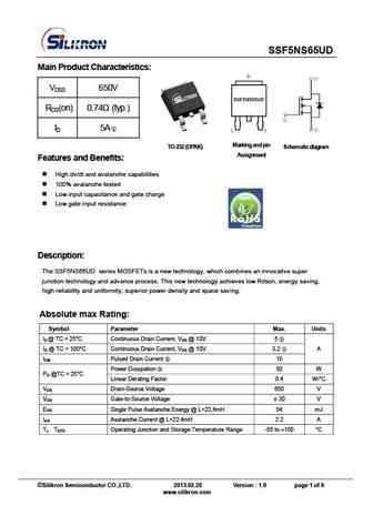
SSF5NS65UD Main Product Characteristics VDSS 650V RDS(on) 0.74 (typ.) ID 5A TO-252 (DPAK) Marking and p in Schematic diagram Assignment Features and Benefits High dv/dt and avalanche capabilities 100% avalanche tested Low input capacitance and gate charge Low gate input resistance Description The SSF5NS65UD series MOSFETs is a new technology,
9.12. Size:491K silikron
ssf5ns70uf.pdf 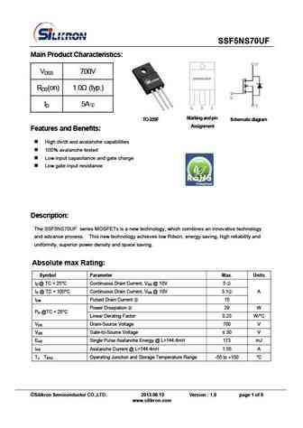
SSF5NS70UF Main Product Characteristics VDSS 700V RDS(on) 1.0 (typ.) ID 5A TO-220F Marking and pin Schematic diagram Assignment Features and Benefits High dv/dt and avalanche capabilities 100% avalanche tested Low input capacitance and gate charge Low gate input resistance Description The SSF5NS70UF series MOSFETs is a new technology, which c
9.13. Size:446K silikron
ssf5ns65uf.pdf 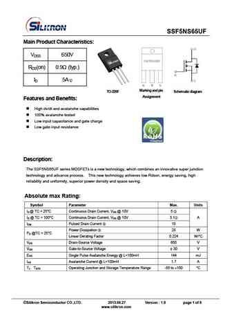
SSF5NS65UF Main Product Characteristics VDSS 650V RDS(on) 0.9 (typ.) ID 5A TO-220F Marking and p in Schematic diagram Assignment Features and Benefits High dv/dt and avalanche capabilities 100% avalanche tested Low input capacitance and gate charge Low gate input resistance Description The SSF5NS65UF series MOSFETs is a new technology, which
Другие IGBT... SSF4NS60D, SSF53A0E, SSF5506, SSF5508A, SSF5508U, SSF5N50D, SSF5N60D, SSF5N60F, IRLB4132, SSF5NS50U, SSF5NS60UD, SSF5NS65G, SSF5NS65UD, SSF5NS65UF, SSF5NS65UG, SSF5NS70G, SSF5NS70D