20P10. Аналоги и основные параметры
Наименование производителя: 20P10
Тип транзистора: MOSFET
Полярность: P
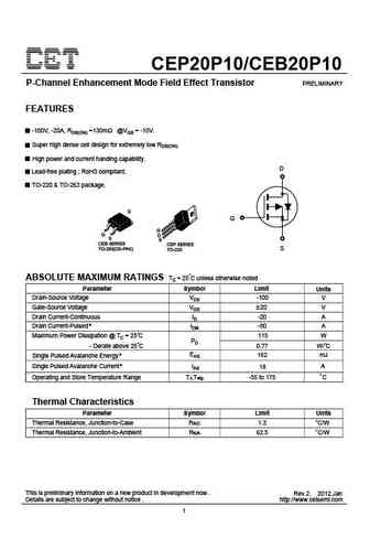
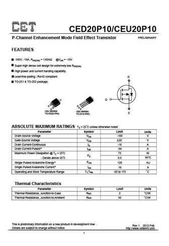
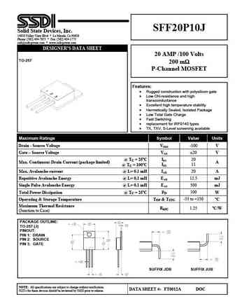
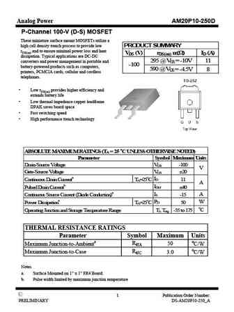
Предельные значения
Pd ⓘ - Максимальная рассеиваемая мощность: 85 W
|Vds|ⓘ - Максимально допустимое напряжение сток-исток: 100 V
|Vgs|ⓘ - Максимально допустимое напряжение затвор-исток: 20 V
|Id| ⓘ - Максимально допустимый постоянный ток стока: 20 A
Tj ⓘ - Максимальная температура канала: 150 °C
Электрические характеристики
tr ⓘ - Время нарастания: 73 ns
Cossⓘ - Выходная емкость: 590 pf
RDSonⓘ - Сопротивление сток-исток открытого транзистора: 0.1 Ohm
Тип корпуса: TO220 TO251 TO252
Аналог (замена) для 20P10
- подборⓘ MOSFET транзистора по параметрам
20P10 даташит
20p10 to220.pdf
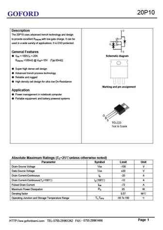
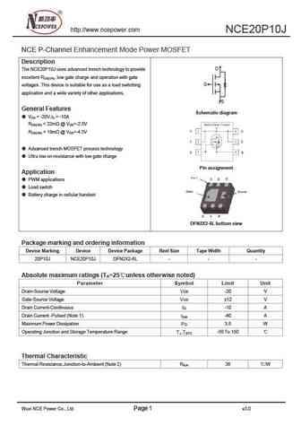
20P10 GOFORD Description The 20P10 uses advanced trench technology and design to provide excellent RDS(ON) with low gate charge. It can be used in a wide variety of applications. It is ESD protected. General Features VDS =-100V,ID =-20A Schematic diagram RDS(ON)
20p10 to251 to252.pdf
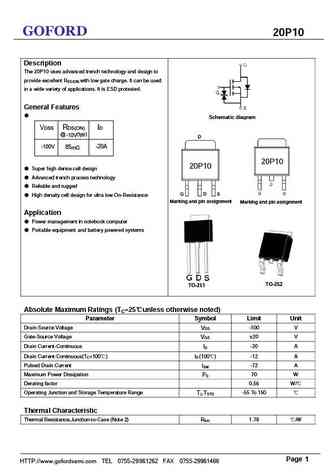
GOFORD 20P10 Description The 20P10 uses advanced trench technology and design to provide excellent R with low gate charge. It can be used DS(ON) in a wide variety of applications. It is ESD protested. General Features Schematic diagram VDSS RDS(ON) ID @ (typ) -10V -100V 85m -20A 20P10 20P10 Super high dense cell design Advanced trench process technology
mcu20p10.pdf
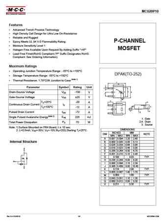
MCU20P10 Features Advanced Trench Process Technology High Density Cell Design for Ultra Low On-Resistance Reliable and Rugged Epoxy Meets UL 94 V-0 Flammability Rating P-CHANNEL Moisture Sensitivity Level 1 MOSFET Halogen Free Available Upon Request By Adding Suffix "-HF" Lead Free Finish/RoHS Compliant ("P" Suffix Designates RoHS Compliant. See Ordering In
Другие MOSFET... G15P04 , G1815 , G1816 , G1825 , 15P03 , 16N10 , 18N10 , 2002A , SI2302 , 21N06 , 22N10 , 2301H , 2301L , 25P06 , 25P10 , 25P10G , 28N10 .
🌐 : EN ES РУ

Список транзисторов
Обновления
MOSFET: ASB80R750E | ASB70R380E | ASB65R300E | ASB65R220E | ASB65R120EFD | ASB60R150E | ASA80R900E | ASA80R750E | ASA80R290E | ASA70R950E | ASA70R600E | ASA70R380E | ASA70R240E | ASA65R850E | ASA65R550E | ASA65R350E
Popular searches
c5242 reemplazo | d667 transistor datasheet | hy1d datasheet | mp20a transistor | mrf450 | oc70 transistor | p0603bd mosfet | p157r5nt