20P10 Datasheet. Specs and Replacement
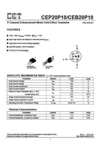
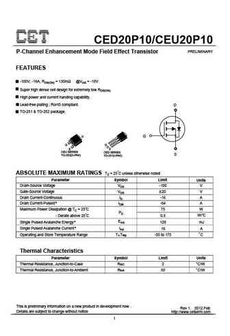
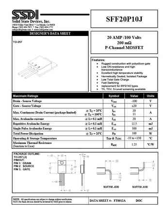
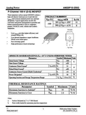
Type Designator: 20P10 📄📄
Type of Transistor: MOSFET
Type of Control Channel: P-Channel
Absolute Maximum Ratings
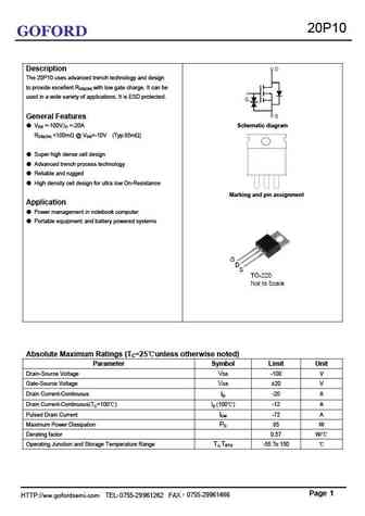
Pd ⓘ - Maximum Power Dissipation: 85 W
|Vds|ⓘ - Maximum Drain-Source Voltage: 100 V
|Vgs|ⓘ - Maximum Gate-Source Voltage: 20 V
|Id| ⓘ - Maximum Drain Current: 20 A
Tj ⓘ - Maximum Junction Temperature: 150 °C
Electrical Characteristics
tr ⓘ - Rise Time: 73 nS
Cossⓘ - Output Capacitance: 590 pF
📄📄 Copy
20P10 substitution
- MOSFET ⓘ Cross-Reference Search
20P10 datasheet
20p10 to220.pdf
20P10 GOFORD Description The 20P10 uses advanced trench technology and design to provide excellent RDS(ON) with low gate charge. It can be used in a wide variety of applications. It is ESD protected. General Features VDS =-100V,ID =-20A Schematic diagram RDS(ON) ... See More ⇒
20p10 to251 to252.pdf
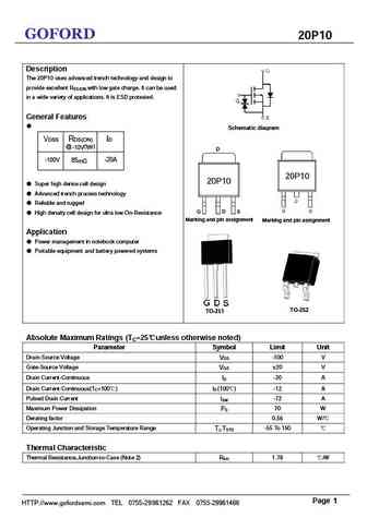
GOFORD 20P10 Description The 20P10 uses advanced trench technology and design to provide excellent R with low gate charge. It can be used DS(ON) in a wide variety of applications. It is ESD protested. General Features Schematic diagram VDSS RDS(ON) ID @ (typ) -10V -100V 85m -20A 20P10 20P10 Super high dense cell design Advanced trench process technology... See More ⇒
mcu20p10.pdf
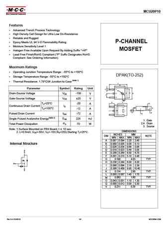
MCU20P10 Features Advanced Trench Process Technology High Density Cell Design for Ultra Low On-Resistance Reliable and Rugged Epoxy Meets UL 94 V-0 Flammability Rating P-CHANNEL Moisture Sensitivity Level 1 MOSFET Halogen Free Available Upon Request By Adding Suffix "-HF" Lead Free Finish/RoHS Compliant ("P" Suffix Designates RoHS Compliant. See Ordering In... See More ⇒
Detailed specifications: G15P04, G1815, G1816, G1825, 15P03, 16N10, 18N10, 2002A, STF13NM60N, 21N06, 22N10, 2301H, 2301L, 25P06, 25P10, 25P10G, 28N10
Keywords - 20P10 MOSFET specs
20P10 cross reference
20P10 equivalent finder
20P10 pdf lookup
20P10 substitution
20P10 replacement
Can't find your MOSFET? Learn how to find a substitute transistor by analyzing voltage, current and package compatibility
MOSFET Parameters. How They Affect Each Other
🌐 : EN ES РУ
LIST
Last Update
MOSFET: MSQ60P04D | MSQ40P07D | MSQ30P40D | MSQ30P15 | MSQ30P07D | MSQ100N03D | MSHM60P14 | MSHM40N085 | MSHM30N46 | MSH60N35D
Popular searches
c5242 reemplazo | d667 transistor datasheet | hy1d datasheet | mp20a transistor | mrf450 | oc70 transistor | p0603bd mosfet | p157r5nt
