20N15. Аналоги и основные параметры
Наименование производителя: 20N15
Тип транзистора: MOSFET
Полярность: N
Предельные значения
Pd ⓘ - Максимальная рассеиваемая мощность: 90 W
|Vds|ⓘ - Максимально допустимое напряжение сток-исток: 150 V
|Vgs|ⓘ - Максимально допустимое напряжение затвор-исток: 20 V
|Id| ⓘ - Максимально допустимый постоянный ток стока: 20 A
Tj ⓘ - Максимальная температура канала: 150 °C
Электрические характеристики
Cossⓘ - Выходная емкость: 64 pf
RDSonⓘ - Сопротивление сток-исток открытого транзистора: 0.075 Ohm
Тип корпуса: TO-252
Аналог (замена) для 20N15
- подборⓘ MOSFET транзистора по параметрам
20N15 даташит
20n15.pdf
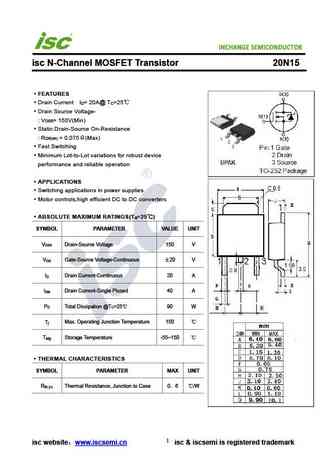
INCHANGE Semiconductor isc N-Channel MOSFET Transistor 20N15 FEATURES Drain Current I = 20A@ T =25 D C Drain Source Voltage- V = 150V(Min) DSS Static Drain-Source On-Resistance R = 0.075 (Max) DS(on) Fast Switching Minimum Lot-to-Lot variations for robust device performance and reliable operation APPLICATIONS Switching applications in power supplies Mot
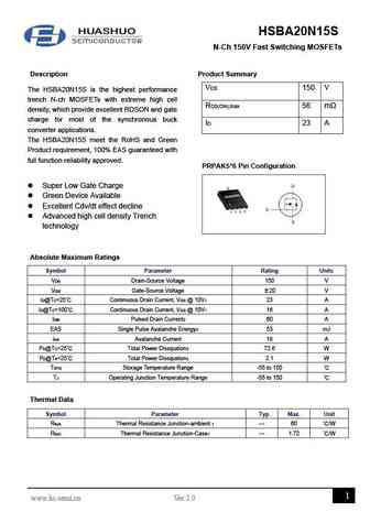
hsba20n15s.pdf
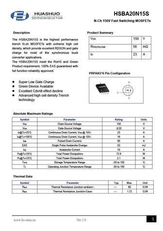
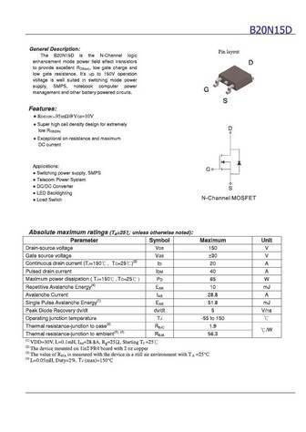
HSBA20N15S N-Ch 150V Fast Switching MOSFETs Description Product Summary VDS 150 V The HSBA20N15S is the highest performance trench N-ch MOSFETs with extreme high cell RDS(ON),max 56 m density, which provide excellent RDSON and gate charge for most of the synchronous buck ID 23 A converter applications. The HSBA20N15S meet the RoHS and Green Product requirement, 100% EA
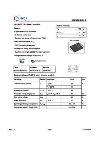
bsz520n15ns3 bsz520n15ns3g.pdf
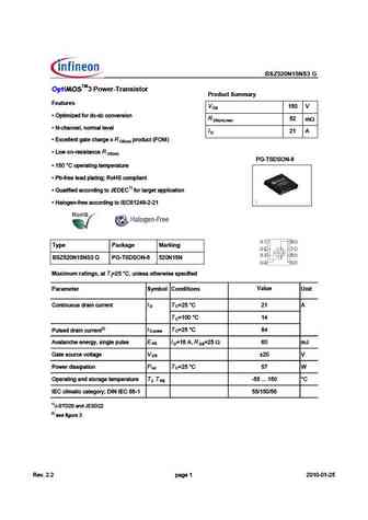
pe BSZ520N15NS3 G TM 3 Power-Transistor Product Summary Features V 1 D Q ) AD > J65 7@B 54 54 4@?F6BC @? R m D n) m x Q ( 492??6= ?@B>2= =6F6= I 1 D Q H46==6?D 82D6 492B86 H R AB@5E4D ) ' D n) Q &@G @? B6C CD2?46 R D n) G D ON Q T @A6B2D ?8 D6>A6B2DEB6 Q *3 7B66 =625 A=2D ?8 , @"- 4@>A= 2?D 1) Q + E2= 7 65 244@B5 ?8 D@ $ 7@B D2B86D 2AA= 42D @? Q "2=@86? 7B6
ixfh120n15p ixft120n15p.pdf
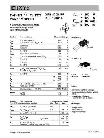
IXFH 120N15P VDSS = 150 V PolarHTTM HiPerFET IXFT 120N15P ID25 = 120 A Power MOSFET RDS(on) 16 m trr 200 ns N-Channel Enhancement Mode Avalanche Energy Rated Fast Intrinsic Diode Symbol Test Conditions Maximum Ratings TO-247 (IXFH) VDSS TJ = 25 C to 175 C 150 V VDGR TJ = 25 C to 175 C; RGS = 1 M 150 V VDSS
ixtk20n150 ixtx20n150.pdf
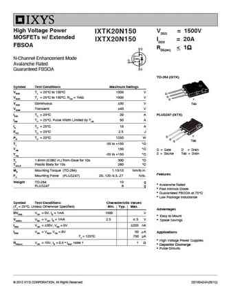
High Voltage Power VDSS = 1500V IXTK20N150 MOSFETs w/ Extended ID25 = 20A IXTX20N150 FBSOA RDS(on)
ixtq120n15p ixtt120n15p.pdf
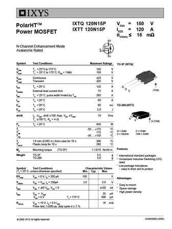
IXTQ 120N15P VDSS = 150 V PolarHTTM IXTT 120N15P ID25 = 120 A Power MOSFET RDS(on) 16 m N-Channel Enhancement Mode Avalanche Rated Symbol Test Conditions Maximum Ratings TO-3P (IXTQ) VDSS TJ = 25 C to 175 C 150 V VDGR TJ = 25 C to 175 C; RGS = 1 M 150 V VDSS Continuous 20 V VGSM Transient 30 V ID25 TC = 25 C 120 A G D
ixfx220n15p ixfk220n15p.pdf
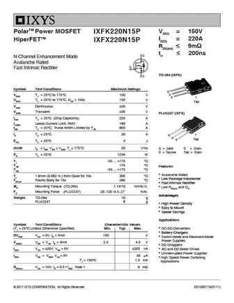
PolarTM Power MOSFET VDSS = 150V IXFK220N15P ID25 = 220A HiperFETTM IXFX220N15P RDS(on) 9m trr 200ns N-Channel Enhancement Mode Avalanche Rated Fast Intrinsic Rectifier TO-264 (IXFK) Symbol Test Conditions Maximum Ratings G VDSS TJ = 25 C to 175 C 150 V D S VDGR TJ = 25 C to 175 C, RGS = 1M 150 V Tab VGSS Conti
mcu20n15.pdf
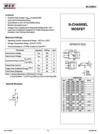
MCU20N15 Features Excellent Gate Charge x RDS(on) Product(FOM) Very Low On-Resistance RDS(on) Epoxy Meets UL 94 V-0 Flammability Rating Moisture Sensitivity Level 1 N-CHANNEL Halogen Free Available Upon Request By Adding Suffix "-HF" MOSFET Lead Free Finish/RoHS Compliant ("P" Suffix Designates RoHS Compliant. See Ordering Information) Maximum Ratings Ope
mcac20n15.pdf
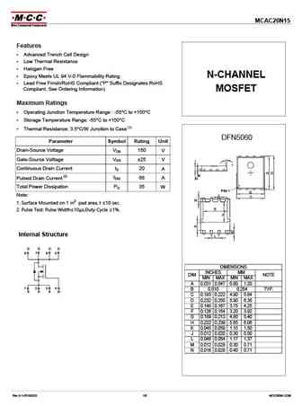
MCAC20N15 Electrical Characteristics @ 25 C (Unless Otherwise Specified) Parameter Symbol Test Conditions Min Typ Max Unit Static Characteristics V(BR)DSS VGS=0V, ID=250 A Drain-Source Breakdown Voltage 150 V IGSS VDS=0V, VGS = 25V Gate-Source Leakage Current 100 nA IDSS VDS=120V, VGS=0V Zero Gate Voltage Drain Current 1 A VGS(th) VDS=VGS, ID=250 A Gate-Threshold Voltage 2
mtp20n15e-d.pdf
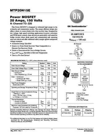
MTP20N15E Power MOSFET 20 Amps, 150 Volts N-Channel TO-220 This Power MOSFET is designed to withstand high energy in the avalanche and commutation modes. The energy efficient design also http //onsemi.com offers a drain-to-source diode with a fast recovery time. Designed for low voltage, high speed switching applications in power converters 20 AMPERES and PWM motor controls, these dev
mtp20n15eg.pdf

MTP20N15E Power MOSFET 20 Amps, 150 Volts N-Channel TO-220 This Power MOSFET is designed to withstand high energy in the avalanche and commutation modes. The energy efficient design also http //onsemi.com offers a drain-to-source diode with a fast recovery time. Designed for low voltage, high speed switching applications in power converters 20 AMPERES and PWM motor controls, these dev
ssd20n15-250d.pdf
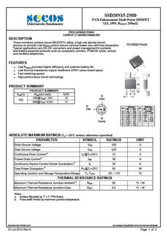
SSD20N15-250D N-Ch Enhancement Mode Power MOSFET 12A, 150V, RDS(ON) 255m Elektronische Bauelemente RoHS Compliant Product A suffix of -C specifies halogen free DESCRIPTION These miniature surface mount MOSFETs utilize a high cell density trench TO-252(D-Pack) process to provide Low RDS(on) and to ensure minimal power loss and heat dissipation. Typical applications are
ap20n15agh.pdf
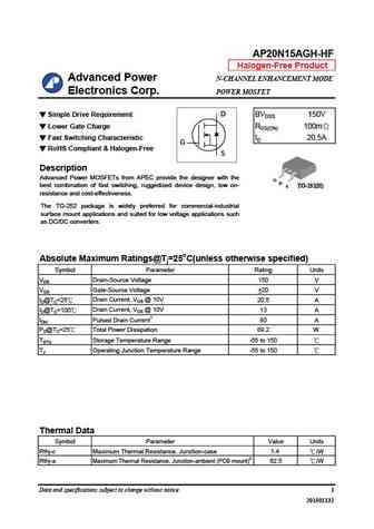
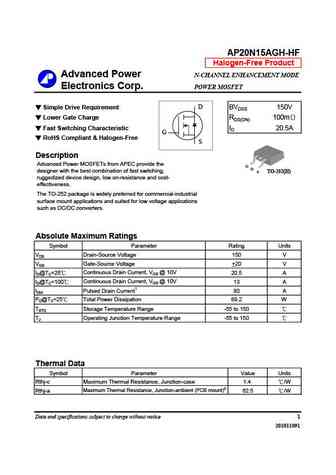
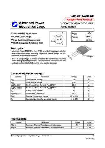
AP20N15AGH-HF Halogen-Free Product Advanced Power N-CHANNEL ENHANCEMENT MODE Electronics Corp. POWER MOSFET D Simple Drive Requirement BVDSS 150V Lower Gate Charge RDS(ON) 100m Fast Switching Characteristic ID 20.5A G RoHS Compliant & Halogen-Free S Description Advanced Power MOSFETs from APEC provide the designer with the G D best combination of fast switching,
ap20n15gh-hf.pdf
AP20N15GH-HF Halogen-Free Product Advanced Power N-CHANNEL ENHANCEMENT MODE Electronics Corp. POWER MOSFET D Simple Drive Requirement BVDSS 150V Lower Gate Charge RDS(ON) 100m Fast Switching Characteristic ID 20A G RoHS Compliant & Halogen-Free S Description G Advanced Power MOSFETs from APEC provide the D S TO-252(H) designer with the best combination of fast
ap20n15agh-hf.pdf
AP20N15AGH-HF Halogen-Free Product Advanced Power N-CHANNEL ENHANCEMENT MODE Electronics Corp. POWER MOSFET D Simple Drive Requirement BVDSS 150V Lower Gate Charge RDS(ON) 100m Fast Switching Characteristic ID 20.5A G RoHS Compliant & Halogen-Free S Description Advanced Power MOSFETs from APEC provide the G D designer with the best combination of fast switching,
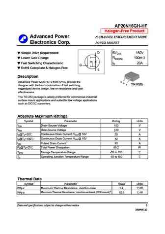
ap20n15gh.pdf
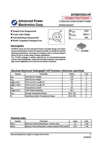
AP20N15GH-HF Halogen-Free Product Advanced Power N-CHANNEL ENHANCEMENT MODE Electronics Corp. POWER MOSFET D Simple Drive Requirement BVDSS 150V Lower Gate Charge RDS(ON) 100m Fast Switching Characteristic ID 20A G RoHS Compliant & Halogen-Free S Description AP20N15 series are from Advanced Power innovated design and silicon G D S process technology to achieve
ap20n15agi-hf.pdf
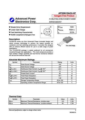
AP20N15AGI-HF Halogen-Free Product Advanced Power N-CHANNEL ENHANCEMENT MODE Electronics Corp. POWER MOSFET Simple Drive Requirement D BVDSS 150V Lower Gate Charge RDS(ON) 100m Fast Switching Characteristic ID 20.5A G RoHS Compliant & Halogen-Free S Description AP20N15A series are from Advanced Power innovated design and silicon process technology to achieve the lo
ap20n15gi.pdf
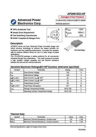
AP20N15GI-HF Halogen-Free Product Advanced Power N-CHANNEL ENHANCEMENT MODE Electronics Corp. POWER MOSFET 100% Avalanche Test D BVDSS 150V Simple Drive Requirement RDS(ON) 100m Fast Switching Characteristic ID3 20A G RoHS Compliant & Halogen-Free S Description AP20N15 series are from Advanced Power innovated design and silicon process technology to achieve the low
ap20n15agp-hf.pdf
AP20N15AGP-HF Halogen-Free Product Advanced Power N-CHANNEL ENHANCEMENT MODE Electronics Corp. POWER MOSFET Simple Drive Requirement D BVDSS 150V Lower Gate Charge RDS(ON) 100m Fast Switching Characteristic ID 20.5A G RoHS Compliant & Halogen-Free S Description Advanced Power MOSFETs from APEC provide the designer with the best combination of fast switching, rugged
ap20n15gi-hf.pdf
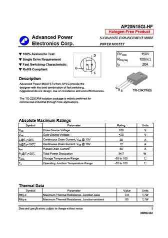
AP20N15GI-HF Halogen-Free Product Advanced Power N-CHANNEL ENHANCEMENT MODE Electronics Corp. POWER MOSFET 100% Avalanche Test BVDSS 150V D Single Drive Requirement RDS(ON) 100m Fast Switching Characteristic ID 20A G RoHS Compliant S Description Advanced Power MOSFETs from APEC provide the designer with the best combination of fast switching, G D TO-220CFM(I)
am20n15-250b.pdf
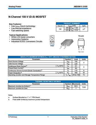
Analog Power AM20N15-250B N-Channel 150-V (D-S) MOSFET PRODUCT SUMMARY Key Features rDS(on) (m ) VDS (V) ID(A) Low r trench technology DS(on) 200 @ VGS = 10V Low thermal impedance 150 21a 225 @ VGS = 5.5V Fast switching speed Typical Applications White LED boost converters Automotive Systems Industrial DC/DC Conversion Circuits ABSOLUTE MAXIM
am20n15-250d.pdf
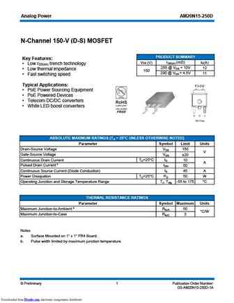
Analog Power AM20N15-250D N-Channel 150-V (D-S) MOSFET PRODUCT SUMMARY Key Features rDS(on) (m ) VDS (V) ID(A) Low r trench technology DS(on) 255 @ VGS = 10V 12 Low thermal impedance 150 290 @ VGS = 4.5V 11 Fast switching speed Typical Applications PoE Power Sourcing Equipment PoE Powered Devices Telecom DC/DC converters White LED boost
stu20n15 std20n15.pdf
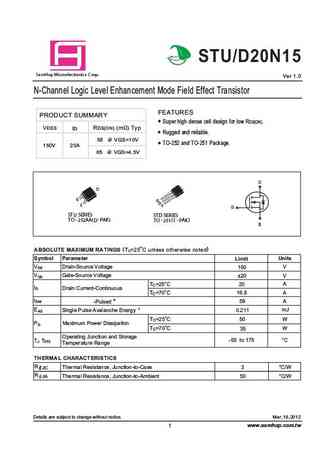
Gre r r P Pr Pr Pro STU/D20N15 a S mHop Microelectronics C orp. Ver 1.0 N-Channel Logic Level Enhancement Mode Field Effect Transistor FEATURES PRODUCT SUMMARY Super high dense cell design for low RDS(ON). RDS(ON) (m ) Typ VDSS ID Rugged and reliable. 58 @ VGS=10V TO-252 and TO-251 Package. 150V 20A 65 @ VGS=4.5V G G S S STU SERIES STD SERIES ( ) TO - 252AA D- PAK
kxp20n15.pdf
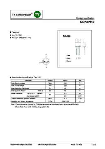
MOSFET e IC SMD Type SMD pe MOSFET DIP pe MOSFET SMD Type MOSFET DIP Type MOSFET SMDType C DIPTyType C SMDType IIC DIPTyType IIC SMDType SMDType Product specification KXP20N15 Features VDS (V) = 150V RDS(ON) 0.13 (VGS = 10V) 1 Gate 2 Drain 3 Source Absolute Maximum Ratings Ta = 25 Parameter Symbol Rating Unit Drain-Source Voltage V
ru120n15r.pdf
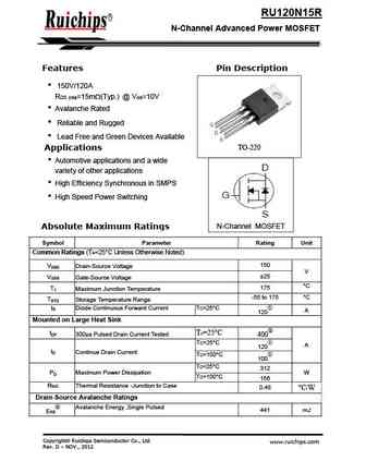
RU120N15R N-Channel Advanced Power MOSFET Features Pin Description 150V/120A RDS (ON)=15m (Typ.) @ VGS=10V Avalanche Rated Reliable and Rugged Lead Free and Green Devices Available TO-220 Applications Automotive applications and a wide variety of other applications High Efficiency Synchronous in SMPS High Speed Power Switching N-Channel MOSFET A
ru120n15q.pdf
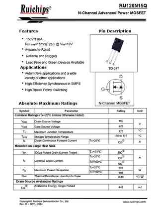
RU120N15Q N-Channel Advanced Power MOSFET Features Pin Description 150V/120A RDS (ON)=15m (Typ.) @ VGS=10V Avalanche Rated Reliable and Rugged Lead Free and Green Devices Available Applications TO-247 Automotive applications and a wide variety of other applications High Efficiency Synchronous in SMPS High Speed Power Switching N-Channel MOSFET A
me20n15 me20n15-g.pdf
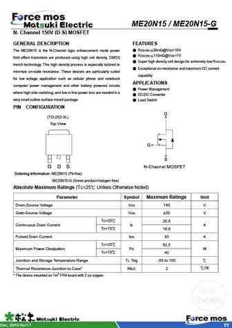
ME20N15 / ME20N15-G N- Channel 150V (D-S) MOSFET GENERAL DESCRIPTION FEATURES RDS(ON) 90m @VGS=10V The ME20N15 is the N-Channel logic enhancement mode power RDS(ON) 110m @VGS=7V field effect transistors are produced using high cell density, DMOS Super high density cell design for extremely low RDS(ON) trench technology. This high density process is especially t
me20n15f.pdf
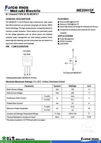
ME20N15F N- Channel 150V (D-S) MOSFET GENERAL DESCRIPTION FEATURES RDS(ON) 90m @VGS=10V The ME20N15F is the N-Channel logic enhancement mode power RDS(ON) 110m @VGS=7V field effect transistors are produced using high cell density, DMOS Super high density cell design for extremely low RDS(ON) trench technology. This high density process is especially tailored to
tgan20n150fd.pdf
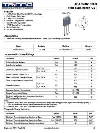
TGAN20N150FD Field Stop Trench IGBT Features TO 3PN 1500V Field Stop Trench IGBT Technology High Speed Switching Low Conduction Loss Positive Temperature Coefficient Easy Parallel Operation 175 Operating Temperature RoHS Compliant JEDEC Qualification E C G Applications Induction Heating, Inverterized Microwave Ovens, Soft Switching Appl
wmo20n15t2.pdf
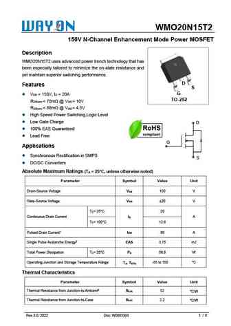
WMO20N15T2 150V N-Channel Enhancement Mode Power MOSFET Description WMO20N15T2 uses advanced power trench technology that has been especially tailored to minimize the on-state resistance and yet maintain superior switching performance. D Features S G V = 150V, I = 20A DS D TO-252 R
fir20n15lg.pdf
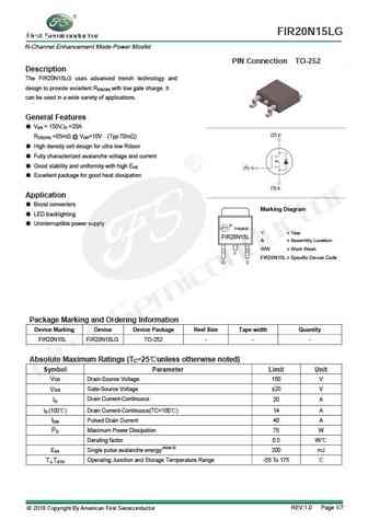
FIR20N15LG N-Channel Enhancement Mode Power Mosfet PIN Connection TO-252 Description The FIR20N15LG uses advanced trench technology and design to provide excellent RDS(ON) with low gate charge. It can be used in a wide variety of applications. General Features VDS = 150V,ID =20A RDS(ON)
damh220n150.pdf
DAMH220N150 DACO SEMICONDUCTOR CO., LTD. N-Channel Enhancement Mode MOSFET Preliminary HB-9434 Features VDSS = 150V RDS(ON)
dami220n150.pdf
DAMI220N150 DACO SEMICONDUCTOR CO., LTD. N-Channel Enhancement Mode MOSFET Preliminary SOT-227 Features S VDSS = 150V G RDS(ON)
hsu20n15a.pdf
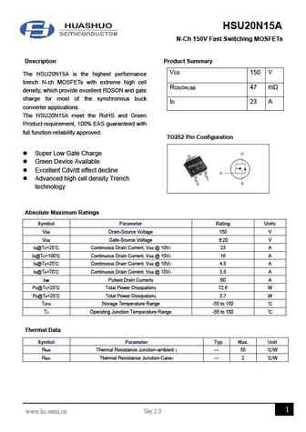
HSU20N15A N-Ch 150V Fast Switching MOSFETs Description Product Summary VDS 150 V The HSU20N15A is the highest performance trench N-ch MOSFETs with extreme high cell RDS(ON),typ 47 m density, which provide excellent RDSON and gate charge for most of the synchronous buck ID 23 A converter applications. The HSU20N15A meet the RoHS and Green Product requirement, 100% EAS g
hsba20n15s.pdf
HSBA20N15S N-Ch 150V Fast Switching MOSFETs Description Product Summary VDS 150 V The HSBA20N15S is the highest performance trench N-ch MOSFETs with extreme high cell RDS(ON),max 56 m density, which provide excellent RDSON and gate charge for most of the synchronous buck ID 23 A converter applications. The HSBA20N15S meet the RoHS and Green Product requirement, 100% EA
vbzm120n15.pdf
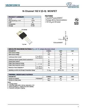
VBZM120N15 www.VBsemi.com N-Channel 150 V (D-S) MOSFET FEATURES PRODUCT SUMMARY TrenchFET power MOSFET VDS (V) 150 Package with low thermal resistance RDS(on) ( ) at VGS = 10 V 0.075 100 % Rg and UIS tested ID (A) 20 Configuration Single Package TO-220 TO-220AB D G S S N-Channel MOSFET D G Top View S ABSOLUTE MAXIMUM RATINGS (TC = 25 C, unless otherwise n
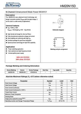
hm20n15a.pdf
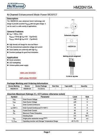
HM20N15A N-Channel Enhancement Mode Power MOSFET Description The HM20N15A uses advanced trench technology and design to provide excellent RDS(ON) with low gate charge. It can be used in a wide variety of applications. General Features VDS = 150V,ID =20A Schematic diagram RDS(ON)
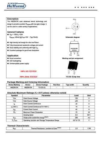
hm20n15.pdf

HM20N15 NCE N-Channel Enhancement Mode Power MOSFET Description The uses advanced trench technology and design to provide excellent RDS(ON) with low gate charge. It can be used in a wide variety of applications. General Features VDS = 150V,ID =20A RDS(ON)
hm20n15ka.pdf
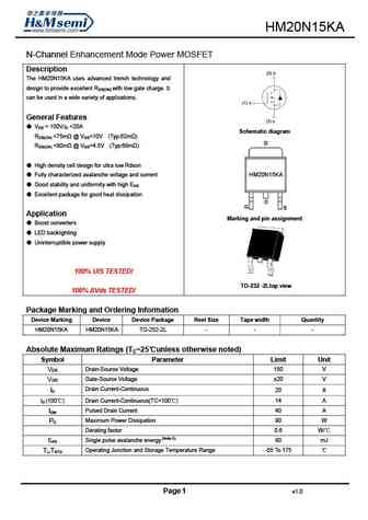
HM20N15KA N-Channel Enhancement Mode Power MOSFET Description The HM20N15KA uses advanced trench technology and design to provide excellent RDS(ON) with low gate charge. It can be used in a wide variety of applications. General Features VDS = 150V,ID =20A Schematic diagram RDS(ON)
hm20n15d.pdf
HM20N15D N-Channel Enhancement Mode Power MOSFET Description The HM20N15D uses advanced trench technology and design to provide excellent RDS(ON) with low gate charge. It can be used in a wide variety of applications. General Features VDS =150V,ID =20A RDS(ON)
hm20n15k.pdf
HM20N15K Description The HM20N15K uses advanced trench technology and design to provide excellent RDS(ON) with low gate charge. It can be used in a wide variety of applications. General Features VDS = 150V,ID =20A RDS(ON)
hms20n15k.pdf
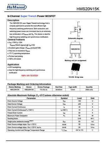
HMS20N15K N-Channel Super Trench Power MOSFET Description The HMS20N15K uses Super Trench technology that is uniquely optimized to provide the most efficient high frequency switching performance. Both conduction and switching power losses are minimized due to an extremely low combination of RDS(ON) and Qg. This device is ideal for high-frequency switching and synchronous rectific
Другие MOSFET... BLM4953A , BLM7002 , BLM7002K , BLM8205 , BLM8205A , BLM9435 , BLM9435A , BLM9926 , 2N7000 , 25N40A , 2SJ126 , 2SK1105 , 2SK1917-M , 2SK1938-01 , 2SK1939-01 , 2SK1982-01M , 2SK2020-01MR .
History: IRFBA1404P | 25N40A | FDP027N08B | 2SK1105 | FDMS3624S
History: IRFBA1404P | 25N40A | FDP027N08B | 2SK1105 | FDMS3624S
🌐 : EN ES РУ

Список транзисторов
Обновления
MOSFET: ASU70R600E | ASU65R850E | ASU65R550E | ASU65R350E | ASR65R120EFD | ASR65R046EFD | ASQ65R046EFD | ASM65R280E | ASM60R330E | ASE70R950E | ASD80R750E | ASD70R950E | ASD70R600E | ASD70R380E | ASD65R850E | ASD65R550E
Popular searches
tip142 | d882 | irf740 datasheet | ksa992 | irfb4227 | irfb4110 | tip36c | bd139 transistor