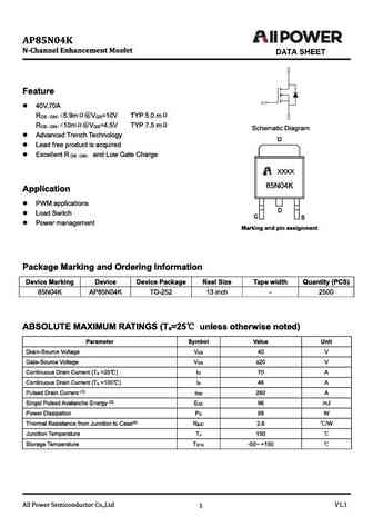
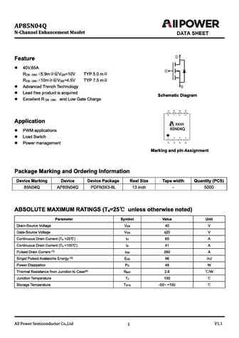
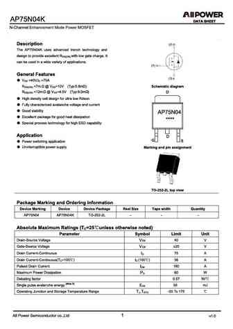
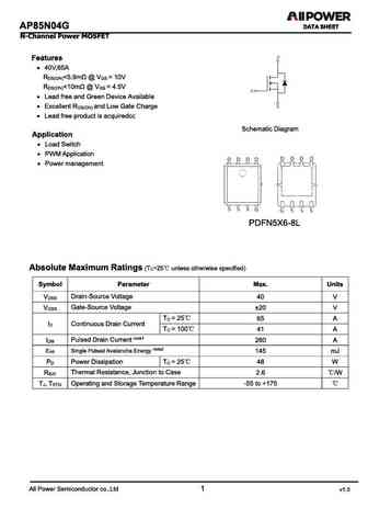
5N04. Аналоги и основные параметры
Наименование производителя: 5N04
Тип транзистора: MOSFET
Полярность: N
Предельные значения
Pd ⓘ - Максимальная рассеиваемая мощность: 0.3 W
|Vds|ⓘ - Максимально допустимое напряжение сток-исток: 40 V
|Vgs|ⓘ - Максимально допустимое напряжение затвор-исток: 20 V
|Id| ⓘ - Максимально допустимый постоянный ток стока: 5 A
Tj ⓘ - Максимальная температура канала: 150 °C
Электрические характеристики
tr ⓘ - Время нарастания: 3.5 ns
Cossⓘ - Выходная емкость: 35 pf
RDSonⓘ - Сопротивление сток-исток открытого транзистора: 0.042 Ohm
Тип корпуса: SOT23
Аналог (замена) для 5N04
- подборⓘ MOSFET транзистора по параметрам
5N04 даташит
5n04.pdf
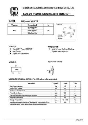
SHENZHEN HAOLIN ELECTRONICS TECHNOLOGY CO., LTD SOT-23 Plastic-Encapsulate MOSFET 5N04 N-Channel MOSFET SOT-23 ID V(BR)DSS RDS(on)MAX 3 m @10V 35 40V 50 m 5A @4.5V m @2.5V 60 1. GATE 1 2. SOURCE 2 3. DRAIN FEATURE APPLICATION TrenchFET Power MOSFET Ideal for Load Swith and Battery Low RDS(ON) Protection Applications Typical ESD Protection
hyg015n04ls1c2.pdf
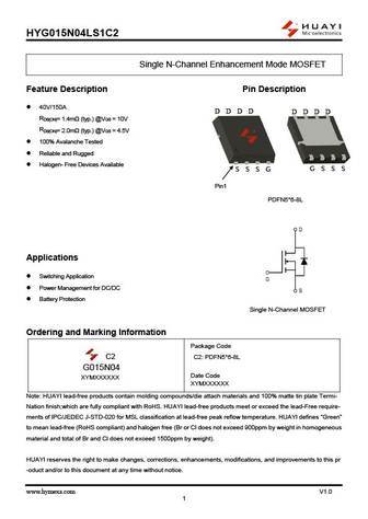
HYG015N04LS1C2 Single N-Channel Enhancement Mode MOSFET Feature Description Pin Description 40V/150A D D D D D D D D RDS(ON)= 1.4m (typ.) @VGS = 10V RDS(ON)= 2.0m (typ.) @VGS = 4.5V 100% Avalanche Tested Reliable and Rugged Halogen- Free Devices Available G S S S S S S G Pin1 PDFN5*6-8L Applications Switching Application Power Manageme
hyg025n04na1c2.pdf
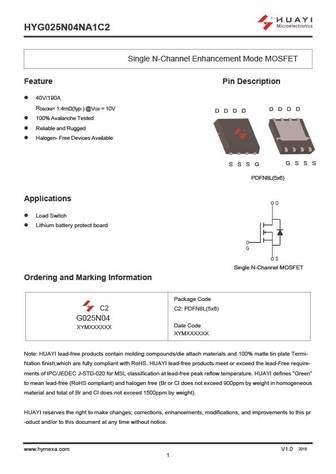
HYG025N04NA1C2 Single N-Channel Enhancement Mode MOSFET Feature Pin Description 40V/190A RDS(ON)= 1.4m (typ.) @VGS = 10V D D D D D D D D 100% Avalanche Tested Reliable and Rugged Halogen- Free Devices Available G S S S S S S G PDFN8L(5x6) Applications Load Switch Lithium battery protect board Single N-Channel MOSFET Ordering and Marking Information Pac
cjab25n04.pdf
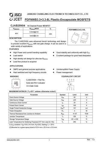
JIANGSU CHANGJING ELECTRONICS TECHNOLOGY CO., LTD PDFNWB3.3 3.3-8L Plastic-Encapsulate MOSFETS CJAB25N04 N-Channel Power MOSFET ID V(BR)DSS RDS(on)MAX PDFNWB3.3 3.3-8L 9.5m @10V 40V 25A 16m @4.5V DESCRIPTION The CJAB25N04 uses advanced trench technology and design to provide excellent RDS(ON) with low gate charge. It can be used in a wide variety of applications FEAT
std95n04 std95n04 stp95n04 stp95n04.pdf
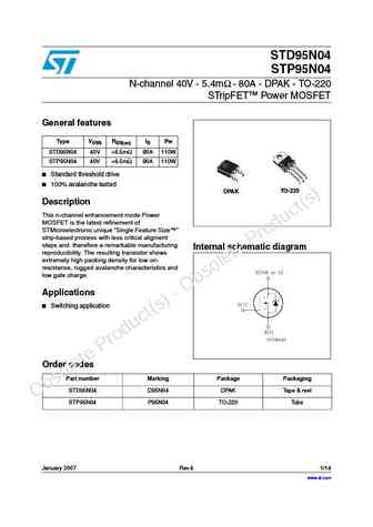
STD95N04 STP95N04 N-channel 40V - 5.4m - 80A - DPAK - TO-220 STripFET Power MOSFET General features Type VDSS RDS(on) ID Pw STD95N04 40V
np75n04yuk.pdf
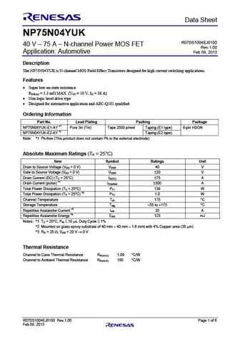
Preliminary Data Sheet NP75N04YUK R07DS1004EJ0100 40 V 75 A N-channel Power MOS FET Rev.1.00 Application Automotive Feb 08, 2013 Description The NP75N04YUK is N-channel MOS Field Effect Transistors designed for high current switching applications. Features Super low on-state resistance RDS(on) = 3.3 m MAX. (VGS = 10 V, ID = 38 A) Non logic level drive typ
np75n04yug.pdf

Preliminary Data Sheet NP75N04YUG R07DS0018EJ0100 Rev.1.00 MOS FIELD EFFECT TRANSISTOR Jul 01, 2010 Description The NP75N04YUG is N-channel MOS Field Effect Transistor designed for high current switching applications. Features Low on-state resistance RDS(on) = 4.8 m MAX. (VGS = 10 V, ID = 37.5 A) Low Ciss Ciss = 4300 pF TYP. (VDS = 25 V, VGS = 0 V) Designe
np55n04sug.pdf
To our customers, Old Company Name in Catalogs and Other Documents On April 1st, 2010, NEC Electronics Corporation merged with Renesas Technology Corporation, and Renesas Electronics Corporation took over all the business of both companies. Therefore, although the old company name remains in this document, it is a valid Renesas Electronics document. We appreciate your understanding.
np35n04yug.pdf
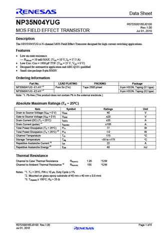
Preliminary Data Sheet NP35N04YUG R07DS0016EJ0100 Rev.1.00 MOS FIELD EFFECT TRANSISTOR Jul 01, 2010 Description The NP35N04YUG is N-channel MOS Field Effect Transistor designed for high current switching applications. Features Low on-state resistance RDS(on) = 10 m MAX. (VGS = 10 V, ID = 17.5 A) Low Ciss Ciss = 1900 pF TYP. (VDS = 25 V, VGS = 0 V) Designed
np35n04ylg.pdf
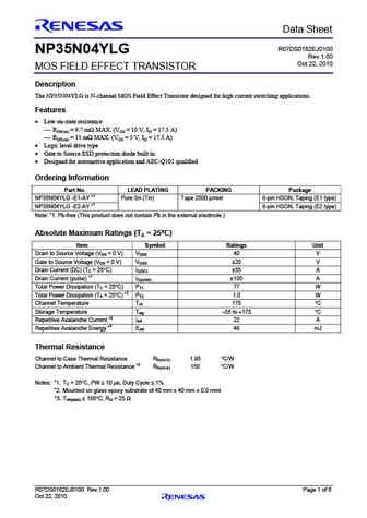
Preliminary Data Sheet R07DS0182EJ0100 NP35N04YLG Rev.1.00 Oct 22, 2010 MOS FIELD EFFECT TRANSISTOR Description The NP35N04YLG is N-channel MOS Field Effect Transistor designed for high current switching applications. Features Low on-state resistance RDS(on) = 9.7 m MAX. (VGS = 10 V, ID = 17.5 A) RDS(on) = 15 m MAX. (VGS = 5 V, ID = 17.5 A) Logic level
np75n04vdk.pdf
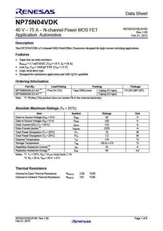
Preliminary Data Sheet NP75N04VDK R07DS1015EJ0100 40 V 75 A N-channel Power MOS FET Rev.1.00 Application Automotive Feb 21, 2013 Description The NP75N04VDK is N-channel MOS Field Effect Transistors designed for high current switching applications. Features Super low on-state resistance RDS(on) = 5.7 m MAX. (VGS = 10 V, ID = 38 A) Low Ciss Ciss = 1630 pF
np75n04vuk.pdf
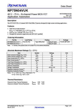
Preliminary Data Sheet NP75N04VUK R07DS0954EJ0100 40 V 75 A N-channel Power MOS FET Rev.1.00 Application Automotive Nov 20, 2012 Description The NP75N04VUK is N-channel MOS Field Effect Transistor designed for high current switching applications. Features Super low on-state resistance RDS(on) = 5.7 m MAX. (VGS = 10 V, ID = 38 A) Low Ciss Ciss = 1630 pF T
fdms015n04b.pdf
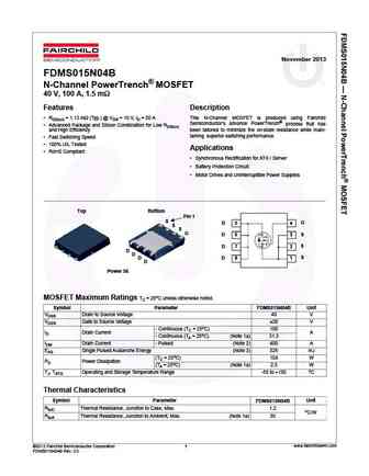
November 2013 FDMS015N04B N-Channel PowerTrench MOSFET 40 V, 100 A, 1.5 m Features Description RDS(on) = 1.13 m (Typ.) @ VGS = 10 V, ID = 50 A This N-Channel MOSFET is produced using Fairchild Advanced Package and Silicon Combination for Low RDS(on) Semiconductor s advance PowerTrench process that has and High Efficiency been tailored to minimize the on-state resistance
sup85n04-04 sub85n04-04.pdf
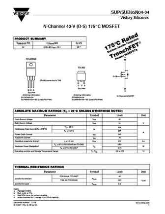
SUP/SUB85N04-04 Vishay Siliconix N-Channel 40-V (D-S) 175_C MOSFET PRODUCT SUMMARY V(BR)DSS (V) rDS(on) (W) ID (A) 40 0.004 @ VGS = 10 V 85 a D TO-220AB TO-263 G DRAIN connected to TAB G D S Top View G D S S Top View Ordering Information Ordering Information N-Channel MOSFET SUP85N04-04 SUB85N04-04 SUP85N04-04 E3 (Lead (Pb)-Free) SUB85N04-04 E3 (Lead (Pb)-Free) ABSOLUTE
sum75n04.pdf
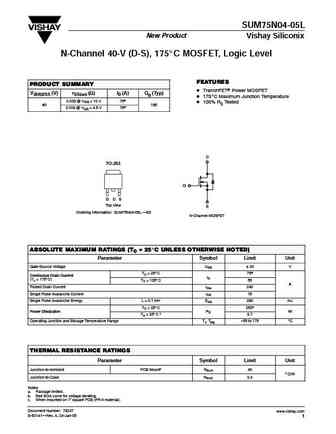
SUM75N04-05L New Product Vishay Siliconix N-Channel 40-V (D-S), 175_C MOSFET, Logic Level FEATURES PRODUCT SUMMARY D TrenchFETr Power MOSFET V(BR)DSS (V) rDS(on) (W) ID (A) Qg (Typ) D 175_C Maximum Junction Temperature 0.005 @ VGS = 10 V 75a D 100% Rg Tested 40 130 40 130 0.006 @ VGS = 4.5 V 75a D TO-263 G G D S Top View S Ordering Information SUM75N04-05L E3 N-Channel
sup85n04-03 sub85n04-03.pdf
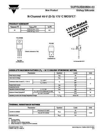
SUP/SUB85N04-03 New Product Vishay Siliconix N-Channel 40-V (D-S) 175_C MOSFET PRODUCT SUMMARY V(BR)DSS (V) rDS(on) (W) ID (A) 0.0035 @ VGS = 10 V a 40 85 a 40 85 0.0053 @ VGS = 4.5 V D TO-220AB TO-263 G DRAIN connected to TAB G D S Top View G D S S SUB85N04-03 Top View N-Channel MOSFET SUP85N04-03 ABSOLUTE MAXIMUM RATINGS (TC = 25_C UNLESS OTHERWISE NOTED) Parameter Sy
sup75n04-05l sub75n04-05l.pdf
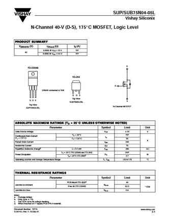
SUP/SUB75N04-05L Vishay Siliconix N-Channel 40-V (D-S), 175_C MOSFET, Logic Level PRODUCT SUMMARY V(BR)DSS (V) rDS(on) (W) ID (A) 0.0055 @ VGS = 10 V 75a 40 0.0065 @ VGS = 4.5 V 75a D TO-220AB TO-263 G DRAIN connected to TAB G D S Top View G D S S SUB75N04-05L Top View N-Channel MOSFET SUP75N04-05L ABSOLUTE MAXIMUM RATINGS (TC = 25_C UNLESS OTHERWISE NOTED) Parameter Symbo
sup85n04-03.pdf

SUP/SUB85N04-03 New Product Vishay Siliconix N-Channel 40-V (D-S) 175_C MOSFET PRODUCT SUMMARY V(BR)DSS (V) rDS(on) (W) ID (A) 0.0035 @ VGS = 10 V a 40 85 a 40 85 0.0053 @ VGS = 4.5 V D TO-220AB TO-263 G DRAIN connected to TAB G D S Top View G D S S SUB85N04-03 Top View N-Channel MOSFET SUP85N04-03 ABSOLUTE MAXIMUM RATINGS (TC = 25_C UNLESS OTHERWISE NOTED) Parameter Sy
sud25n04-25 sud25n04.pdf
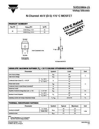
SUD25N04-25 Vishay Siliconix N-Channel 40-V (D-S) 175_C MOSFET PRODUCT SUMMARY VDS (V) rDS(on) (W) ID (A) 0.025 @ VGS = 10 V 25 40 0.040 @ VGS = 4.5 V 20 D TO-252 G Drain Connected to Tab G D S Top View Order Number S SUD25N04-25 N-Channel MOSFET ABSOLUTE MAXIMUM RATINGS (TA = 25_C UNLESS OTHERWISE NOTED) Parameter Symbol Limit Unit Drain-Source Voltage VDS 40 V Gate-Sour
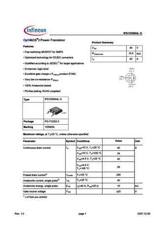
ipd105n04l.pdf
pe % # ! % (>.;?6?@ %>E Features V 4 D Q 2CD CG D49 ?8 ') - . 7@B -'*- R 1 m D n) m x Q ) AD > J65 D649?@=@8I 7@B 4@?F6BD6BC I 4 D 1) Q + E2= 7 65 244@B5 ?8 D@ $ 7@B D2B86D 2AA= 42D @?C Q ( 492??6= =@8 4 =6F6= Q H46==6?D 82D6 492B86 H R AB@5E4D ) ' D n) Q /6BI =@G @? B6C CD2?46 R D n) Q F2=2?496 D6CD65 Q *3 7B66 A=2D ?8 , @"- 4@>A= 2?D Type #
iauc100n08s5n043.pdf
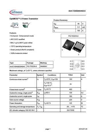
IAUC100N08S5N043 OptiMOS -5 Power-Transistor Product Summary VDS 80 V RDS(on) 4.3 mW ID 100 A Features N-channel - Enhancement mode PG-TDSON-8 AEC Q101 qualified MSL1 up to 260 C peak reflow 175 C operating temperature Green product (RoHS compliant) 1 100% Avalanche tested 1 Type Package Marking PG-TDSON-8 5N08043 IAUC100N08S5N043 Maximum ratings,
ipp015n04n ipb015n04n.pdf
pe ## ! ! # ! ! D # A0;53E;A@D R ' 5 3@@7> @AC?3> >7G7> R I57>>7@E 93E7 5 3C97 I BCA6F5E ( & D n) R .7CJ >AH A@ C7D;DE3@57 D n) R G3>3@5 7 E7DE76 R )4 8C77 B>3E;@9 + A", 5A?B>;3@E R "
ipb015n04l.pdf
pe $ " E $;B1= '=- >5>?;= $=;0@/? &@99-=D Features 4 D S 4EF EI
ipp015n04n6 ipb015n04n6.pdf

pe ## ! ! # ! ! D # A0;53E;A@D R ' 5 3@@7> @AC?3> >7G7> R I57>>7@E 93E7 5 3C97 I BCA6F5E ( & D n) R .7CJ >AH A@ C7D;DE3@57 D n) R G3>3@5 7 E7DE76 R )4 8C77 B>3E;@9 + A", 5A?B>;3@E R "
ipp015n04ng ipb015n04ng.pdf

pe ## ! ! # ! ! D # A0;53E;A@D R ' 5 3@@7> @AC?3> >7G7> R I57>>7@E 93E7 5 3C97 I BCA6F5E ( & D n) R .7CJ >AH A@ C7D;DE3@57 D n) R G3>3@5 7 E7DE76 R )4 8C77 B>3E;@9 + A", 5A?B>;3@E R "
ipb015n04lg ipb015n04l .pdf

pe $ " E $;B1= '=- >5>?;= $=;0@/? &@99-=D Features 4 D S 4EF EI
bsb015n04nx3g.pdf
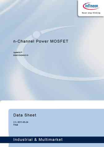
n-Channel Power MOSFET OptiMOS BSB015N04NX3 G Data Sheet 2.3, 2011-05-24 Final Industrial & Multimarket OptiMOS Power-MOSFET BSB015N04NX3 G 1 Description OptiMOS 40V products are class leading power MOSFETs for highest power density and energy efficient solutions. Ultra low gate- and output charges together with lowest on state resistance in small footprint packages make
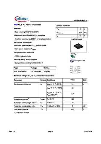
bsz025n04ls.pdf
MOSFET Metal Oxide Semiconductor Field Effect Transistor OptiMOSTM OptiMOSTM Power-MOSFET, 40 V BSZ025N04LS Data Sheet Rev. 2.1 Final Power Management & Multimarket OptiMOSTM Power-MOSFET, 40 V BSZ025N04LS TSDSON-8 FL 1 Description (enlarged source interconnection) Features Optimized for synchronous rectification Very low on-resistance R DS(on) 100% avalanche test
ipd75n04s4-06 ipd75n04s4-06 ds 1 1.pdf
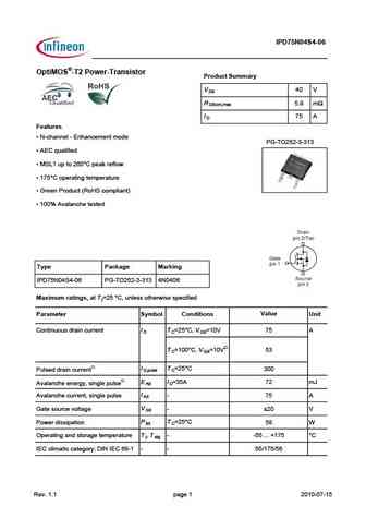
IPD75N04S4-06 OptiMOS -T2 Power-Transistor Product Summary V 40 V DS R 5.9 m DS(on),max I 75 A D Features N-channel - Enhancement mode PG-TO252-3-313 AEC qualified MSL1 up to 260 C peak reflow 175 C operating temperature Green Product (RoHS compliant) 100% Avalanche tested Type Package Marking IPD75N04S4-06 PG-TO252-3-313 4N0406 Maximum ratings,
ipp065n04n.pdf
pe $$ " " $;B1= '=- >5>?;= $=;0@/? &@99-=D Features 4 D R 3DE DH;E5 ;@9 &( , - 8AC ,&), m , A@ ?3I R ( BE;?;K76 E75 @A>A9J 8AC 5A@G7CE7CD D 1) R * F3>;8;76 355AC6;@9 EA $ 8AC E3C97E 3BB>;53E;A@D R ' 5 3@@7> @AC?3> >7G7> R I57>>7@E 93E7 5 3C97 I BCA6F5E ( & D n) R .7CJ >AH A@ C7D;DE3@57 D n) R G3>3@5 7 E7DE76 R )4 8C77 B>3E;@9 + A", 5A?B>;3@E Type #)) ' ' !
bsc035n04lsg.pdf
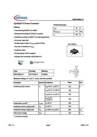
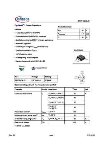
BSC035N04LS G OptiMOS 3 Power-Transistor Product Summary Features V 40 V DS Fast switching MOSFET for SMPS R 3.5 m DS(on),max Optimized technology for DC/DC converters I 100 A D Qualified according to JEDEC1) for target applications PG-TDSON-8 N-channel; Logic level Excellent gate charge x R product (FOM) DS(on) Very low on-resistance R DS(on)
ipb075n04l.pdf
pe % # ! % (>.;?6?@ %>E Features 4 D Q 2CD CG D49 ?8 ') - . 7@B -'*- 7 m D n) m x Q ) AD > J65 D649?@=@8I 7@B 4@?F6BD6BC D 1) Q + E2= 7 65 244@B5 ?8 D@ $ 7@B D2B86D 2AA= 42D @?C Q ( 492??6= =@8 4 =6F6= Q H46==6?D 82D6 492B86 H AB@5E4D ) ' D n) Q /6BI =@G @? B6C CD2?46 G O D n) Q F2=2?496 D6CD65 Q *3 7B66 A=2D ?8 , @"- 4@>A= 2?D Q "2=@86?
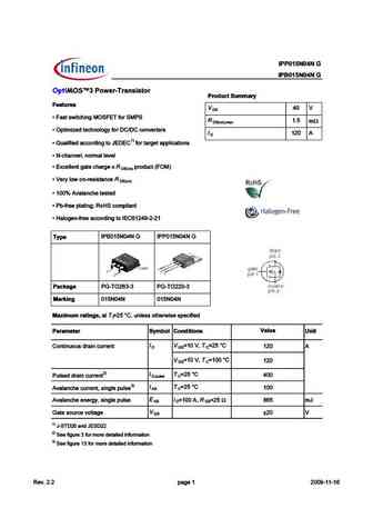
ipp45n04s4l-08 ipb45n04s4l-08 ipi45n04s4l-08.pdf
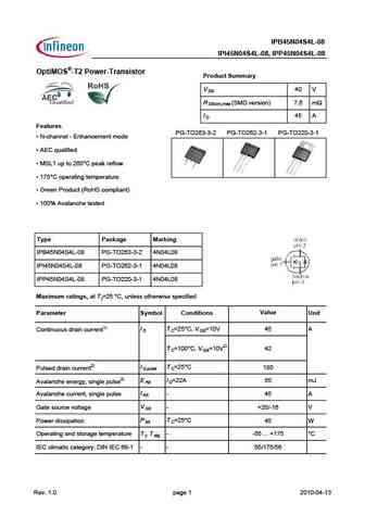
IPB45N04S4L-08 IPI45N04S4L-08, IPP45N04S4L-08 OptiMOS -T2 Power-Transistor Product Summary V 40 V DS R (SMD version) 7.6 m DS(on),max I 45 A D Features PG-TO263-3-2 PG-TO262-3-1 PG-TO220-3-1 N-channel - Enhancement mode AEC qualified MSL1 up to 260 C peak reflow 175 C operating temperature Green Product (RoHS compliant) 100% Avalanche tested Typ
nvbls0d5n04m8.pdf
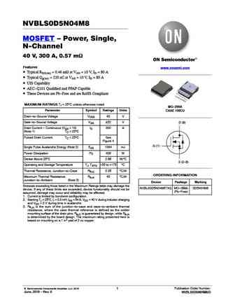
NVBLS0D5N04M8 MOSFET Power, Single, N-Channel 40 V, 300 A, 0.57 mW Features www.onsemi.com Typical RDS(on) = 0.46 mW at VGS = 10 V, ID = 80 A Typical Qg(tot) = 220 nC at VGS = 10 V, ID = 80 A UIS Capability AEC-Q101 Qualified and PPAP Capable These Devices are Pb-Free and are RoHS Compliant MAXIMUM RATINGS TJ = 25 C unless otherwise noted MO-299A Parameter
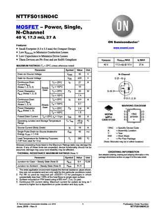
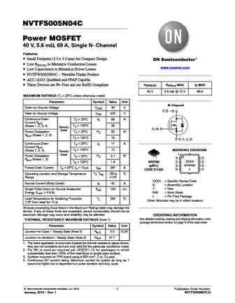
nttfs005n04c.pdf
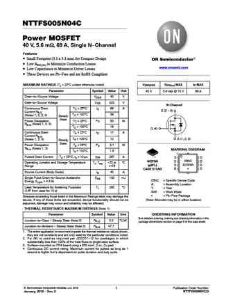
NTTFS005N04C Power MOSFET 40 V, 5.6 mW, 69 A, Single N-Channel Features Small Footprint (3.3 x 3.3 mm) for Compact Design Low RDS(on) to Minimize Conduction Losses www.onsemi.com Low Capacitance to Minimize Driver Losses These Devices are Pb-Free and are RoHS Compliant V(BR)DSS RDS(on) MAX ID MAX MAXIMUM RATINGS (TJ = 25 C unless otherwise noted) Parameter Symbol Val
nvtfs015n04c.pdf
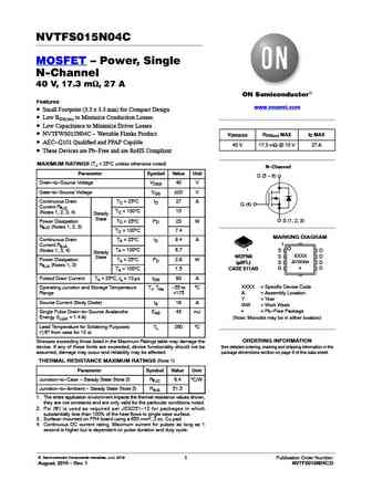
NVTFS015N04C MOSFET Power, Single N-Channel 40 V, 17.3 mW, 27 A Features www.onsemi.com Small Footprint (3.3 x 3.3 mm) for Compact Design Low RDS(on) to Minimize Conduction Losses Low Capacitance to Minimize Driver Losses NVTFWS015N04C - Wettable Flanks Product V(BR)DSS RDS(on) MAX ID MAX AEC-Q101 Qualified and PPAP Capable 40 V 17.3 mW @ 10 V 27 A These
fdms015n04b.pdf

Is Now Part of To learn more about ON Semiconductor, please visit our website at www.onsemi.com Please note As part of the Fairchild Semiconductor integration, some of the Fairchild orderable part numbers will need to change in order to meet ON Semiconductor s system requirements. Since the ON Semiconductor product management systems do not have the ability to manage part nomenclatur
njvnjd35n04.pdf
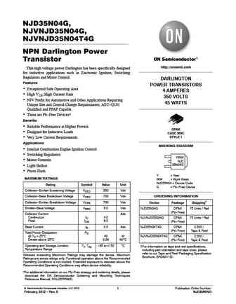
NJD35N04G, NJVNJD35N04G, NJVNJD35N04T4G NPN Darlington Power Transistor http //onsemi.com This high voltage power Darlington has been specifically designed for inductive applications such as Electronic Ignition, Switching Regulators and Motor Control. DARLINGTON Features POWER TRANSISTORS Exceptional Safe Operating Area 4 AMPERES High VCE; High Current Gain 350 VOLTS
nttfs015n04c.pdf
NTTFS015N04C MOSFET Power, Single, N-Channel 40 V, 17.3 mW, 27 A Features www.onsemi.com Small Footprint (3.3 x 3.3 mm) for Compact Design Low RDS(on) to Minimize Conduction Losses Low Capacitance to Minimize Driver Losses These Devices are Pb-Free and are RoHS Compliant V(BR)DSS RDS(on) MAX ID MAX 40 V 17.3 mW @ 10 V 27 A MAXIMUM RATINGS (TJ = 25 C unless otherw
nvtfs005n04c.pdf
NVTFS005N04C Power MOSFET 40 V, 5.6 mW, 69 A, Single N-Channel Features Small Footprint (3.3 x 3.3 mm) for Compact Design Low RDS(on) to Minimize Conduction Losses www.onsemi.com Low Capacitance to Minimize Driver Losses NVTFWS005N04C - Wettable Flanks Product AEC-Q101 Qualified and PPAP Capable V(BR)DSS RDS(on) MAX ID MAX These Devices are Pb-Free and are RoH
njd35n04t4g.pdf

NJD35N04G, NJVNJD35N04G, NJVNJD35N04T4G NPN Darlington Power Transistor http //onsemi.com This high voltage power Darlington has been specifically designed for inductive applications such as Electronic Ignition, Switching Regulators and Motor Control. DARLINGTON Features POWER TRANSISTORS Exceptional Safe Operating Area 4 AMPERES High VCE; High Current Gain 350 VOLTS
njd35n04g.pdf

NJD35N04G, NJVNJD35N04G, NJVNJD35N04T4G NPN Darlington Power Transistor http //onsemi.com This high voltage power Darlington has been specifically designed for inductive applications such as Electronic Ignition, Switching Regulators and Motor Control. DARLINGTON Features POWER TRANSISTORS Exceptional Safe Operating Area 4 AMPERES High VCE; High Current Gain 350 VOLTS
cjab25n04.pdf
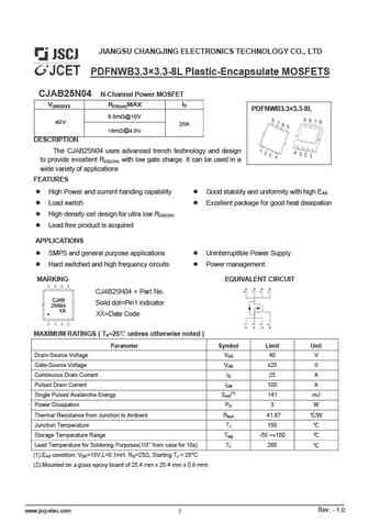
JIANGSU CHANGJING ELECTRONICS TECHNOLOGY CO., LTD PDFNWB3.3 3.3-8L Plastic-Encapsulate MOSFETS CJAB25N04 N-Channel Power MOSFET ID V(BR)DSS RDS(on)MAX PDFNWB3.3 3.3-8L 9.5m @10V 40V 25A 16m @4.5V DESCRIPTION The CJAB25N04 uses advanced trench technology and design to provide excellent RDS(ON) with low gate charge. It can be used in a wide variety of applications FEAT
mtb25n04j3.pdf
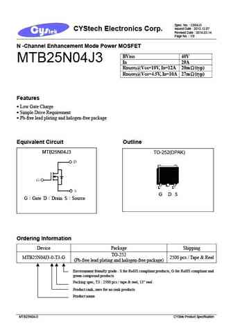
Spec. No. C884J3 Issued Date 2012.12.07 CYStech Electronics Corp. Revised Date 2014.03.14 Page No. 1/9 N -Channel Enhancement Mode Power MOSFET BVDSS 40V MTB25N04J3 ID 29A RDS(ON)@VGS=10V, ID=12A 20m (typ) RDS(ON)@VGS=4.5V, ID=10A 27m (typ) Features Low Gate Charge Simple Drive Requirement Pb-free lead plating and halogen-free package Equivalen
mtb35n04j3.pdf
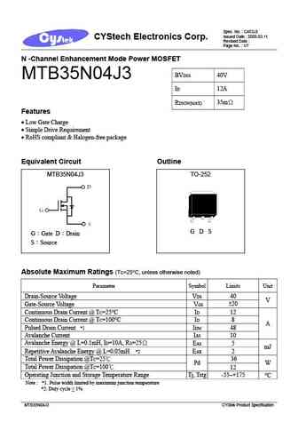
Spec. No. C453J3 Issued Date 2009.03.11 CYStech Electronics Corp. Revised Date Page No. 1/7 N -Channel Enhancement Mode Power MOSFET BVDSS 40V MTB35N04J3 ID 12A 35m RDSON(MAX) Features Low Gate Charge Simple Drive Requirement RoHS compliant & Halogen-free package Equivalent Circuit Outline MTB35N04J3 TO-252 G D S G Gate D Drain S S
sdu05n04 sdd05n04.pdf
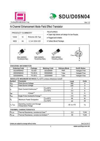
Green Product SDU/D05N04 a S mHop Microelectronics C orp. Ver 1.2 N-Channel Enhancement Mode Field Effect Transistor FEATURES PRODUCT SUMMARY Super high dense cell design for low RDS(ON). VDSS ID RDS(ON) ( ) Typ Rugged and reliable. 400V 4A 2.1 @ VGS=10V Suface Mount Package. D G S SDU SERIES SDD SERIES SDD SERIES TO-252(D-PAK) TO-251S(I-PAK) TO-251L(I-PAK) ORDERING INFORMATI
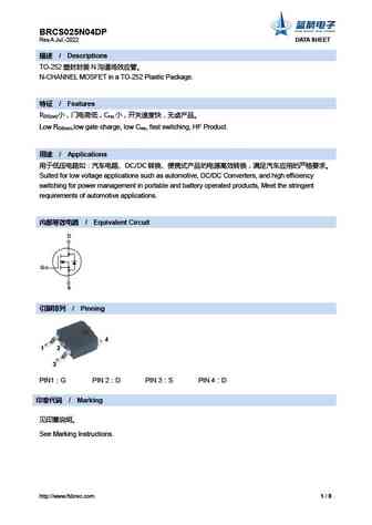
brcs025n04dp.pdf
BRCS025N04DP Rev.A Jul.-2022 DATA SHEET / Descriptions TO-252 N N-CHANNEL MOSFET in a TO-252 Plastic Package. / Features R C DS(on) rss Low RDS(on),low gate charge, low Crss, fast switching, HF Product. / Applications DC/D
brcs015n04szc.pdf
BRCS015N04SZC Rev.B Feb.-2023 DATA SHEET / Descriptions PDFN5 6 N N-Channel MOSFET in a PDFN5 6 Plastic Package. / Features Low R to minimize conductive loss;low Gate Charge for fast switching;Low Thermal resistance; DS(ON
dh035n04 dhf035n04 dhi035n04 dhe035n04 dhb035n04 dhd035n04.pdf
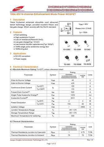
DH035N04/DHF035N04/DHI035N04/ DHE035N04/DHB035N04/DHD035N04 155A 40V N-channel Enhancement Mode Power MOSFET 1 Description These N-channel enhanced vdmosfets used advanced 2 D V = 40V DSS trench technology design, provided excellent Rdson and low gate charge. Which accords with the RoHS standard. R = 2.3m DS(on) (TYP) G 1 2 Features I = 155A D 3 S Fast switching High
dhp035n04.pdf
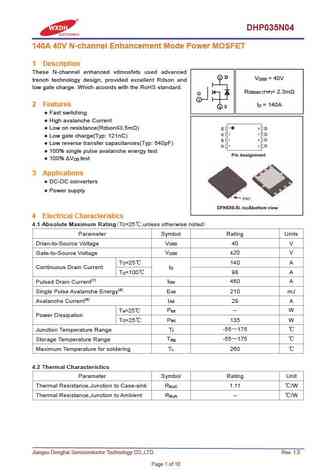
DHP035N04 140A 40V N-channel Enhancement Mode Power MOSFET 1 Description These N-channel enhanced vdmosfets used advanced 2 D V = 40V DSS trench technology design, provided excellent Rdson and low gate charge. Which accords with the RoHS standard. R = 2.3m DS(on) (TYP) G 1 2 Features I = 140A D 3 S Fast switching High avalanche Current Low on resistance(Rdson 3
dh065n04p.pdf
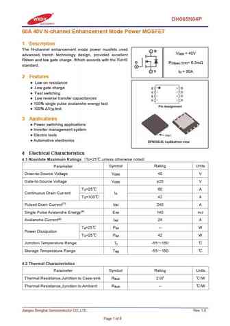
DH065N04P 60A 40V N-channel Enhancement Mode Power MOSFET 1 Description The N-channel enhancement mode power mosfets used 2 D V = 40V DSS advanced trench technology design, provided excellent Rdson and low gate charge. Which accords with the RoHS G R = 6.3m DS(on) (TYP) standard. 1 3 S I = 60A D 2 Features Low on resistance Low gate charge Fast switching L
dsd065n04la.pdf
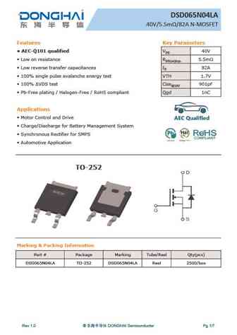
DSD065N04LA 40V/5.5m /82A N-MOSFET Features Key Parameters AEC-Q101 qualified VDS 40V Low on resistance RDS(on)typ. 5.5m Low reverse transfer capacitances ID 82A 100% single pulse avalanche energy test VTH 1.7V 100% VDS test Ciss@10V 901pF Pb-Free plating / Halogen-Free / RoHS compliant Qgd 1nC Applications Motor Control and Drive Charge/Discharge
dh065n04 dh065n04f dh065n04i dh065n04e dh065n04b dh065n04d.pdf
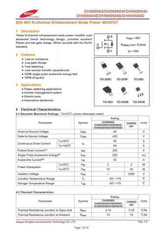
DH065N04/DH065N04FDH065N04I/ DH065N04E/DH065N04B/DH065N04D 80A 40V N-channel Enhancement Mode Power MOSFET 1 Description These N-channel enhancement mode power mosfets used 2 D V = 40V DSS advanced trench technology design, provided excellent Rdson and low gate charge. Which accords with the RoHS G R = 6.0m DS(on) (TYP) standard. 1 3 S I = 80A D 2 Features Low on resist
dh025n04 dh025n04f dh025n04i dh025n04e dh025n04b dh025n04d.pdf
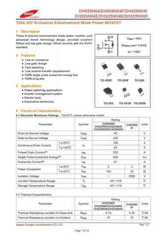
DH025N04/DH025N04F/DH025N04I DH025N04E/DH025N04B/DH025N04D 130A 40V N-channel Enhancement Mode Power MOSFET 1 Description These N-channel enhancement mode power mosfets used 2 D V = 40V DSS advanced trench technology design, provided excellent Rdson and low gate charge. Which accords with the RoHS G R = 2.8m DS(on) (TYP) standard. 1 3 S I = 130A D 2 Features Low on resi
dh045n04 dh045n04f dh045n04i dh045n04e dh045n04b dh045n04d.pdf
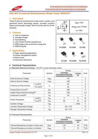
DH045N04/DH045N04FDH045N04I/ DH045N04E/DH045N04B/DH045N04D 90A 40V N-channel Enhancement Mode Power MOSFET 1 Description These N-channel enhancement mode power mosfets used 2 D V = 40V DSS advanced trench technology design, provided excellent Rdson and low gate charge. Which accords with the RoHS G R = 5.5m DS(on) (TYP) standard. 1 3 S I = 90A D 2 Features Low on resist
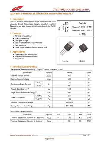
dte025n04na dtg025n04na.pdf
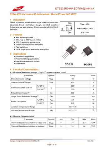
DTE025N04NA&DTG025N04NA 220A 40V N-channel Enhancement Mode Power MOSFET 1 Description These N-channel enhancement mode power mosfets used 2 D V = 40V DSS advanced trench technology design, provided excellent Rdson and low gate charge. Which accords with the RoHS G R = 2.1m DS(on) (TYP) standard. 1 3 S I = 220A D 2 Features AEC Q101 qualified MSL1 up to 260 C peak
dh045n04p.pdf

DH045N04P 80A 40V N-channel Enhancement Mode Power MOSFET 1 Description These N-channel enhancement mode power mosfets used 2 D V = 40V DSS advanced trench technology design, provided excellent Rdson and low gate charge. Which accords with the RoHS G R = 5.7m DS(on) (TYP) standard. 1 3 S I = 80A D 2 Features Low on resistance Low gate charge Fast switching
blm055n04-d.pdf
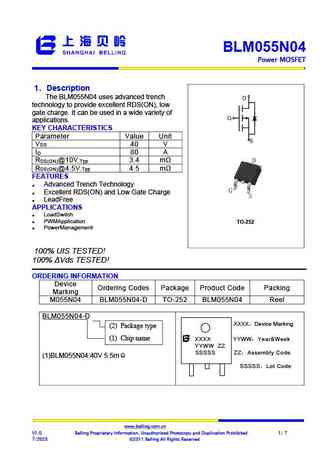
BLM055N04 Power MOSFET 1 Description Step-Down Converter The BLM055N04 uses advanced trench , technology to provide excellent RDS(ON), low gate charge. It can be used in a wide variety of applications. KEY CHARACTERISTICS Parameter Value Unit V 40 V DS I 80 A D R .Typ 3.4 m DS(ON)@10V R .Typ 4.5 m DS(ON)@4.5V FEATURES Advanced Trench Technolog
blm075n04-d.pdf
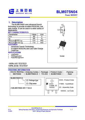
BLM075N04 Power MOSFET 1 Description Step-Down Converter The BLM075N04 uses advanced trench , technology to provide excellent RDS(ON), low gate charge. It can be used in a wide variety of applications. KEY CHARACTERISTICS Parameter Value Unit V 40 V DS I 60 A D R .Typ 5.4 m DS(ON)@10V R .Typ 7.8 m DS(ON)@4.5V FEATURES Advanced Trench Technolog
swk15n04v swha15n04v.pdf
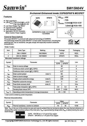
SW15N04V N-channel Enhanced mode SOP8/DFN5*6 MOSFET Features BVDSS 40V DFN5*6 SOP8 5 ID 15A High ruggedness 6 1 8 7 Low RDS(ON) (Typ 6.5m )@VGS=4.5V 2 7 8 RDS(ON) 6.5m @ VGS=4.5V 6 3 (Typ 5.8m )@VGS=10V 4 3 4 5 5.8m @ VGS=10V Low Gate Charge (Typ 49nC) 2 1 Improved dv/dt Capability D 100% Avalanche Tested
hrp35n04k.pdf
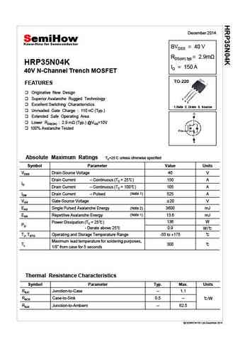
December 2014 BVDSS = 40 V RDS(on) typ = 2.9m HRP35N04K ID = 150 A 40V N-Channel Trench MOSFET TO-220 FEATURES Originative New Design Superior Avalanche Rugged Technology 1 2 3 Excellent Switching Characteristics 1.Gate 2. Drain 3. Source Unrivalled Gate Charge 110 nC (Typ.) Extended Safe Operating Area Lower RDS(ON) 2.9 m (Typ.
wmo75n04t1.pdf
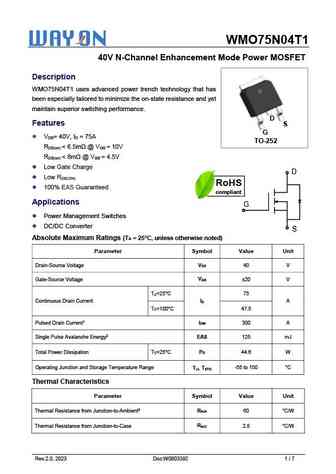
WMO75N04T1 40V N-Channel Enhancement Mode Power MOSFET Description WMO75N04T1 uses advanced power trench technology that has been especially tailored to minimize the on-state resistance and yet maintain superior switching performance. D Features S G V = 40V, I = 75A DS D TO-252 R
wmq55n04t1.pdf
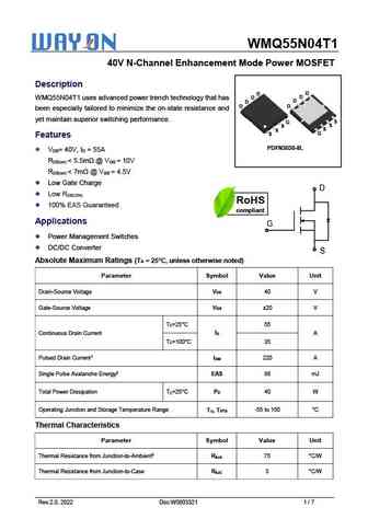
WMQ55N04T1 40V N-Channel Enhancement Mode Power MOSFET Description D D D WMQ55N04T1 uses advanced power trench technology that has D D D D D been especially tailored to minimize the on-state resistance and yet maintain superior switching performance. S G S S S S G S Features PDFN3030-8L V = 40V, I = 55A DS D R
jmtq055n04a.pdf
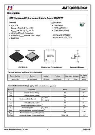
JMTQ055N04A Description JMT N-channel Enhancement Mode Power MOSFET Features Applications 40V, 70A Load Switch RDS(ON)
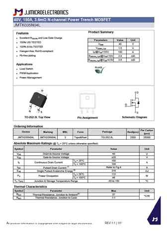
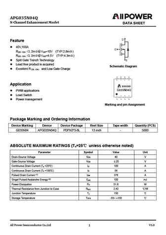
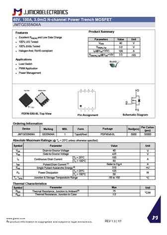
jmtc035n04a.pdf
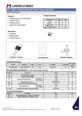
40V, 150A, 3.4m N-channel Power Trench MOSFET JMTC035N04A Product Summary Features Excellent RDS(ON) and Low Gate Charge Parameters Value Unit 100% UIS Tested VDSS 40 V 100% Vds Tested VGS(th)_Typ 2.8 V Halogen-free; RoHS-compliant ID(@VGS=10V) 150 A RDS(ON)_Typ(@VGS=10V 3.4 mW Applications Load Switch PWM Application Power Management D G S
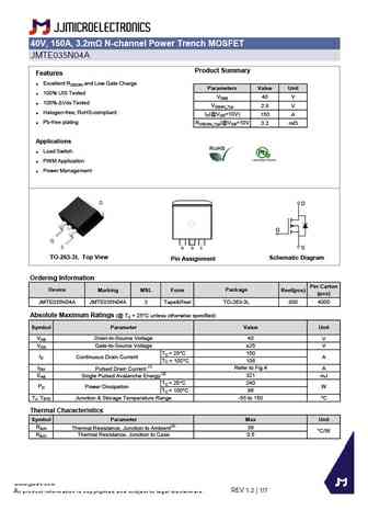
jmte025n04d.pdf
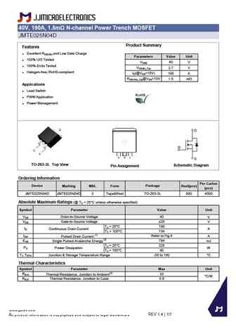
40V, 190A, 1.5m N-channel Power Trench MOSFET JMTE025N04D Product Summary Features Excellent RDS(ON) and Low Gate Charge Parameters Value Unit 100% UIS Tested VDSS 40 V 100% Vds Tested VGS(th)_Typ 2.7 V Halogen-free; RoHS-compliant ID(@VGS=10V) 190 A RDS(ON)_Typ@VGS=10V 1.5 mW Applications Load Switch PWM Application Power Management D G S T
jmtc025n04d.pdf
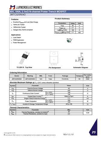
40V, 190A, 2.1m N-channel Power Trench MOSFET JMTC025N04D Product Summary Features Excellent RDS(ON) and Low Gate Charge Parameters Value Unit 100% UIS Tested VDSS 40 V 100% Vds Tested VGS(th)_Typ 2.7 V Halogen-free; RoHS-compliant ID(@VGS=10V) 190 A RDS(ON)_Typ(@VGS=10V 2.1 mW Applications Load Switch PWM Application Power Management D G S T
jmte035n04a.pdf
40V, 150A, 3.2m N-channel Power Trench MOSFET JMTE035N04A Product Summary Features Excellent RDS(ON) and Low Gate Charge Parameters Value Unit 100% UIS Tested VDSS 40 V 100% Vds Tested VGS(th)_Typ 2.8 V Halogen-free; RoHS-compliant ID(@VGS=10V) 150 A Pb-free plating RDS(ON)_Typ(@VGS=10V 3.2 mW Applications Load Switch PWM Application Power M
jmtg035n04l.pdf
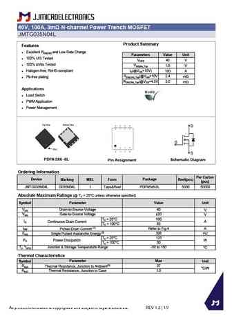
40V, 100A, 3m N-channel Power Trench MOSFET JMTG035N04L Product Summary Features Excellent RDS(ON) and Low Gate Charge Parameters Value Unit 100% UIS Tested VDSS 40 V 100% Vds Tested VGS(th)_Typ 1.5 V Halogen-free; RoHS-compliant ID(@VGS=10V) 100 A RDS(ON)_Typ(@VGS=10V 2.4 mW Pb-free plating RDS(ON)_Typ(@VGS=4.5V 3.0 mW Applications Load Switch P
jmtg055n04a.pdf
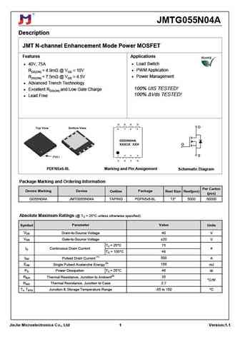
JMTG055N04A Description JMT N-channel Enhancement Mode Power MOSFET Features Applications 40V, 75A Load Switch RDS(ON)
jmtg035n04a.pdf
40V, 100A, 3.0m N-channel Power Trench MOSFET JMTG035N04A Product Summary Features Excellent RDS(ON) and Low Gate Charge Parameters Value Unit 100% UIS Tested VDSS 40 V 100% Vds Tested VGS(th)_Typ 3.0 V Halogen-free; RoHS-compliant ID(@VGS=10V) 100 A RDS(ON)_Typ(@VGS=10V 3.0 mW Applications Load Switch PWM Application Power Management D G S P
htn035n04p.pdf
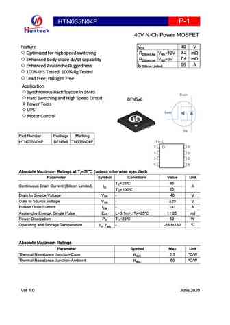
HTN035N04P P-1 40V N-Ch Power MOSFET 40 V Feature VDS 3.2 Optimized for high speed switching RDS(on),typ VGS=10V mW 7.4 RDS(on),typ VGS=6V mW Enhanced Body diode dv/dt capability 95 A ID (Sillicon Limited) Enhanced Avalanche Ruggedness 100% UIS Tested, 100% Rg Tested Lead Free, Halogen Free Application Synchronous Rectification in SMPS Drain Hard Swi
yjq35n04a.pdf
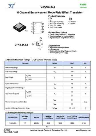
RoHS COMPLIANT YJQ35N04A N-Channel Enhancement Mode Field Effect Transistor Product Summary V 40 V DS I 35 A D R ( at V = 10V) 8.0mohm DS(ON) GS R ( at V = 4.5V) 13mohm DS(ON) GS 100% UIS Tested 100% VDS Tested General Description Trench Power LV MOSFET technology Excellent package for heat dissipation High density c
s85n048s.pdf
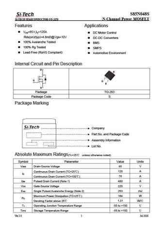
S85N048S SI-TECH SEMICONDUCTOR CO.,LTD N-Channel Power MOSFET Features Applications VDS=85V,ID=120A DC Motor Control Rds(on)(typ)=4.8m @Vgs=10V DC-DC Converters 100% Avalanche Tested BMS 100% Rg Tested SMPS Lead-Free (RoHS Compliant) Automotive Environment Internal Circuit and Pin Description D D G G
s85n042r s85n042s s85n042rn s85n042rp.pdf
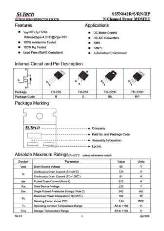
S85N042R/S/RN/RP SI-TECH SEMICONDUCTOR CO.,LTD N-Channel Power MOSFET Features Applications VDS=85V,ID=128A DC Motor Control Rds(on)(typ)=4.2m @Vgs=10V DC-DC Converters 100% Avalanche Tested BMS 100% Rg Tested SMPS Lead-Free (RoHS Compliant) Automotive Environment Internal Circuit and Pin Description D D G G G G G D D
ipb015n04l.pdf
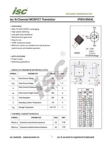
INCHANGE Semiconductor isc N-Channel MOSFET Transistor IPB015N04L FEATURES With TO-263( D2PAK ) packaging High speed switching Low gate input resistance Standard level gate drive Easy to use 100% avalanche tested Minimum Lot-to-Lot variations for robust device performance and reliable operation APPLICATIONS Power supply Switching applications ABSOLUTE MAXIM
ipb015n04n.pdf
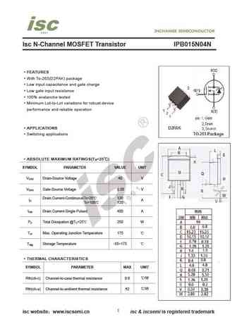
Isc N-Channel MOSFET Transistor IPB015N04N FEATURES With To-263(D2PAK) package Low input capacitance and gate charge Low gate input resistance 100% avalanche tested Minimum Lot-to-Lot variations for robust device performance and reliable operation APPLICATIONS Switching applications ABSOLUTE MAXIMUM RATINGS(T =25 ) a SYMBOL PARAMETER VALUE UNIT V Drain-Source Vo
ipp015n04n.pdf
INCHANGE Semiconductor isc N-Channel MOSFET Transistor IPP015N04N IIPP015N04N FEATURES Static drain-source on-resistance RDS(on) 1.5m Enhancement mode Fast Switching Speed 100% avalanche tested Minimum Lot-to-Lot variations for robust device performance and reliable operation DESCRITION reliable device for use in a wide variety of applications ABSOLUTE MAX
ap25n04s.pdf
AP25N04S 40V N-Channel Enhancement Mode MOSFET Description The AP25N04S uses advanced trench technology to provide excellent R , low gate charge and DS(ON) operation with gate voltages as low as 4.5V. This device is suitable for use as a Battery protection or in other Switching application. General Features V =40V I =25A DS D R
ap85n04nf.pdf
AP85N04NF 40V N-Channel Enhancement Mode MOSFET Description The AP85N04NF uses advanced trench technology to provide excellent R , low gate charge and DS(ON) operation with gate voltages as low as 4.5V. This device is suitable for use as a Battery protection or in other Switching application. General Features V = 40V I =100 A DS D R
ap65n04df.pdf
AP65N04DF 40V N-Channel Enhancement Mode MOSFET Description The AP65N04DF uses advanced trench technology to provide excellent R , low gate charge and DS(ON) operation with gate voltages as low as 4.5V. This device is suitable for use as a Battery protection or in other Switching application. General Features V = 40V I =65A DS D R
ap15n04s.pdf
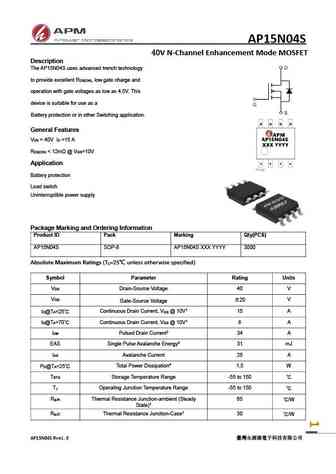
AP15N04S 40V N-Channel Enhancement Mode MOSFET Description The AP15N04S uses advanced trench technology to provide excellent R , low gate charge and DS(ON) operation with gate voltages as low as 4.5V. This device is suitable for use as a Battery protection or in other Switching application. General Features V = 40V I =15 A DS D R
ap5n04mi.pdf
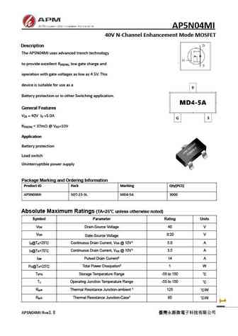
AP5N04MI 40V N-Channel Enhancement Mode MOSFET Description The AP5N04MI uses advanced trench technology to provide excellent R , low gate charge and DS(ON) operation with gate voltages as low as 4.5V. This device is suitable for use as a Battery protection or in other Switching application. General Features V = 40V I =5.0A DS D R
ap25n04d.pdf
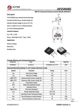
AP25N04D 40V N-Channel Enhancement Mode MOSFET Description The AP25N04D uses advanced trench technology to provide excellent R , low gate charge and DS(ON) operation with gate voltages as low as 4.5V. This device is suitable for use as a Battery protection or in other Switching application. General Features V = 40V I =25A DS D R
Другие MOSFET... SMF8N60 , SMF8N65 , SMT10N60 , SMT12N60 , SMT5N60 , SMT8N60 , 1H05 , 1H10 , P55NF06 , HA20N50 , HA20N60 , HA210N06 , HA25N50 , HA9N90 , HB100N08 , HP100N08 , HB3510P .
History: ASDM3010
History: ASDM3010
🌐 : EN ES РУ

Список транзисторов
Обновления
MOSFET: AUB062N08BG | AUB060N08AG | AUB056N10 | AUB056N08BGL | AUB050N085 | AUB050N055 | AUB045N12 | AUB045N10BT | AUB039N10 | AUB034N10 | AUB033N08BG | AUB026N085 | AUA062N08BG | AUA060N08AG | AUA056N08BGL | AUA039N10
Popular searches
rfp50n06 | bd140 datasheet | tip2955 | tip35 | 2sk117 | irf9540n datasheet | ss8050 | irfp4668