HM2306. Аналоги и основные параметры
Наименование производителя: HM2306
Тип транзистора: MOSFET
Полярность: N
Предельные значения
Pd ⓘ
- Максимальная рассеиваемая мощность: 1.4 W
|Vds|ⓘ - Максимально допустимое напряжение сток-исток: 30 V
|Vgs|ⓘ - Максимально допустимое напряжение затвор-исток: 12 V
|Id| ⓘ - Максимально допустимый постоянный ток стока: 5.8 A
Tj ⓘ - Максимальная температура канала: 150 °C
Электрические характеристики
tr ⓘ -
Время нарастания: 4.8 ns
Cossⓘ - Выходная емкость: 99 pf
RDSonⓘ - Сопротивление сток-исток открытого транзистора: 0.041 Ohm
Тип корпуса: SOT23
Аналог (замена) для HM2306
- подборⓘ MOSFET транзистора по параметрам
HM2306 даташит
..1. Size:355K cn hmsemi
hm2306.pdf 
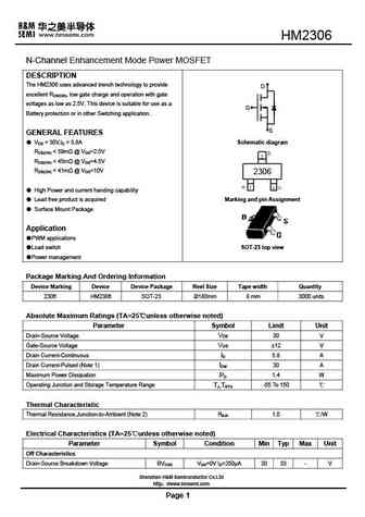
HM2306 N-Channel Enhancement Mode Power MOSFET DESCRIPTION The HM2306 uses advanced trench technology to provide D excellent RDS(ON), low gate charge and operation with gate voltages as low as 2.5V. This device is suitable for use as a G Battery protection or in other Switching application. S GENERAL FEATURES VDS = 30V,ID = 5.8A Schematic diagram RDS(ON)
9.1. Size:219K chenmko
chm2304gp.pdf 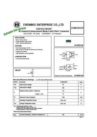
CHENMKO ENTERPRISE CO.,LTD CHM2304GP SURFACE MOUNT N-Channel Enhancement Mode Field Effect Transistor VOLTAGE 30 Volts CURRENT 2.8 Ampere APPLICATION * Servo motor control. * Power MOSFET gate drivers. * Other switching applications. SC-59/SOT-346 FEATURE * Small flat package. (SC-59 ) * High density cell design for extremely low RDS(ON). * Rugged and reliable. (2) * High sat
9.2. Size:132K chenmko
chm2301esgp.pdf 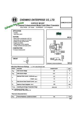
CHENMKO ENTERPRISE CO.,LTD CHM2301ESGP SURFACE MOUNT P-Channel Enhancement Mode Field Effect Transistor VOLTAGE 20 Volts CURRENT 2.8 Ampere APPLICATION * Po rtable * High speed switch FEATURE SOT-23 * Small surface mounting type. (SOT-23) * High density cell design for low RDS(ON) * Suitable for high packing density. * Rugged and reliable. (1) * High saturation current capabili
9.3. Size:178K chenmko
chm2308esgp.pdf 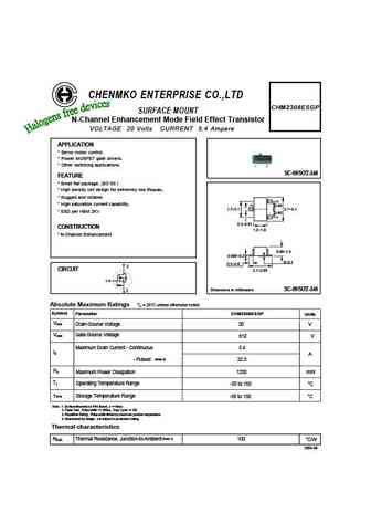
CHENMKO ENTERPRISE CO.,LTD CHM2308ESGP SURFACE MOUNT N-Channel Enhancement Mode Field Effect Transistor VOLTAGE 20 Volts CURRENT 5.4 Ampere APPLICATION * Servo motor control. * Power MOSFET gate drivers. * Other switching applications. SC-59/SOT-346 FEATURE * Small flat package. (SC-59 ) * High density cell design for extremely low RDS(ON). * Rugged and reliable. (2) * High s
9.4. Size:85K chenmko
chm2307gp.pdf 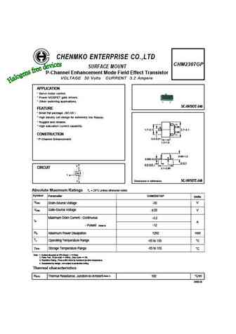
CHENMKO ENTERPRISE CO.,LTD CHM2307GP SURFACE MOUNT P-Channel Enhancement Mode Field Effect Transistor VOLTAGE 30 Volts CURRENT 3.2 Ampere APPLICATION * Servo motor control. * Power MOSFET gate drivers. * Other switching applications. SC-59/SOT-346 FEATURE * Small flat package. (SC-59 ) * High density cell design for extremely low RDS(ON). * Rugged and reliable. (2) * High sat
9.5. Size:97K chenmko
chm2305gp.pdf 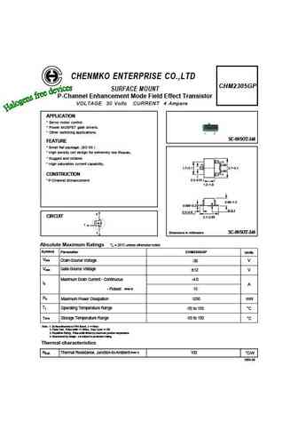
CHENMKO ENTERPRISE CO.,LTD CHM2305GP SURFACE MOUNT P-Channel Enhancement Mode Field Effect Transistor VOLTAGE 30 Volts CURRENT 4 Ampere APPLICATION * Servo motor control. * Power MOSFET gate drivers. * Other switching applications. SC-59/SOT-346 FEATURE * Small flat package. (SC-59 ) * High density cell design for extremely low RDS(ON). * Rugged and reliable. (2) * High satur
9.6. Size:1768K cn vbsemi
hm2301kr.pdf 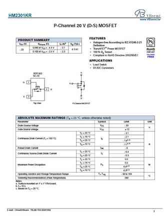
HM2301KR www.VBsemi.tw P-Channel 20 V (D-S) MOSFET FEATURES PRODUCT SUMMARY Halogen-free According to IEC 61249-2-21 VDS (V) RDS(on) ( )ID (A)c Qg (Typ.) Definition 0.080 at VGS = - 4.5 V - 3.1 TrenchFET Power MOSFET 4.3 nC - 20 0.100 at VGS = - 2.5 V - 2.3 100 % Rg Tested Compliant to RoHS Directive 2002/95/EC APPLICATIONS Load Switch DC/DC Convert
9.7. Size:1649K cn vbsemi
hm2305pr.pdf 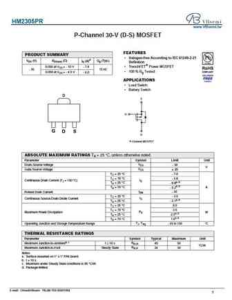
HM2305PR www.VBsemi.tw P-Channel 30-V (D-S) MOSFET FEATURES PRODUCT SUMMARY Halogen-free According to IEC 61249-2-21 VDS (V) RDS(on) ( ) ID (A)d Qg (Typ.) Definition 0.050 at VGS = - 10 V - 7.6 TrenchFET Power MOSFET - 30 13 nC 100 % Rg Tested 0.056 at VGS = - 4.5 V - 6.0 APPLICATIONS Load Switch Battery Switch D S G G D S D P-Channel MOSFET ABS
9.8. Size:1890K cn vbsemi
hm2300.pdf 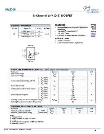
HM2300 www.VBsemi.tw N-Channel 20 V (D-S) MOSFET FEATURES PRODUCT SUMMARY Halogen-free According to IEC 61249-2-21 VDS (V) RDS(on) ( ) ID (A)e Qg (Typ.) Definition 0.028 at VGS = 4.5 V TrenchFET Power MOSFET 6a 100 % Rg Tested 20 0.042 at VGS = 2.5 V 6a 8.8 nC Compliant to RoHS Directive 2002/95/EC 0.050 at VGS = 1.8 V 5.6 APPLICATIONS DC/DC Convert
9.9. Size:572K cn hmsemi
hm2301a.pdf 
HM2301A P-Channel Enhancement Mode Power MOSFET DESCRIPTION D The HM2301A uses advanced trench technology to provide excellent RDS(ON), low gate charge and operation with gate G voltages as low as 2.5V. This device is suitable for use as a load switch or in PWM applications. S GENERAL FEATURES Schematic diagram VDS = -20V,ID = -3A RDS(ON)
9.10. Size:652K cn hmsemi
hm2301c.pdf 
HM2301 P-Channel Trench Power MOSFET General Description The HM2301 uses advanced trench technology to provide excellent R , low gate charge and operation with gate DS(ON) voltages as low as -2.5V. This device is suitable for use as a battery protection or in other switching application. Features Schematic Diagram VDS = -12V,ID =-2. A R
9.11. Size:512K cn hmsemi
hm2305b.pdf 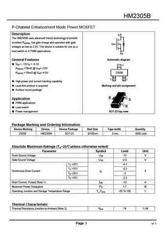
HM2305B P-Channel Enhancement Mode Power MOSFET Description D The HM2305B uses advanced trench technology to provide excellent RDS(ON), low gate charge and operation with gate G voltages as low as 2.5V. This device is suitable for use as a load switch or in PWM applications. S Schematic diagram General Features VDS = -12V,ID = -4.1A RDS(ON)
9.12. Size:873K cn hmsemi
hm2309.pdf 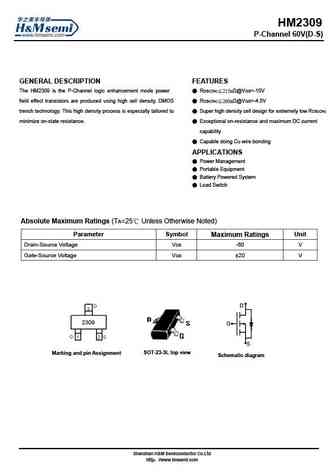
HM2309 P-Channel 60V(D-S) GENERAL DESCRIPTION FEATURES RDS(ON) 215m @VGS=-10V The HM2309 is the P-Channel logic enhancement mode power RDS(ON) 260m @VGS=-4.5V field effect transistors are produced using high cell density, DMOS Super high density cell design for extremely low RDS(ON) trench technology. This high density process is especially tailored to Ex
9.13. Size:534K cn hmsemi
hm2301.pdf 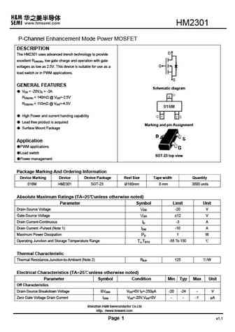
HM2301 P-Channel Enhancement Mode Power MOSFET DESCRIPTION D The HM2301 uses advanced trench technology to provide excellent RDS(ON), low gate charge and operation with gate G voltages as low as 2.5V. This device is suitable for use as a load switch or in PWM applications. S GENERAL FEATURES Schematic diagram VDS = -20V,ID = -3A RDS(ON)
9.14. Size:1133K cn hmsemi
hm2301bkr.pdf 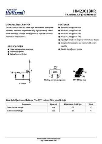
HM2301BKR P-Channel 20V (D-S) MOSFET GENERAL DESCRIPTION FEATURES The HM2301BKR is the P-Channel logic enhancement mode power RDS(ON)= 0.48 @VGS=-4.5V field effect transistors are produced using high cell density, DMOS RDS(ON)= 0.67 @VGS=-2.5V trench technology. This high density process is especially tailored to RDS(ON)= 0.95 @VGS=-1.8V minimize on-state resist
9.15. Size:418K cn hmsemi
hm2302.pdf 
HM2302 N-Channel Enhancement Mode Power MOSFET DESCRIPTION D The HM2302 uses advanced trench technology to provide excellent RDS(ON), low gate charge and operation with gate G voltages as low as 2.5V. This device is suitable for use as a Battery protection or in other Switching application. S Schematic diagram GENERAL FEATURES VDS = 20V,ID = 2.9A D 3 RDS(ON)
9.16. Size:644K cn hmsemi
hm2300d.pdf 
HM2300D N-Channel Enhancement Mode Power MOSFET Description D The HM2300D uses advanced trench technology to provide excellent RDS(ON), low gate charge and operation with gate G voltages as low as 2.5V. This device is suitable for use as a battery protection or in other switching application. S Schematic diagram General Features VDS = 20V,ID = 6.0A RDS(ON)
9.17. Size:567K cn hmsemi
hm2300b.pdf 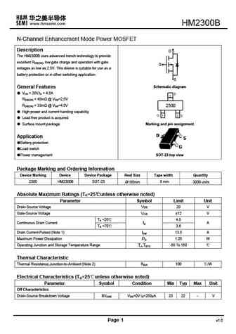
HM2300B N-Channel Enhancement Mode Power MOSFET Description D The HM2300B uses advanced trench technology to provide excellent RDS(ON), low gate charge and operation with gate G voltages as low as 2.5V. This device is suitable for use as a battery protection or in other switching application. S Schematic diagram General Features VDS = 20V,ID = 4.5A RDS(ON)
9.18. Size:194K cn hmsemi
hm2302bwsr.pdf 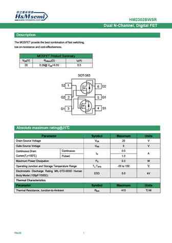
Description The MOSFET provide the best combination of fast switching, low on-resistance and cost-effectiveness. MOSFET Product Summary VDS(V) RDS(on)( ) ID(A) 20 0.29@ VGS=4.5V 0.5 SOT-563 S2 1 D2 6 G2 2 G1 5 4 S1 3 D1 Absolute maximum rating@25 Parameter Symbol Maximum Units Drain-Source Voltage
9.19. Size:1387K cn hmsemi
hm2301bsr.pdf 
HM2301BSR P-Channel 20V (D-S) MOSFET GENERAL DESCRIPTION FEATURES The HM2301BSR is the P-Channel logic enhancement mode power RDS(ON)= 0.48 @VGS=-4.5V field effect transistors are produced using high cell density, DMOS RDS(ON)= 0.67 @VGS=-2.5V trench technology. This high density process is especially tailored to RDS(ON)= 0.95 @VGS=-1.8V minimize on-state resist
9.20. Size:484K cn hmsemi
hm2302kr.pdf 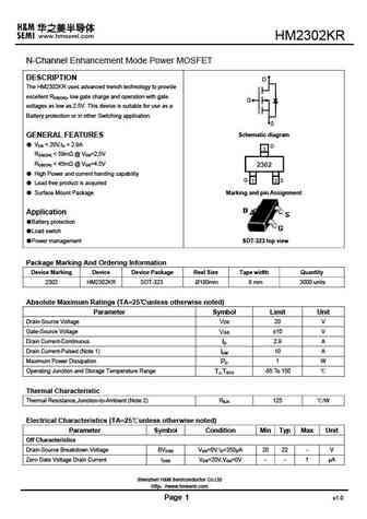
HM2302KR N-Channel Enhancement Mode Power MOSFET DESCRIPTION D The HM2302KR uses advanced trench technology to provide excellent RDS(ON), low gate charge and operation with gate G voltages as low as 2.5V. This device is suitable for use as a Battery protection or in other Switching application. S Schematic diagram GENERAL FEATURES VDS = 20V,ID = 2.9A D 3 RDS(ON)
9.21. Size:803K cn hmsemi
hm2301b.pdf 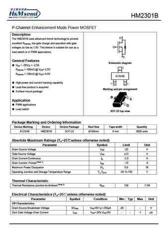
HM2301B P-Channel Enhancement Mode Power MOSFET Description D The HM2301B uses advanced trench technology to provide excellent RDS(ON), low gate charge and operation with gate G voltages as low as 1.8V. This device is suitable for use as a load switch or in PWM applications. S General Features Schematic diagram VDS = -20V,ID = -2.5A RDS(ON)
9.22. Size:1022K cn hmsemi
hm2309b.pdf 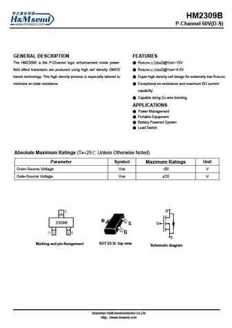
HM2309B P-Channel 60V(D-S) GENERAL DESCRIPTION FEATURES RDS(ON) 188m @VGS=-10V The HM2309B is the P-Channel logic enhancement mode power RDS(ON) 266m @VGS=-4.5V field effect transistors are produced using high cell density, DMOS Super high density cell design for extremely low RDS(ON) trench technology. This high density process is especially tailored to
9.23. Size:880K cn hmsemi
hm2302f.pdf 
HM2302F N-Channel Enhancement Mode Power MOSFET Description The HM2302F uses advanced trench technology to provide excellent RDS(ON), low gate charge and operation with gate voltages as low as 2.5V. This device is suitable for use as a Battery protection or in other Switching application. Schematic diagram General Features VDS = 20V,ID = 2.8A RDS(ON)
9.24. Size:1067K cn hmsemi
hm2300pr.pdf 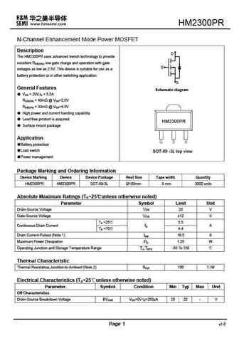
HM2300PR N-Channel Enhancement Mode Power MOSFET Description D The HM2300PR uses advanced trench technology to provide excellent RDS(ON), low gate charge and operation with gate G voltages as low as 2.5V. This device is suitable for use as a battery protection or in other switching application. S General Features Schematic diagram VDS = 20V,ID = 5.5A RDS(ON)
9.25. Size:678K cn hmsemi
hm2300c.pdf 
HM2300C N-Channel Enhancement Mode Power MOSFET Description D The HM2300C uses advanced trench technology to provide excellent RDS(ON), low gate charge and operation with gate G voltages as low as 2.5V. This device is suitable for use as a battery protection or in other switching application. S Schematic diagram General Features VDS = 20V,ID = 6.0A RDS(ON)
9.26. Size:413K cn hmsemi
hm2309d.pdf 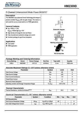
P-Channel Enhancement Mode Power MOSFET Description The HM2309D uses advanced trench technology and design to provide excellent RDS(ON) with low gate charge .This device is well suited for use as a load switch or in PWM applications. General Features VDS =-60V,ID =-1.6A Schematic diagram RDS(ON)
9.27. Size:727K cn hmsemi
hm2301e.pdf 
HM2301E P-Channel Trench Power MOSFET General Description The HM2301E uses advanced trench technology to provide excellent R , low gate charge and operation with gate DS(ON) voltages as low as -2.5V. This device is suitable for use as a battery protection or in other switching application. Features Schematic Diagram VDS = -12V,ID =-2.0A R
9.28. Size:773K cn hmsemi
hm2302dr.pdf 
GENERAL DESCRIPTION FEATURES The HM2302DR is the N-Channel logic enhancement mode power RDS(ON)= 270 m @VGS=4.5V field effect transistors are produced using high cell density, DMOS RDS(ON)= 330 m @VGS=2.5V trench technology. This high density process is especially tailored to RDS(ON)= 450 m @VGS=1.8V minimize on-state resistan
9.29. Size:273K cn hmsemi
hm2301bjr.pdf 
HM2301BJR P-Channel MOSFET Description The MOSFET provide the best combination of fast switching, D 3 low on-resistance and cost-effectiveness. MOSFET Product Summary V (V) R ( ) I (mA) DS DS(on) D 0.45@ V =-4.5V GS G 1 -20 0.62@ VGS=-2.5V -800 0.86@ V =-1.8V GS S 2 Absolute maximum rating@25 Parameter Symbol Value Units Drain-Source Voltage
9.30. Size:742K cn hmsemi
hm2305d.pdf 
HM2305D P-Channel Enhancement Mode Power MOSFET Description D The HM2305D uses advanced trench technology to provide excellent RDS(ON), low gate charge and operation with gate G voltages as low as 2.5V. This device is suitable for use as a S load switch or in PWM applications. Schematic diagram General Features VDS = -20V,ID = -8.0A RDS(ON)
9.32. Size:608K cn hmsemi
hm2301dr.pdf 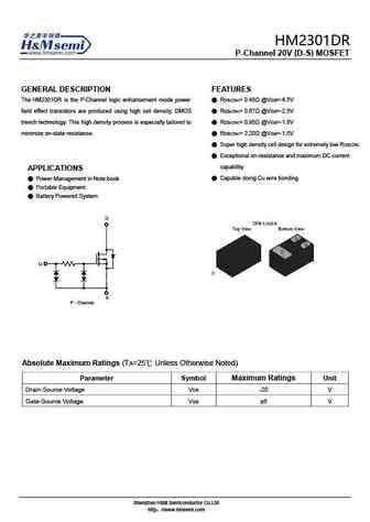
H P-Channel 20V (D-S) MOSFET GENERAL DESCRIPTION FEATURES The is the P-Channel logic enhancement mode power RDS(ON)= 0.48 @VGS=-4.5V field effect transistors are produced using high cell density, DMOS RDS(ON)= 0.67 @VGS=-2.5V trench technology. This high density process is especially tailored to RDS(ON)= 0.95 @VGS=-1.8V minimize on-state resistan
9.33. Size:704K cn hmsemi
hm2301d.pdf 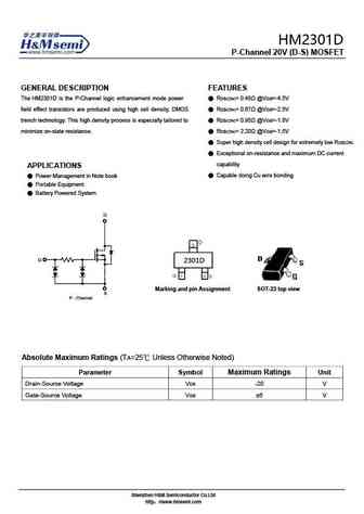
H P-Channel 20V (D-S) MOSFET GENERAL DESCRIPTION FEATURES The is the P-Channel logic enhancement mode power RDS(ON)= 0.48 @VGS=-4.5V field effect transistors are produced using high cell density, DMOS RDS(ON)= 0.67 @VGS=-2.5V trench technology. This high density process is especially tailored to RDS(ON)= 0.95 @VGS=-1.8V minimize on-state resistance
9.34. Size:593K cn hmsemi
hm2309apr.pdf 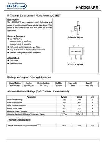
HM2309APR P-Channel Enhancement Mode Power MOSFET Description The HM2309APR uses advanced trench technology and design to provide excellent RDS(ON) with low gate charge .This device is well suited for use as a load switch or in PWM applications. General Features Schematic diagram VDS =-60V,ID =-5A RDS(ON)
9.35. Size:541K cn hmsemi
hm2309c.pdf 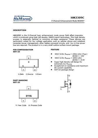
P Channel Enhancement Mode MOSFET DESCRIPTION HM2309C is the P-Channel logic enhancement mode power field effect transistor which is produced using high cell density, DMOS trench technology. This high density process is especially tailored to minimize on-state resistance. These devices are particularly suited for low voltage application such as cellular phone and notebook
9.36. Size:369K cn hmsemi
hm2302bwkr.pdf 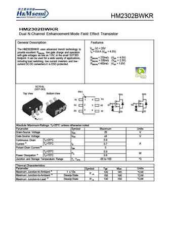
HM2302BWKR Dual N-Channel Enhancement Mode Field Effect Transistor General Description Features The HM2302BWKR uses advanced trench technology to VDS (V) = 20V ID = 0.9 A (VGS = 4.5V) excellent RDS(ON), low gate charge and operation voltages as low as 1.8V, in the small SOT363 RDS(ON)
9.37. Size:1397K cn hmsemi
hm2302bjr.pdf 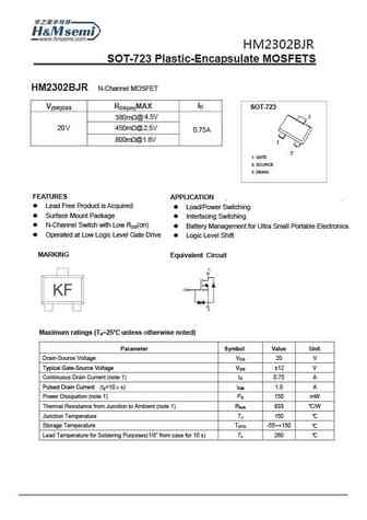
J HM2302BJR SOT-723 Plastic-Encapsulate MOSFETS HM2302BJR N-Channel MOSFET ID V(BR)DSS RDS(on)MAX SOT-723 380m @ 4.5V 20V 450m @2.5V 0.75A 800m @1.8V 1. GATE 2. SOURCE 3. DRAIN FEATURES APPLICATION Lead Free Product is Acquired Load/Power Switching Surface Mount Package Interfacing Switching N-Channel Switch with Low RDS(on) Battery Manage
9.38. Size:977K cn hmsemi
hm2300dr.pdf 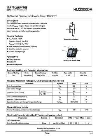
HM2300DR N-Channel Enhancement Mode Power MOSFET Description The HM2300DR uses advanced trench technology to provide D excellent RDS(ON), low gate charge and operation with gate voltages as low as 2.5V. This device is suitable for use as a G battery protection or in other switching application. S General Features VDS = 20V,ID = 8.0A Schematic diagram RDS(ON)
9.39. Size:1451K cn hmsemi
hm2301kr.pdf 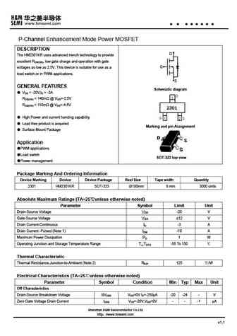
HM2301KR P-Channel Enhancement Mode Power MOSFET DESCRIPTION D The HM2301KR uses advanced trench technology to provide excellent RDS(ON), low gate charge and operation with gate G voltages as low as 2.5V. This device is suitable for use as a load switch or in PWM applications. S GENERAL FEATURES Schematic diagram VDS = -20V,ID = -3A RDS(ON)
9.40. Size:482K cn hmsemi
hm2305pr.pdf 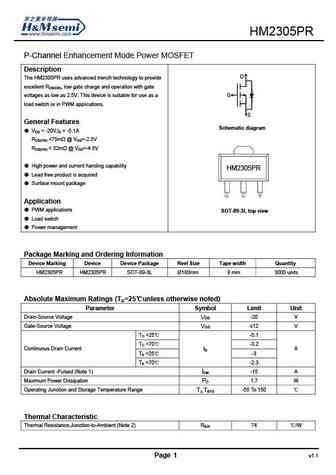
HM2305PR P-Channel Enhancement Mode Power MOSFET Description D The HM2305PR uses advanced trench technology to provide excellent RDS(ON), low gate charge and operation with gate voltages as low as 2.5V. This device is suitable for use as a G load switch or in PWM applications. S General Features Schematic diagram VDS = -20V,ID = - .1A RDS(ON)
9.41. Size:648K cn hmsemi
hm2302b.pdf 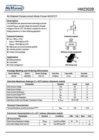
HM2302B N-Channel Enhancement Mode Power MOSFET Description The HM2302B uses advanced trench technology to provide excellent RDS(ON), low gate charge and operation with gate voltages as low as 2.5V. This device is suitable for use as a Battery protection or in other Switching application. Schematic diagram General Features VDS = 20V,ID = 2.5A RDS(ON)
9.42. Size:806K cn hmsemi
hm2302e.pdf 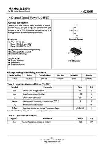
HM2302E N-Channel Trench Power MOSFET General Description The HM2302E uses advanced trench technology to provide excellent R , low gate charge and operation with gate DS(ON) voltages as low as 2.5V. This device is suitable for use as a battery protection or in other switching application. Schematic Diagram Features VDS = 15V,ID =2.0A R
9.43. Size:1017K cn hmsemi
hm2302d.pdf 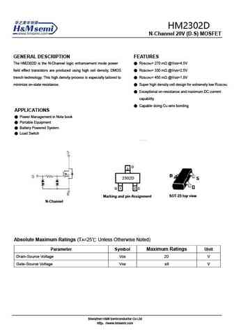
GENERAL DESCRIPTION FEATURES The HM2302D is the N-Channel logic enhancement mode power RDS(ON)= 270 m @VGS=4.5V field effect transistors are produced using high cell density, DMOS RDS(ON)= 330 m @VGS=2.5V trench technology. This high density process is especially tailored to RDS(ON)= 450 m @VGS=1.8V minimize on-state resistance
9.44. Size:465K cn hmsemi
hm2309al.pdf 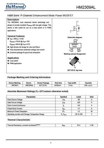
HM2309AL H&M Semi P-Channel Enhancement Mode Power MOSFET Description The HM2309AL uses advanced trench technology and design to provide excellent RDS(ON) with low gate charge .This device is well suited for use as a load switch or in PWM applications. General Features Schematic diagram VDS =-60V,ID =-4.6A RDS(ON)
9.45. Size:977K cn hmsemi
hm2301f.pdf 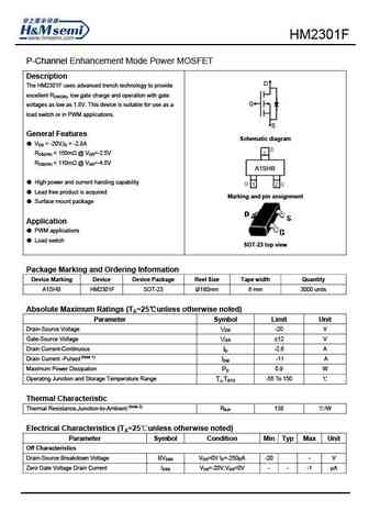
HM2301F P-Channel Enhancement Mode Power MOSFET Description D The HM2301F uses advanced trench technology to provide excellent RDS(ON), low gate charge and operation with gate G voltages as low as 1.8V. This device is suitable for use as a load switch or in PWM applications. S General Features Schematic diagram VDS = -20V,ID = -2.8A RDS(ON)
9.47. Size:553K cn hmsemi
hm2300.pdf 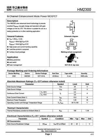
HM2300 N-Channel Enhancement Mode Power MOSFET Description D The HM2300 uses advanced trench technology to provide excellent RDS(ON), low gate charge and operation with gate G voltages as low as 2.5V. This device is suitable for use as a battery protection or in other switching application. S Schematic diagram General Features VDS = 20V,ID = 4.5A RDS(ON)
9.48. Size:473K cn hmsemi
hm2305.pdf 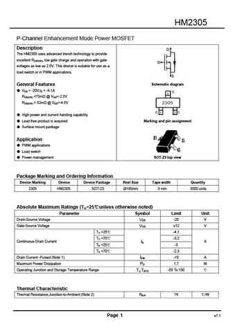
P-Channel Enhancement Mode Power MOSFET Description D The uses advanced trench technology to provide excellent RDS(ON), low gate charge and operation with gate G voltages as low as 2.5V. This device is suitable for use as a load switch or in PWM applications. S Schematic diagram General Features VDS = -20V,ID = -4.1A RDS(ON)
Другие MOSFET... HM2302D
, HM2302DR
, HM2302E
, HM2302F
, HM2302KR
, HM2305
, HM2305B
, HM2305D
, IRFP460
, HM2309
, HM2309AL
, HM2309APR
, HM2309B
, HM2309C
, HM2309D
, HM2309DR
, HM2310B
.
History: FA38SA50LCP
| AT10N65S