3N100 datasheet, аналоги, основные параметры
Наименование производителя: 3N100 📄📄
Тип материала: Si
Полярность: PNP
Предельные значения
Максимальная рассеиваемая мощность (Pc): 0.3 W
Макcимально допустимое напряжение коллектор-эмиттер (Uce): 20 V
Макcимальный постоянный ток коллектора (Ic): 0.05 A
Предельная температура PN-перехода (Tj): 175 °C
Электрические характеристики
Граничная частота коэффициента передачи тока (ft): 3 MHz
Корпус транзистора: TO72
📄📄 Копировать
Аналоги (замена) для 3N100
- подборⓘ биполярного транзистора по параметрам
3N100 даташит
0.1. Size:262K motorola
mtb3n100erev2x.pdf 
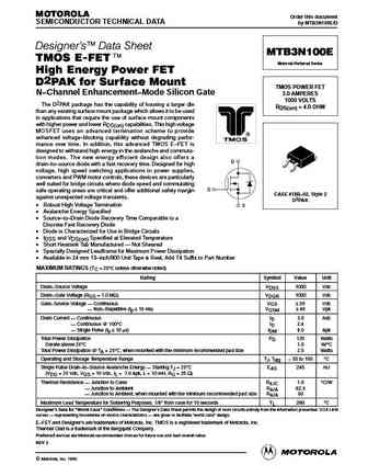
MOTOROLA Order this document SEMICONDUCTOR TECHNICAL DATA by MTB3N100E/D Designer's Data Sheet MTB3N100E TMOS E-FET. Motorola Preferred Device High Energy Power FET D2PAK for Surface Mount TMOS POWER FET N Channel Enhancement Mode Silicon Gate 3.0 AMPERES 1000 VOLTS The D2PAK package has the capability of housing a larger die RDS(on) = 4.0 OHM than any existing surface
0.2. Size:179K motorola
mtp3n100e.pdf 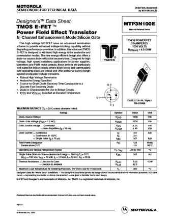
MOTOROLA Order this document SEMICONDUCTOR TECHNICAL DATA by MTP3N100E/D Designer's Data Sheet MTP3N100E TMOS E-FET. Motorola Preferred Device Power Field Effect Transistor N Channel Enhancement Mode Silicon Gate TMOS POWER FET This high voltage MOSFET uses an advanced termination 3.0 AMPERES scheme to provide enhanced voltage blocking capability without 1000 VOLTS de
0.3. Size:226K motorola
mtb3n100e.pdf 
MOTOROLA Order this document SEMICONDUCTOR TECHNICAL DATA by MTB3N100E/D Designer's Data Sheet MTB3N100E TMOS E-FET. Motorola Preferred Device High Energy Power FET D2PAK for Surface Mount TMOS POWER FET N Channel Enhancement Mode Silicon Gate 3.0 AMPERES 1000 VOLTS The D2PAK package has the capability of housing a larger die RDS(on) = 4.0 OHM than any existing surface
0.5. Size:206K motorola
mtp3n100e-.pdf 
MOTOROLA Order this document SEMICONDUCTOR TECHNICAL DATA by MTP3N100E/D Designer's Data Sheet MTP3N100E TMOS E-FET. Motorola Preferred Device Power Field Effect Transistor N Channel Enhancement Mode Silicon Gate TMOS POWER FET This high voltage MOSFET uses an advanced termination 3.0 AMPERES scheme to provide enhanced voltage blocking capability without 1000 VOLTS de
0.7. Size:366K st
stp3n100.pdf 
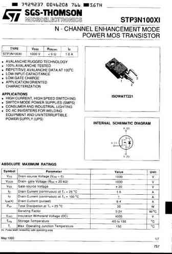
STP3N100 STP3N100FI N - CHANNEL ENHANCEMENT MODE POWER MOS TRANSISTOR TYPE VDSS RDS(on) ID STP3N100 1000 V
0.8. Size:184K ixys
ixta3n100d2hv.pdf 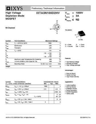
Preliminary Technical Information High Voltage VDSX = 1000V IXTA3N100D2HV Depletion Mode ID(on) > 3A MOSFET RDS(on) 6 D N-Channel G TO-263HV S G S D (Tab) Symbol Test Conditions Maximum Ratings VDSX TJ = 25 C to 150 C 1000 V G = Gate D = Drain VGSX Continuous 20 V S = Source Tab = Drain VGSM Transient 30 V PD TC = 25 C 1
0.9. Size:150K ixys
ixta3n100p ixth3n100p ixtp3n100p.pdf 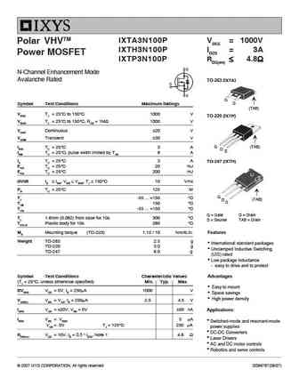
IXTA3N100P VDSS = 1000V Polar VHVTM IXTH3N100P ID25 = 3A Power MOSFET IXTP3N100P RDS(on) 4.8 N-Channel Enhancement Mode Avalanche Rated TO-263 (IXTA) G S Symbol Test Conditions Maximum Ratings (TAB) VDSS TJ = 25 C to 150 C 1000 V TO-220 (IXTP) VDGR TJ = 25 C to 150 C, RGS = 1M 1000 V VGSS Continuous 20 V VGSM Transient 30 V (TAB)
0.10. Size:383K aosemi
aot3n100 aotf3n100.pdf 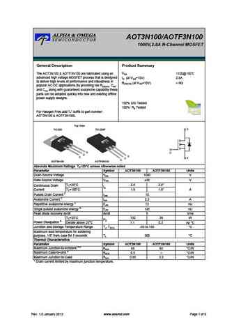
AOT3N100/AOTF3N100 1000V,2.8A N-Channel MOSFET General Description Product Summary VDS 1100@150 The AOT3N100 & AOTF3N100 are fabricated using an advanced high voltage MOSFET process that is designed ID (at VGS=10V) 2.8A to deliver high levels of performance and robustness in RDS(ON) (at VGS=10V)
0.11. Size:329K aosemi
aot3n100.pdf 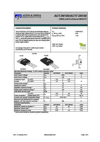
AOT3N100/AOTF3N100 1000V,2.8A N-Channel MOSFET General Description Product Summary VDS 1100@150 The AOT3N100 & AOTF3N100 are fabricated using an advanced high voltage MOSFET process that is designed ID (at VGS=10V) 2.8A to deliver high levels of performance and robustness in RDS(ON) (at VGS=10V)
0.12. Size:329K aosemi
aotf3n100.pdf 
AOT3N100/AOTF3N100 1000V,2.8A N-Channel MOSFET General Description Product Summary VDS 1100@150 The AOT3N100 & AOTF3N100 are fabricated using an advanced high voltage MOSFET process that is designed ID (at VGS=10V) 2.8A to deliver high levels of performance and robustness in RDS(ON) (at VGS=10V)
0.13. Size:1014K belling
bl3n100e-p bl3n100e-a bl3n100e-u bl3n100e-d.pdf 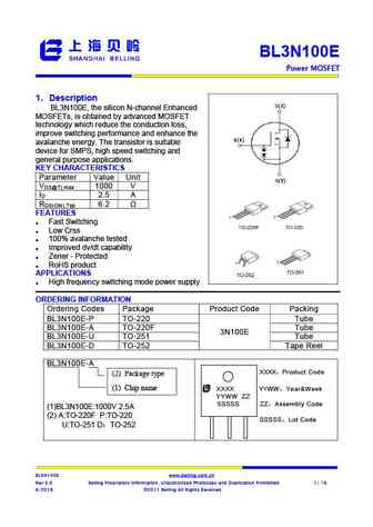
BL3N100E Power MOSFET 1 Description Step-Down Converter BL3N100E, the silicon N-channel Enhanced , MOSFETs, is obtained by advanced MOSFET technology which reduce the conduction loss, improve switching performance and enhance the avalanche energy. The transistor is suitable device for SMPS, high speed switching and general purpose applications. KEY CHARACTERISTICS P
0.14. Size:660K belling
bl3n100-p bl3n100-a bl3n100-u bl3n100-d.pdf 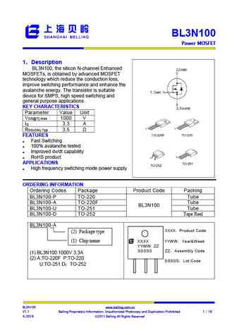
BL3N100 Power MOSFET Power MOSFET Power MOSFET Power MOSFET 1 Description BL3N100, the silicon N-channel Enhanced MOSFETs, is obtained by advanced MOSFET technology which reduce the conduction loss, improve switching performance and enhance the avalanche energy. The transistor is suitable device for SMPS, high speed switching and general purpose applicatio
0.15. Size:410K chenmko
t03n100gp.pdf 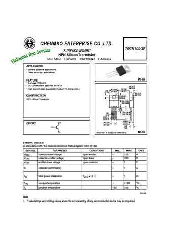
CHENMKO ENTERPRISE CO.,LTD T03N100GP SURFACE MOUNT NPN Silicon Transistor VOLTAGE 100Volts CURRENT 3 Ampere APPLICATION * General purpose applications. * Other switching applications. TO-220 FEATURE * Package. (TO-220) * DC Current Gain Specified to Ic=3A ( ) .187 4.7 ( ) .148 3.8 ( ) .153 3.9 * High Current Gain-Bandwidth Product fT=3MHz (Min.) .413 10.5 ( ) .108 ( )
0.16. Size:429K convert
cs3n100f cs3n100p.pdf 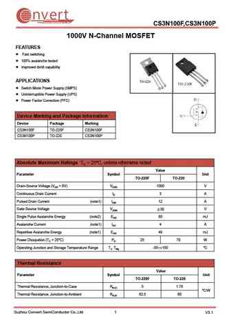
nvert Suzhou Convert Semiconductor Co ., Ltd. CS3N100F,CS3N100P 1000V N-Channel MOSFET FEATURES Fast switching 100% avalanche tested Improved dv/dt capability APPLICATIONS Switch Mode Power Supply (SMPS) Uninterruptible Power Supply (UPS) Power Factor Correction (PFC) Device Marking and Package Information Device Package Marking CS3N100F TO-220F CS3N100F C
0.17. Size:397K convert
cs3n100f.pdf 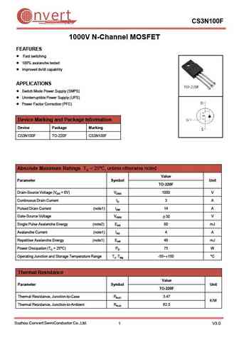
nvert Suzhou Convert Semiconductor Co ., Ltd. CS3N100F 1000V N-Channel MOSFET FEATURES Fast switching 100% avalanche tested Improved dv/dt capability APPLICATIONS Switch Mode Power Supply (SMPS) Uninterruptible Power Supply (UPS) Power Factor Correction (PFC) Device Marking and Package Information Device Package Marking CS3N100F TO-220F CS3N100F Absolute Ma
0.18. Size:2226K cn scilicon
sfp043n100c3 sfb040n100c3.pdf 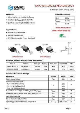
SFP043N100C3,SFB040N100C3 N-MOSFET 100V, 3.4m , 120A Features Product Summary Extremely low on-resistance RDS(on) VDS 100V Excellent QgxRDS(on) product(FOM) RDS(on) 3.4m Qualified according to JEDEC criteria ID 120A 100% DVDS Tested Applications 100% Avalanche Tested Motor control and drive Battery management UPS (Uninterrupible Power Supplies) SFP
0.19. Size:646K cn scilicon
sfb053n100c3.pdf 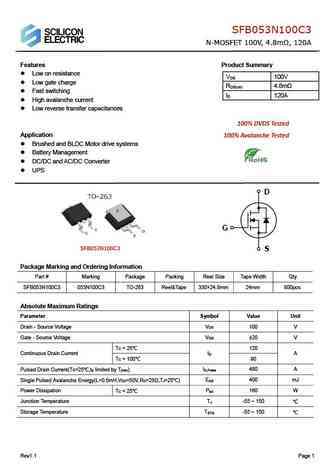
SFB053N100C3 N-MOSFET 100V, 4.8m , 120A Features Product Summary Low on resistance V 100V DS Low gate charge R 4.8m DS(on) Fast switching I 120A D High avalanche current Low reverse transfer capacitances 100% DVDS Tested Application 100% Avalanche Tested Brushed and BLDC Motor drive systems Battery Management DC/DC and AC/DC Converte
0.20. Size:261K inchange semiconductor
aot3n100.pdf 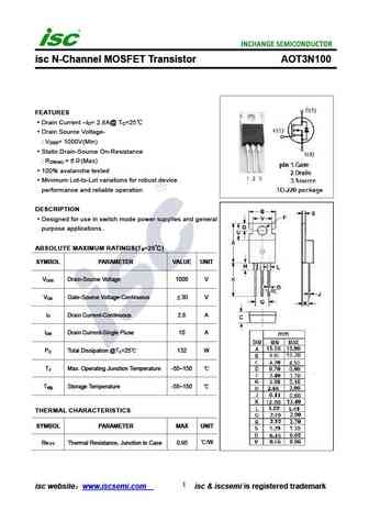
isc N-Channel MOSFET Transistor AOT3N100 FEATURES Drain Current I = 2.8A@ T =25 D C Drain Source Voltage- V = 1000V(Min) DSS Static Drain-Source On-Resistance R = 6 (Max) DS(on) 100% avalanche tested Minimum Lot-to-Lot variations for robust device performance and reliable operation DESCRIPTION Designed for use in switch mode power supplies and general purpo
0.21. Size:252K inchange semiconductor
aotf3n100.pdf 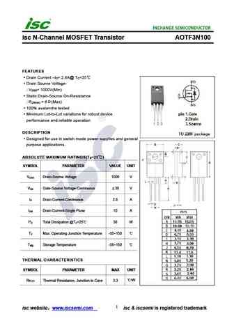
isc N-Channel MOSFET Transistor AOTF3N100 FEATURES Drain Current I = 2.8A@ T =25 D C Drain Source Voltage- V = 1000V(Min) DSS Static Drain-Source On-Resistance R = 6 (Max) DS(on) 100% avalanche tested Minimum Lot-to-Lot variations for robust device performance and reliable operation DESCRIPTION Designed for use in switch mode power supplies and general purp
Другие транзисторы: 30DB040D, 35DB070D, 35DB080D, 37740, 37741, 38387, 38388, 38647, S8550, 3N101, 3N102, 3N103, 3N104, 3N105, 3N106, 3N107, 3N108