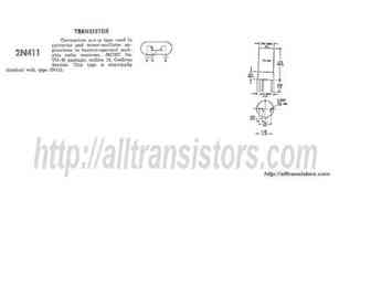
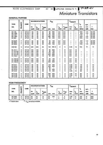
Аналоги 411. Основные параметры
Наименование производителя: 411
Тип материала: Si
Полярность: NPN
Максимальная рассеиваемая мощность (Pc): 125 W
Макcимально допустимое напряжение коллектор-база (Ucb): 300 V
Макcимально допустимое напряжение коллектор-эмиттер (Uce): 300 V
Макcимально допустимое напряжение эмиттер-база (Ueb): 5 V
Макcимальный постоянный ток коллектора (Ic): 7 A
Предельная температура PN-перехода (Tj): 150 °C
Граничная частота коэффициента передачи тока (ft): 4 MHz
Статический коэффициент передачи тока (hfe): 10
Корпус транзистора: TO3
Аналоги (замена) для 411
411 даташит
hsbb4115.pdf
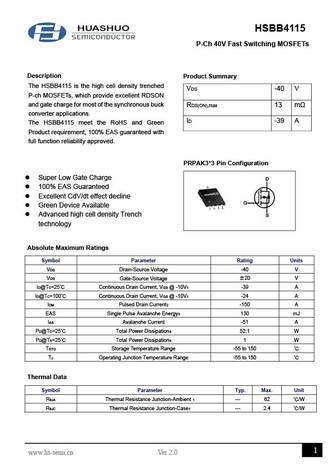
HSBB4115 P-Ch 40V Fast Switching MOSFETs Description Product Summary The HSBB4115 is the high cell density trenched VDS -40 V P-ch MOSFETs, which provide excellent RDSON and gate charge for most of the synchronous buck RDS(ON),max 13 m converter applications. ID -39 A The HSBB4115 meet the RoHS and Green Product requirement, 100% EAS guaranteed with full function relia
hsba4115.pdf
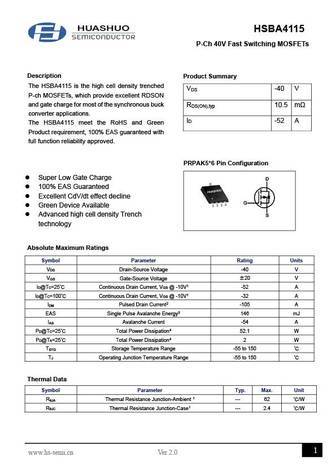
HSBA4115 P-Ch 40V Fast Switching MOSFETs Description Product Summary The HSBA4115 is the high cell density trenched V -40 V DS P-ch MOSFETs, which provide excellent RDSON and gate charge for most of the synchronous buck R 10.5 m DS(ON),typ converter applications. I -52 A D The HSBA4115 meet the RoHS and Green Product requirement, 100% EAS guaranteed with full functi
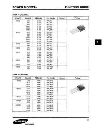
aon6411.pdf
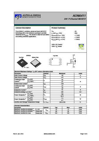
AON6411 20V P-Channel MOSFET General Description Product Summary VDS -20 The AON6411 combines advanced trench MOSFET technology with a low resistance package to provide ID (at VGS= -10V) -85A extremely low RDS(ON). This device is ideal for load switch RDS(ON) (at VGS= -10V)
irfs4115-7ppbf.pdf
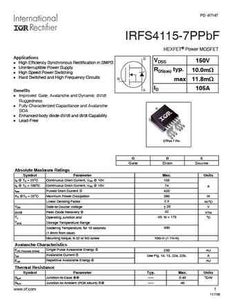
PD -97147 IRFS4115-7PPbF HEXFET Power MOSFET Applications D VDSS 150V l High Efficiency Synchronous Rectification in SMPS l Uninterruptible Power Supply RDS(on) typ. 10.0m l High Speed Power Switching l Hard Switched and High Frequency Circuits G max. 11.8m ID 105A S Benefits l Improved Gate, Avalanche and Dynamic dV/dt Ruggedness l Fully Characterized Capacitance
irfb4115gpbf.pdf
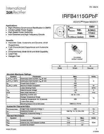
PD - 96216 IRFB4115GPbF HEXFET Power MOSFET Applications D VDSS 150V l High Efficiency Synchronous Rectification in SMPS l Uninterruptible Power Supply RDS(on) typ. 9.3m l High Speed Power Switching G max. 11m l Hard Switched and High Frequency Circuits ID (Silicon Limited) 104A S Benefits l Improved Gate, Avalanche and Dynamic dV/dt Ruggedness D l Fully Characterize
irfb4115pbf.pdf
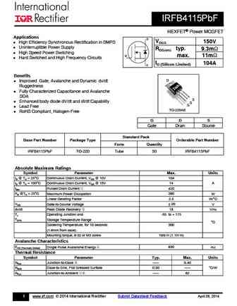
IRFB4115PbF HEXFET Power MOSFET Applications D VDSS 150V l High Efficiency Synchronous Rectification in SMPS l Uninterruptible Power Supply RDS(on) typ. 9.3m l High Speed Power Switching G max. 11m l Hard Switched and High Frequency Circuits ID (Silicon Limited) 104A S Benefits D l Improved Gate, Avalanche and Dynamic dv/dt Ruggedness l Fully Characterized Capacita
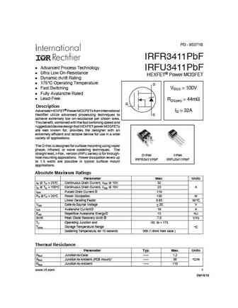
irfr3411pbf irfu3411pbf.pdf
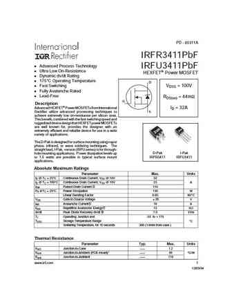
PD - 95371A IRFR3411PbF l Advanced Process Technology IRFU3411PbF l Ultra Low On-Resistance HEXFET Power MOSFET l Dynamic dv/dt Rating l 175 C Operating Temperature D l Fast Switching VDSS = 100V l Fully Avalanche Rated l Lead-Free RDS(on) = 44m G Description Advanced HEXFET Power MOSFETs from International ID = 32A S Rectifier utilize advanced processing techniques to
irfs4115pbf irfsl4115pbf.pdf
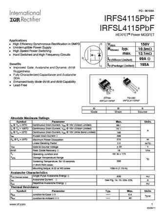
PD - 96198A IRFS4115PbF IRFSL4115PbF HEXFET Power MOSFET Applications D l High Efficiency Synchronous Rectification in SMPS VDSS 150V l Uninterruptible Power Supply RDS(on) typ. 10.3m l High Speed Power Switching max. 12.1m l Hard Switched and High Frequency Circuits G ID (Silicon Limited) 99A Benefits ID (Package Limited) 195A S l Improved Gate, Avalanche and Dynamic
irfr3411pbf.pdf
PD - 95371B IRFR3411PbF l Advanced Process Technology IRFU3411PbF l Ultra Low On-Resistance HEXFET Power MOSFET l Dynamic dv/dt Rating l 175 C Operating Temperature D l Fast Switching VDSS = 100V l Fully Avalanche Rated l Lead-Free RDS(on) = 44m G Description Advanced HEXFET Power MOSFETs from International ID = 32A S Rectifier utilize advanced processing techniques to
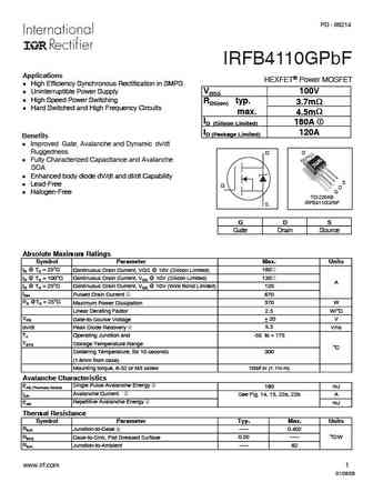
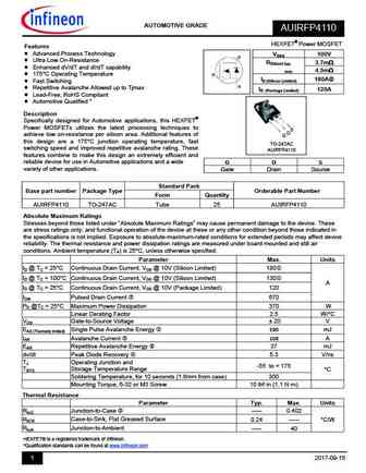
irfp4110pbf.pdf
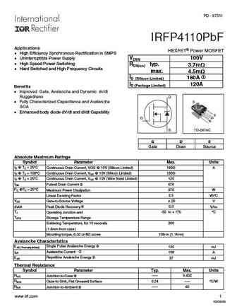
PD - 97311 IRFP4110PbF Applications HEXFET Power MOSFET l High Efficiency Synchronous Rectification in SMPS l Uninterruptible Power Supply VDSS 100V l High Speed Power Switching RDS(on) typ. 3.7m l Hard Switched and High Frequency Circuits max. 4.5m ID (Silicon Limited) 180A c ID (Package Limited) 120A Benefits l Improved Gate, Avalanche and Dynamic dv/dt Ruggedness D l
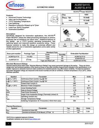
auirfsl4115.pdf
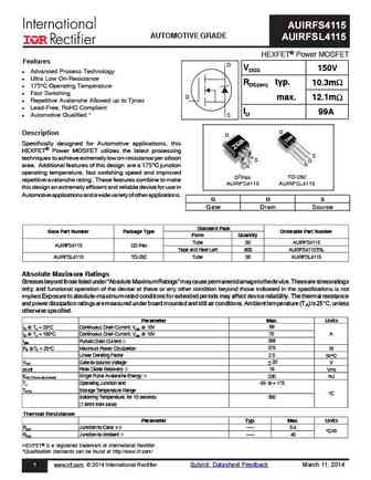
AUIRFS4115 AUTOMOTIVE GRADE AUIRFSL4115 HEXFET Power MOSFET Features D VDSS 150V l Advanced Process Technology l Ultra Low On-Resistance RDS(on) typ. 10.3m l 175 C Operating Temperature l Fast Switching G max. 12.1m l Repetitive Avalanche Allowed up to Tjmax l Lead-Free, RoHS Compliant ID 99A l Automotive Qualified * S D Description D Specifically designed for A
irfi4110gpbf.pdf
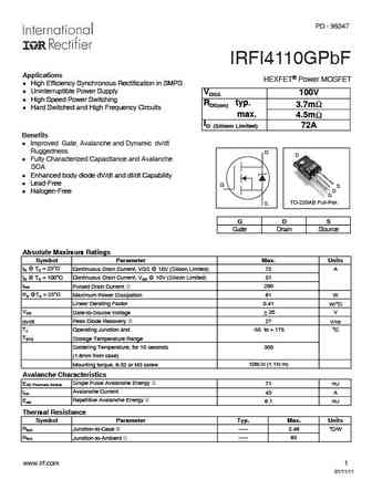
PD - 96347 IRFI4110GPbF Applications HEXFET Power MOSFET l High Efficiency Synchronous Rectification in SMPS l Uninterruptible Power Supply VDSS 100V l High Speed Power Switching RDS(on) typ. 3.7m l Hard Switched and High Frequency Circuits max. 4.5m ID (Silicon Limited) 72A Benefits l Improved Gate, Avalanche and Dynamic dv/dt Ruggedness D D l Fully Characterized
irfr3411.pdf
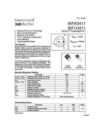
PD - 94393 IRFR3411 IRFU3411 Advanced Process Technology HEXFET Power MOSFET Ultra Low On-Resistance Dynamic dv/dt Rating D VDSS = 100V 175 C Operating Temperature Fast Switching Fully Avalanche Rated RDS(on) = 44m G Description Advanced HEXFET Power MOSFETs from International ID = 32A S Rectifier utilize advanced processing techniques to achieve extremely low on-
irfb4110gpbf.pdf
PD - 96214 IRFB4110GPbF Applications HEXFET Power MOSFET l High Efficiency Synchronous Rectification in SMPS l Uninterruptible Power Supply VDSS 100V l High Speed Power Switching RDS(on) typ. 3.7m l Hard Switched and High Frequency Circuits max. 4.5m ID (Silicon Limited) 180A ID (Package Limited) 120A Benefits l Improved Gate, Avalanche and Dynamic dv/dt Ruggedness D D l
irfb4110pbf.pdf
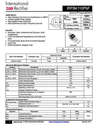
IRFB4110PbF HEXFET Power MOSFET Applications D VDSS 100V l High Efficiency Synchronous Rectification in SMPS RDS(on) typ. l Uninterruptible Power Supply 3.7m l High Speed Power Switching max. 4.5m l Hard Switched and High Frequency Circuits G ID (Silicon Limited) 180A S ID (Package Limited) 120A Benefits l Improved Gate, Avalanche and Dynamic dv/dt D Ruggedness
irfb4110qpbf.pdf
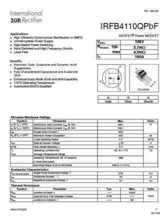
PD - 96138 IRFB4110QPbF Applications HEXFET Power MOSFET l High Efficiency Synchronous Rectification in SMPS l Uninterruptible Power Supply VDSS 100V l High Speed Power Switching RDS(on) typ. 3.7m l Hard Switched and High Frequency Circuits l Lead-Free max 4.5m ID 180A Benefits l Improved Gate, Avalanche and Dynamic dv/dt D Ruggedness D l Fully Characterized Capacitance an
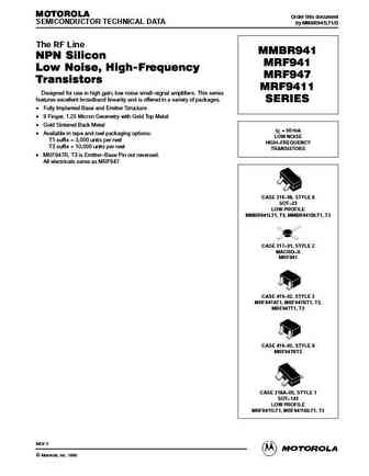
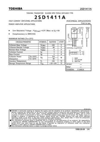
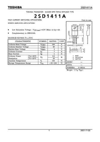
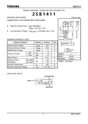
sd1411.pdf
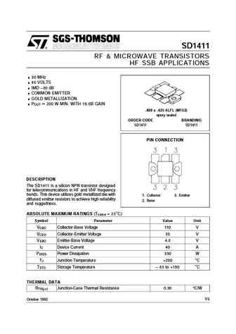
SD1411 RF & MICROWAVE TRANSISTORS HF SSB APPLICATIONS .30 MHz .40 VOLTS .IMD -30 dB .COMMON EMITTER .GOLD METALLIZATION .P 200 W MIN. WITH 16 dB GAIN = OUT .400 x .425 6LFL (M153) epoxy sealed ORDER CODE BRANDING SD1411 SD1411 PIN CONNECTION DESCRIPTION The SD1411 is a silicon NPN transistor designed for telecommunications in HF and VHF frequency bands. This device utilizes g
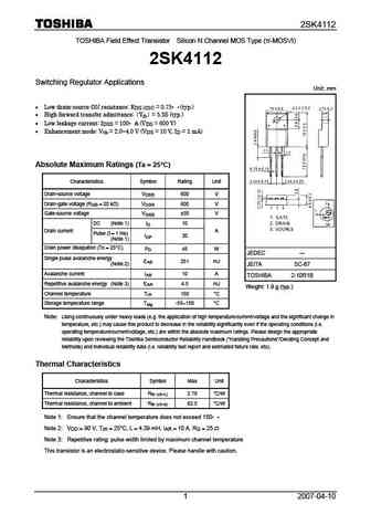
2sk4111.pdf
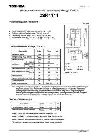
2SK4111 TOSHIBA Field Effect Transistor Silicon N Channel MOS Type ( -MOSVI) 2SK4111 Switching Regulator Applications Unit mm Low drain-source ON resistance RDS (ON) = 0.54 (typ.) High forward transfer admittance Yfs = 8.5S (typ.) Low leakage current IDSS = 100 A (max) (VDS = 600 V) Enhancement mode Vth = 2.0 to 4.0 V (VDS = 10 V, ID = 1 mA) Absolu
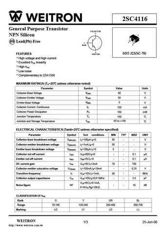
ttc4116fu.pdf
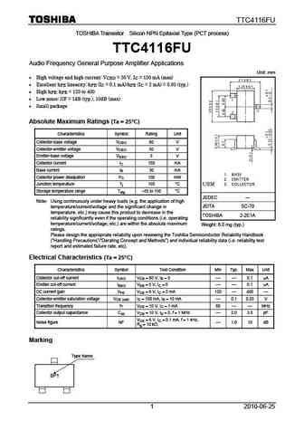
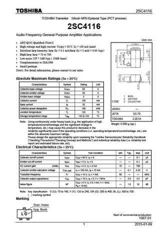
TTC4116FU TOSHIBA Transistor Silicon NPN Epitaxial Type (PCT process) TTC4116FU Audio Frequency General Purpose Amplifier Applications Unit mm High voltage and high current VCEO = 50 V, IC = 150 mA (max) Excellent hFE linearity hFE (IC = 0.1 mA)/hFE (IC = 2 mA) = 0.95 (typ.) High hFE hFE = 120 to 400 Low noise NF = 1dB (typ.), 10dB (max) Small package
2sk4115.pdf
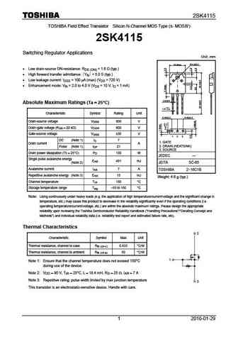
2SK4115 TOSHIBA Field Effect Transistor Silicon N-Channel MOS Type ( - MOS ) 2SK4115 Switching Regulator Applications Unit mm 3.2 0.2 15.9max. Low drain-source ON-resistance RDS (ON) = 1.6 (typ.) High forward transfer admittance Yfs = 5.0 S (typ.) Low leakage current IDSS = 100 A (max) (VDS = 720 V) Enhancement mode Vth = 2.0 to 4.0 V
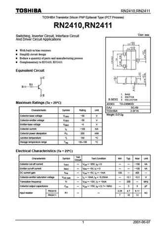
rn1410 rn1411.pdf
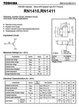
RN1410,RN1411 TOSHIBA Transistor Silicon NPN Epitaxial Type (PCT Process) RN1410,RN1411 Switching, Inverter Circuit, Interface Circuit Unit mm And Driver Circuit Applications With built-in bias resistors Simplify circuit design Reduce a quantity of parts and manufacturing process Complementary to RN2410, RN2411 Equivalent Circuit Maximum Ratings (Ta = 25 C) JED
2sc4118.pdf
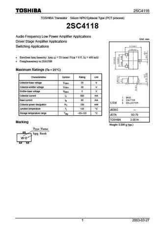
2SC4118 TOSHIBA Transistor Silicon NPN Epitaxial Type (PCT process) 2SC4118 Audio Frequency Low Power Amplifier Applications Unit mm Driver Stage Amplifier Applications Switching Applications Excellent hFE linearity hFE (2) = 25 (min) (VCE = 6 V, IC = 400 mA) Complementary to 2SA1588 Maximum Ratings (Ta = = 25 C) = = Characteristics Symbol Rating Unit Collec
mp4411.pdf
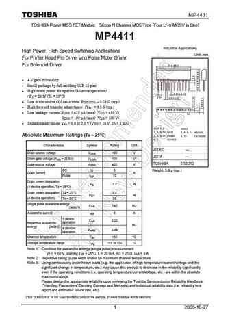
MP4411 TOSHIBA Power MOS FET Module Silicon N Channel MOS Type (Four L2- -MOSV in One) MP4411 Industrial Applications High Power, High Speed Switching Applications Unit mm For Printer Head Pin Driver and Pulse Motor Driver For Solenoid Driver 4-V gate drivability Small package by full molding (SIP 12 pin) High drain power dissipation (4-device operation) PT
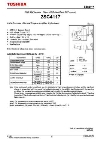
2sc4117.pdf
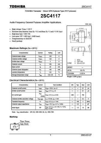
2SC4117 TOSHIBA Transistor Silicon NPN Epitaxial Type (PCT process) 2SC4117 Audio Frequency General Purpose Amplifier Applications Unit mm High voltage VCEO = 120 V Excellent h linearity h (I = 0.1 mA)/h (I = 2 mA) = 0.95 (typ.) FE FE C FE C High h h = 200 700 FE FE Low noise NF = 1dB (typ.), 10dB (max) Complementary to 2SA1587 Small package
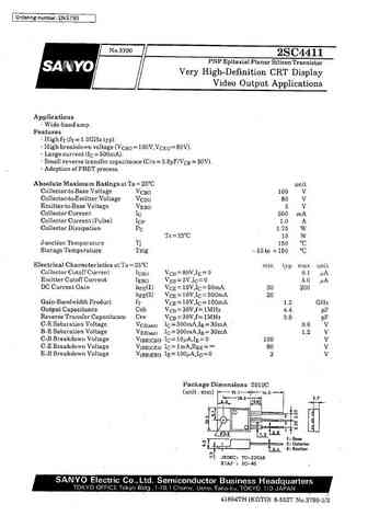
2sc5411.pdf
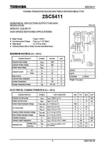
2SC5411 TOSHIBA TRANSISTOR SILICON NPN TRIPLE DIFFUSED MESA TYPE 2SC5411 HORIZONTAL DEFLECTION OUTPUT FOR HIGH Unit mm RESOLUTION DISPLAY, COLOR TV HIGH SPEED SWITCHING APPLICATIONS High Voltage VCBO = 1500 V Low Saturation Voltage V = 3 V (Max.) CE (sat) High Speed t = 0.15 s (Typ.) f Collector Metal (Fin) is Fully Covered with Mold Resin. MAXIMUM RA
rn2410-rn2411.pdf
RN2410,RN2411 TOSHIBA Transistor Silicon PNP Epitaxial Type (PCT Process) RN2410,RN2411 Unit mm Switching, Inverter Circuit, Interface Circuit And Driver Circuit Applications With built-in bias resistors Simplify circuit design Reduce a quantity of parts and manufacturing process Complementary to RN1410, RN1411 Equivalent Circuit Maximum Ratings (Ta = 25 C)
2sk4110.pdf
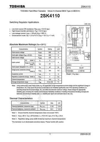
2SK4110 TOSHIBA Field Effect Transistor Silicon N Channel MOS Type ( -MOSVI) 2SK4110 Switching Regulator Applications Unit mm Low drain-source ON resistance RDS (ON) = 0.9 (typ.) High forward transfer admittance Yfs = 5.0 S (typ.) Low leakage current IDSS = 100 A (VDS = 600 V) Enhancement mode Vth = 2.0 to 4.0 V (VDS = 10 V, ID = 1 mA) Absolute Ma
2sk4113.pdf
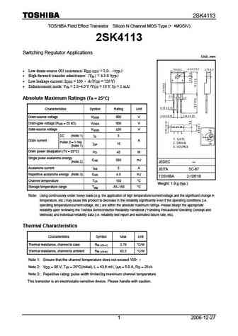
2SK4113 TOSHIBA Field Effect Transistor Silicon N Channel MOS Type ( -MOSIV) 2SK4113 Switching Regulator Applications Unit mm Low drain-source ON resistance RDS (ON) = 2.0 (typ.) High forward transfer admittance Yfs = 4.5 S (typ.) Low leakage current IDSS = 100 A (VDS = 720 V) Enhancement mode Vth = 2.0 4.0 V (VDS = 10 V, ID = 1 mA) Absolute Maximum
2sk4112.pdf
2SK4112 TOSHIBA Field Effect Transistor Silicon N Channel MOS Type ( -MOSVI) 2SK4112 Switching Regulator Applications Unit mm Low drain-source ON resistance RDS (ON) = 0.75 (typ.) High forward transfer admittance Yfs = 5.5S (typ.) Low leakage current IDSS = 100 A (VDS = 600 V) Enhancement mode Vth = 2.0 4.0 V (VDS = 10 V, ID = 1 mA) Absolute Maximum
2sc4117gr 2sc4117bl.pdf
2SC4117 TOSHIBA Transistor Silicon NPN Epitaxial Type (PCT process) 2SC4117 Audio Frequency General Purpose Amplifier Applications Unit mm AEC-Q101 Qualified (Note1) High voltage V = 120 V CEO Excellent h linearity h (I = 0.1 mA)/h (I = 2 mA) = 0.95 (typ.) FE FE C FE C High h h = 200 to 700 FE FE Low noise NF = 1dB (typ.), 10dB (max) Complemen
ssm6k411tu.pdf
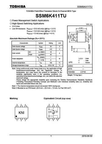
SSM6K411TU TOSHIBA Field-Effect Transistor Silicon N-Channel MOS Type SSM6K411TU Power Management Switch Applications High-Speed Switching Applications Unit mm 2.5-V drive 2.1 0.1 Low ON-resistance RDS(ON) = 23.8 m (max) (@VGS = 2.5 V) 1.7 0.1 RDS(ON) = 14.3 m (max) (@VGS = 3.5 V) RDS(ON) = 12 m (max) (@VGS = 4.5 V) 1 6 2 5 Absolute Maximum
2sk4114.pdf
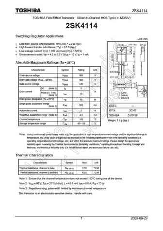
2SK4114 TOSHIBA Field Effect Transistor Silicon N-Channel MOS Type ( -MOSIV) 2SK4114 Switching Regulator Applications Unit mm Low drain-source ON resistance RDS (ON) = 2.2 (typ.) High forward transfer admittance Yfs = 3.5 S (typ.) Low leakage current IDSS = 100 A (max) (VDS = 720 V) Enhancement model Vth = 4.0 to 5.0 V (VDS = 10 V, ID = 1 mA) Abso
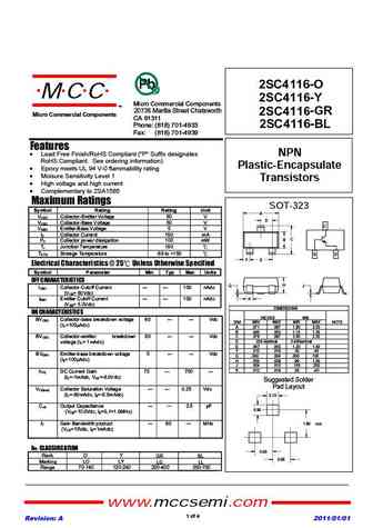
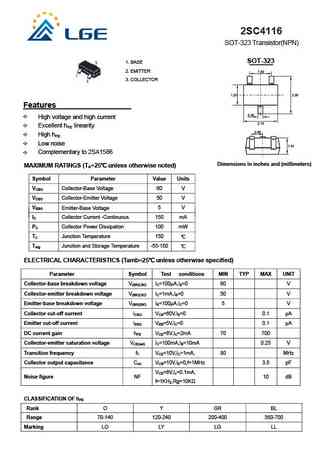
2sc4116.pdf
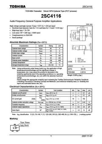
2SC4116 TOSHIBA Transistor Silicon NPN Epitaxial Type (PCT process) 2SC4116 Audio Frequency General Purpose Amplifier Applications Unit mm High voltage and high current VCEO = 50 V, IC = 150 mA (max) Excellent hFE linearity hFE (IC = 0.1 mA)/hFE (IC = 2 mA) = 0.95 (typ.) High hFE hFE = 70 700 Low noise NF = 1dB (typ.), 10dB (max) Complementary to 2SA1586
2sc4116-o 2sc4116-y 2sc4116-gr 2sc4116-bl.pdf
2SC4116 TOSHIBA Transistor Silicon NPN Epitaxial Type (PCT process) 2SC4116 Audio Frequency General Purpose Amplifier Applications Unit mm AEC-Q101 Qualified (Note1) High voltage and high current VCEO = 50 V, IC = 150 mA (max) Excellent h linearity h (I = 0.1 mA)/h (I = 2 mA) = 0.95 (typ.) FE FE C FE C High h h = 70 to 700 FE FE Low noise NF = 1dB
cph6411.pdf
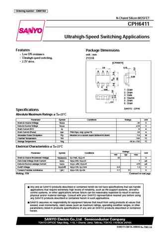
Ordering number ENN7383 CPH6411 N-Channl Silicon MOSFET CPH6411 Ultrahigh-Speed Switching Applications Features Package Dimensions Low ON-resistance. unit mm Ultrahigh-speed switching. 2151A 2.5V drive. [CPH6411] 0.15 2.9 5 6 4 0.05 1 2 3 0.95 1 Drain 2 Drain 3 Gate 4 Source 5 Drain 0.4 6 Drain SANYO CPH6 Specifications Absolute Maximum
emh2411r.pdf
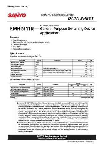
EMH2411R Ordering number ENA1421 SANYO Semiconductors DATA SHEET N-Channel Silicon MOSFET General-Purpose Switching Device EMH2411R Applications Features Low ON-resistance. Best suited for LiB charging and discharging switch. Common-drain type. 2.5V drive. Halogen free compliance. Specifications at Ta=25 C Absolute Maximum Ratings Parameter Symbol Condit
2sk4118ls.pdf

Ordering number ENA0829 2SK4118LS SANYO Semiconductors DATA SHEET N-Channel Silicon MOSFET General-Purpose Switching Device 2SK4118LS Applications Features Low ON-resistance, low input capacitance, ultrahigh-speed switching. Adoption of high reliability HVP process. Attachment workability is good by Mica-less package. Avalanche resistance guarantee. Specifications
2sk3411.pdf
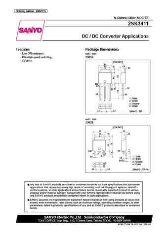
Ordering number ENN7175 2SK3411 N-Channel Silicon MOSFET 2SK3411 DC / DC Converter Applications Features Package Dimensions Low ON-resistance. unit mm Ultrahigh-speed switching. 2083B 4V drive. [2SK3411] 6.5 2.3 5.0 0.5 4 0.85 0.7 1.2 0.6 0.5 1 Gate 1 2 3 2 Drain 3 Source 4 Drain 2.3 2.3 SANYO TP unit mm 2092B [2SK3411] 6.5 2.3 5.0 0.5
2sk4119ls.pdf
Ordering number ENA0830 2SK4119LS SANYO Semiconductors DATA SHEET N-Channel Silicon MOSFET General-Purpose Switching Device 2SK4119LS Applications Features Low ON-resistance, low input capacitance, ultrahigh-speed switching. Adoption of high reliability HVP process. Attachment workability is good by Mica-less package. Avalanche resistance guarantee. Specifications
2sk4116ls.pdf

Ordering number ENA0790A 2SK4116LS SANYO Semiconductors DATA SHEET N-Channel Silicon MOSFET General-Purpose Switching Device 2SK4116LS Applications Features Low ON-resistance, low input capacitance, ultrahigh-speed switching. Adoption of high reliability HVP process. Attachment workability is good by Mica-less package. Avalanche resistance guarantee. Specifications
2sk4117ls.pdf
Ordering number ENA0791A 2SK4117LS SANYO Semiconductors DATA SHEET N-Channel Silicon MOSFET General-Purpose Switching Device 2SK4117LS Applications Features Low ON-resistance, low input capacitance, ultrahigh-speed switching. Adoption of high reliability HVP process. Attachment workability is good by Mica-less package. Avalanche resistance guarantee. Specifications
ech8411.pdf
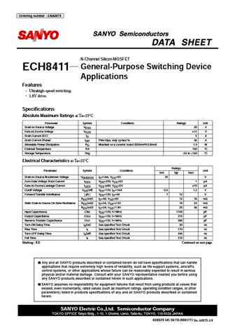
Ordering number ENA0073 ECH8411 N-Channel Silicon MOSFET General-Purpose Switching Device ECH8411 Applications Features Ultrahigh-speed switching. 1.8V drive. Specifications Absolute Maximum Ratings at Ta=25 C Parameter Symbol Conditions Ratings Unit Drain-to-Source Voltage VDSS 20 V Gate-to-Source Voltage VGSS 12 V Drain Current (DC) ID 9 A Drain Current (Pulse) IDP
2sc4119.pdf
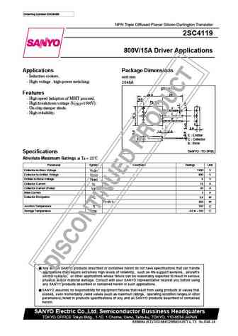
Ordering number EN2548B NPN Triple Diffused Planar Silicon Darlington Transistor 2SC4119 800V/15A Driver Applications Applications Package Dimensions Induction cookers. unit mm High-voltage , high-power switching. 2048A [2SC4119] Features High speed (adoption of MBIT process). High breakdown voltage (VCBO=1500V). On-chip damper diode. High reliability. E
2sc4110.pdf
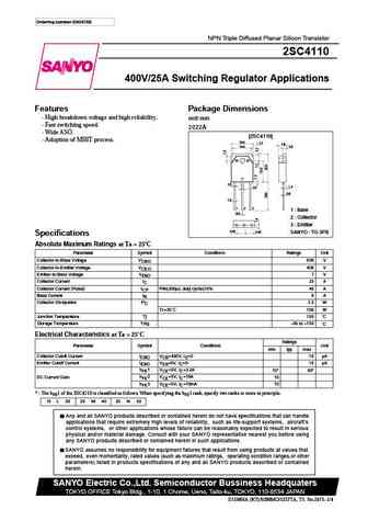
Ordering number EN2475B NPN Triple Diffused Planar Silicon Transistor 2SC4110 400V/25A Switching Regulator Applications Features Package Dimensions High breakdown voltage and high reliability. unit mm Fast switching speed. 2022A Wide ASO. [2SC4110] Adoption of MBIT process. 15.6 3.2 4.8 14.0 2.0 1.6 1.4 2.0 0.6 1.0 1 2 3 1 Base 0.6 2 Collector 3 E
pn4117 pn4118 pn4119 mmbf4117 mmbf4118 mmbf4119.pdf
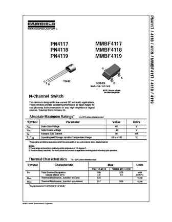
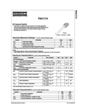
PN4117 MMBF4117 PN4118 MMBF4118 PN4119 MMBF4119 G S G TO-92 S SOT-23 D D Mark 61A / 61C / 61E NOTE Source & Drain are interchangeable N-Channel Switch This device is designed for low current DC and audio applications. These devices provide excellent performance as input stages for sub-picoamp instrumentation or any high impedance signal sources. Sourced from Process 53. Abso
pn4117a.pdf
PN4117A N-Channel Switch This device is designed for low current DC and audio application. These devices provide excellent performance as input stages for sub- picoamp instrumentation or any high impedance signal sources. Sourced from process 53. TO-92 1 1. Drain 2. Source 3. Gate Absolute Maximum Ratings * TA=25 C unless otherwise noted Symbol Parameter Value Units VDG Dra
fjv4112r.pdf

FJV4112R Switching Application (Bias Resistor Built In) Switching circuit, Inverter, Interface circuit, Driver Circuit 3 Built in bias Resistor (R=47K ) Complement to FJV3112R 2 SOT-23 1 1. Base 2. Emitter 3. Collector Equivalent Circuit C Marking R R82 B PNP Epitaxial Silicon Transistor E Absolute Maximum Ratings Ta=25 C unless otherwise noted Symbol Paramete
fjv4111r.pdf

FJV4111R Switching Application (Bias Resistor Built In) Switching circuit, Inverter, Interface circuit, Driver Circuit 3 Built in bias Resistor (R=22K ) Complement to FJV3111R 2 SOT-23 1 1. Base 2. Emitter 3. Collector Equivalent Circuit C Marking R R81 B PNP Epitaxial Silicon Transistor E Absolute Maximum Ratings Ta=25 C unless otherwise noted Symbol Paramete
fjv4113r.pdf
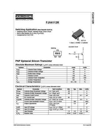
FJV4113R Switching Application (Bias Resistor Built In) Switching circuit, Inverter, Interface circuit, Driver Circuit 3 Built in bias Resistor (R1=2.2K , R2=47K ) Complement to FJV3113R 2 SOT-23 1 1. Base 2. Emitter 3. Collector Equivalent Circuit C Marking R1 B R83 R2 PNP Epitaxial Silicon Transistor E Absolute Maximum Ratings Ta=25 C unless otherwise note
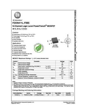
fdd9411 f085.pdf
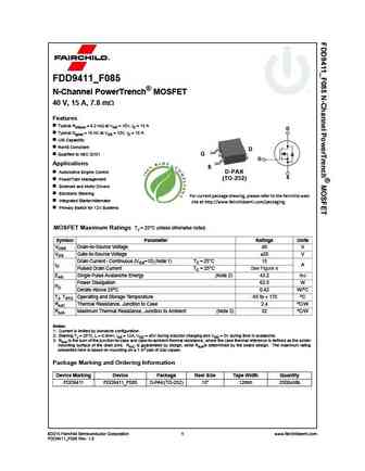
April 2015 FDD9411_F085 N-Channel PowerTrench MOSFET 40 V, 15 A, 7.8 m Features Typical RDS(on) = 6.2 m at VGS = 10V, ID = 15 A D Typical Qg(tot) = 15 nC at VGS = 10V, ID = 15 A UIS Capability RoHS Compliant D Qualified to AEC Q101 G G Applications S Automotive Engine Control D-PAK TO-252 S (TO-252) PowerTrain Management Solenoid and Motor Drivers Elec
fjv4110r.pdf
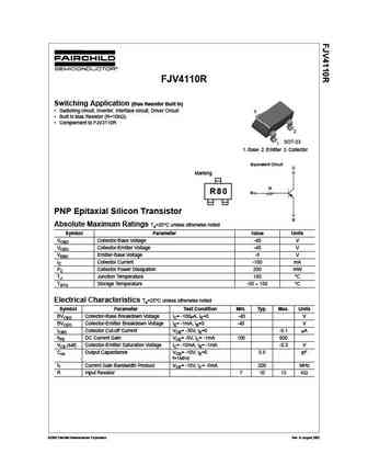
FJV4110R Switching Application (Bias Resistor Built In) Switching circuit, Inverter, Interface circuit, Driver Circuit 3 Built in bias Resistor (R=10K ) Complement to FJV3110R 2 SOT-23 1 1. Base 2. Emitter 3. Collector Equivalent Circuit C Marking R R80 B PNP Epitaxial Silicon Transistor E Absolute Maximum Ratings Ta=25 C unless otherwise noted Symbol Paramete
fjv4114r.pdf

FJV4114R Switching Application (Bias Resistor Built In) Switching circuit, Inverter, Interface circuit, Driver Circuit 3 Built in bias Resistor (R1 =4.7K , R2=47K ) Complement to FJV3114R 2 SOT-23 1 1. Base 2. Emitter 3. Collector Equivalent Circuit C Marking R1 B R84 R2 PNP Epitaxial Silicon Transistor E Absolute Maximum Ratings Ta=25 C unless otherwise not
2sk2411-z.pdf
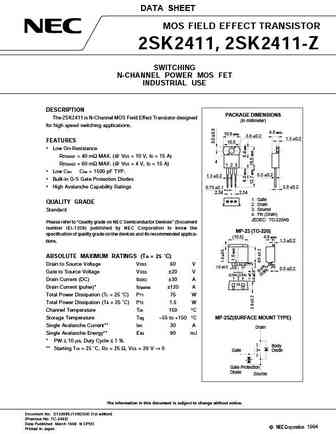
DATA SHEET MOS FIELD EFFECT TRANSISTOR 2SK2411, 2SK2411-Z SWITCHING N-CHANNEL POWER MOS FET INDUSTRIAL USE DESCRIPTION PACKAGE DIMENSIONS The 2SK2411 is N-Channel MOS Field Effect Transistor designed (in millimeter) for high speed switching applications. 4.8 MAX. 10.6 MAX. 3.6 0.2 1.3 0.2 FEATURES 10.0 Low On-Resistance RDS(on)1 = 40 m MAX. (@ VGS = 10 V, ID = 15 A)
2sj411.pdf
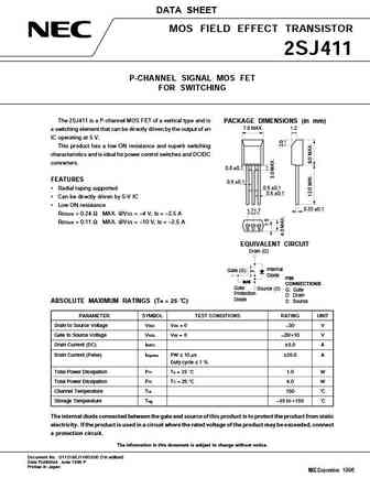
DATA SHEET MOS FIELD EFFECT TRANSISTOR 2SJ411 P-CHANNEL SIGNAL MOS FET FOR SWITCHING The 2SJ411 is a P-channel MOS FET of a vertical type and is PACKAGE DIMENSIONS (in mm) 7.0 MAX. 1.2 a switching element that can be directly driven by the output of an IC operating at 5 V. This product has a low ON resistance and superb switching characteristics and is ideal for power control switche
pbss4112pan.pdf
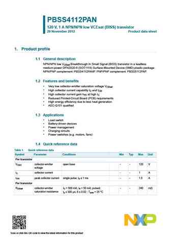
PBSS4112PAN 120 V, 1 A NPN/NPN low VCEsat (BISS) transistor 29 November 2012 Product data sheet 1. Product profile 1.1 General description NPN/NPN low VCEsat Breakthrough In Small Signal (BISS) transistor in a leadless medium power DFN2020-6 (SOT1118) Surface-Mounted Device (SMD) plastic package. NPN/PNP complement PBSS4112PANP. PNP/PNP complement PBSS5112PAP. 1.2 Features and benefit
pbss4112panp.pdf
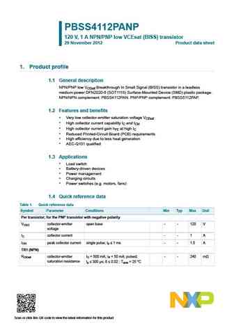
PBSS4112PANP 120 V, 1 A NPN/PNP low VCEsat (BISS) transistor 29 November 2012 Product data sheet 1. Product profile 1.1 General description NPN/PNP low VCEsat Breakthrough In Small Signal (BISS) transistor in a leadless medium power DFN2020-6 (SOT1118) Surface-Mounted Device (SMD) plastic package. NPN/NPN complement PBSS4112PAN. PNP/PNP complement PBSS5112PAP. 1.2 Features and benefit
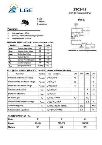
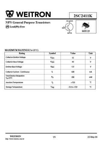
2sc2411k.pdf
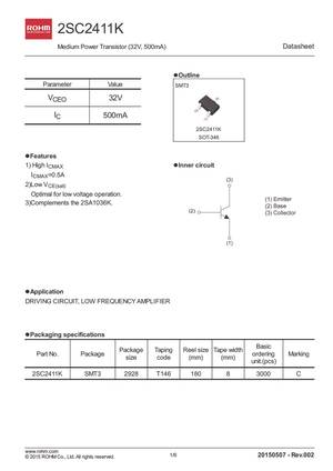
2SC2411K Datasheet Medium Power Transistor (32V, 500mA) lOutline l Parameter Value SMT3 VCEO 32V IC 500mA 2SC2411K SOT-346 lFeatures l 1) High ICMAX lInner circuit l ICMAX=0.5A 2)Low VCE(sat) Optimal for low voltage operation. 3)Complements the 2SA1036K. lApplication l DRIVING CIRCUIT, LOW FREQ
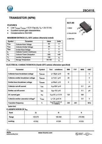
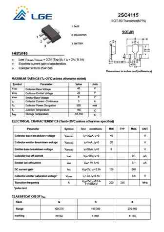
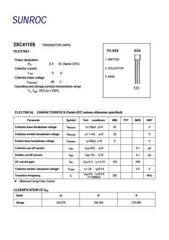
2sc4115s.pdf
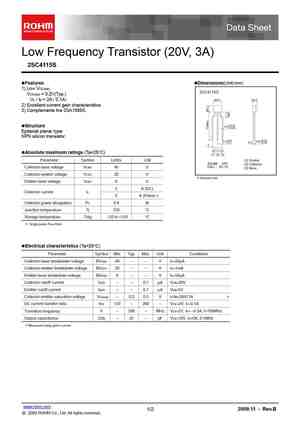
Low Frequency Transistor (20V, 3A) 2SC4115S Features Dimensions(Unit mm) 1) Low VCE(sat). 2SC4115S VCE(sat) = 0.2V(Typ.) IC / IB = 2A / 0.1A 4 0.2 2 0.2 2) Excellent current gain characteristics. 3) Complements the 2SA1585S. Structure 0.45+0.15 -0.05 Epitaxial planar type NPN silicon transistor 0.45+0.15 2.5+0.4 0.5 -0.05 -0.1 5 Absolute maximum ratings (Ta
2sc2411kfra.pdf
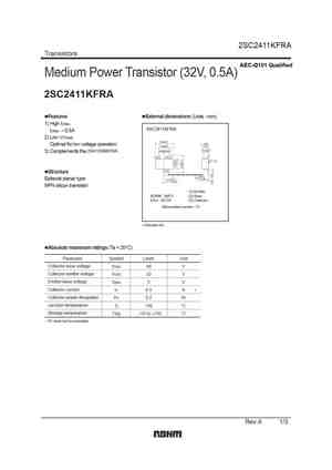
2SC2411KFRA 2SC2411K Transistors AEC-Q101 Qualified Medium Power Transistor (32V, 0.5A) 2SC2411K 2SC2411KFRA Features External dimensions (Units mm) 1) High ICMax. 2SC2411KFRA 2SC2411K ICMax. = 0.5A 2) Low VCE(sat). 2.9 0.2 Optimal for low voltage operation. 1.1+0.2 1.9 0.2 -0.1 0.8 0.1 0.95 0.95 2SA1036KFRA 3) Complements the 2SA1036K. (1) (2) 0 0.1 (3)
2n4117a pn4117a sst4117 2n4118a pn4118a sst4118 2n4119a pn4119a sst4119.pdf
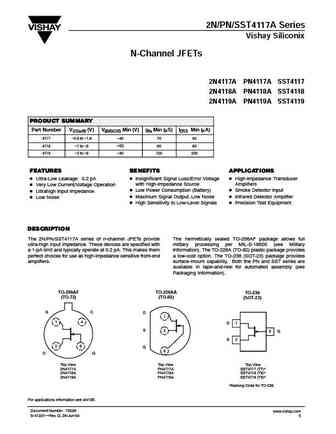
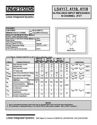
2N/PN/SST4117A Series Vishay Siliconix N-Channel JFETs 2N4117A PN4117A SST4117 2N4118A PN4118A SST4118 2N4119A PN4119A SST4119 PRODUCT SUMMARY Part Number VGS(off) (V) V(BR)GSS Min (V) gfs Min (mS) IDSS Min (mA) 4117 -0.6 to -1.8 -40 70 30 4118 -1 to -3 -40 80 80 4119 -2 to -6 -40 100 200 FEATURES BENEFITS APPLICATIONS D Ultra-Low Leakage 0.2 pA D Insignificant Signal Loss/Error Vo
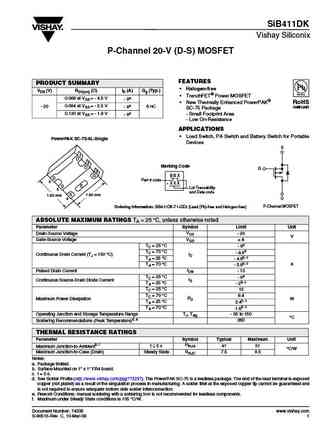
si4110dy.pdf
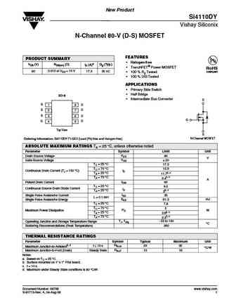
New Product Si4110DY Vishay Siliconix N-Channel 80-V (D-S) MOSFET FEATURES PRODUCT SUMMARY Halogen-free VDS (V) RDS(on) ( ) ID (A)a Qg (Typ.) TrenchFET Power MOSFET RoHS 0.013 at VGS = 10 V 80 17.3 35 nC COMPLIANT 100 % Rg Tested 100 % UIS Tested APPLICATIONS Primary Side Switch Half Bridge SO-8 Intermediate Bus Converter D S 1
si4411dy.pdf
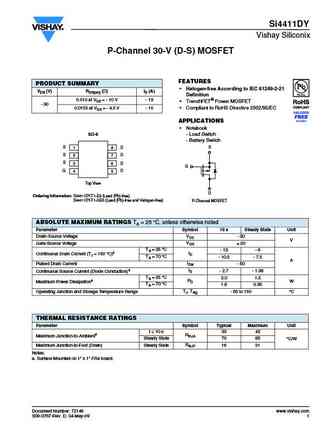
Si4411DY Vishay Siliconix P-Channel 30-V (D-S) MOSFET FEATURES PRODUCT SUMMARY Halogen-free According to IEC 61249-2-21 VDS (V) RDS(on) ( )ID (A) Definition 0.010 at VGS = - 10 V - 13 TrenchFET Power MOSFET - 30 0.0155 at VGS = - 4.5 V - 10 Compliant to RoHS Directive 2002/95/EC APPLICATIONS Notebook SO-8 - Load Switch - Battery Switch S S 1 8 D S D
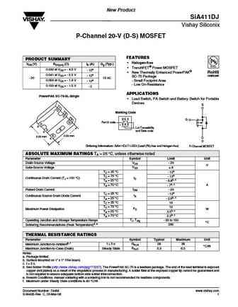
si7411dn.pdf
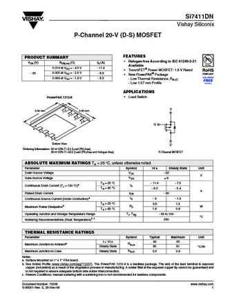
Si7411DN Vishay Siliconix P-Channel 20-V (D-S) MOSFET FEATURES PRODUCT SUMMARY Halogen-free According to IEC 61249-2-21 VDS (V) RDS(on) ( )ID (A) Available 0.019 at VGS = - 4.5 V - 11.4 TrenchFET Power MOSFET 1.8 V Rated 0.025 at VGS = - 2.5 V - 20 - 9.9 New PowerPAK Package 0.034 at VGS = - 1.8 V - 8.5 - Low Thermal Resistance, RthJC - Low 1.07 mm Pro
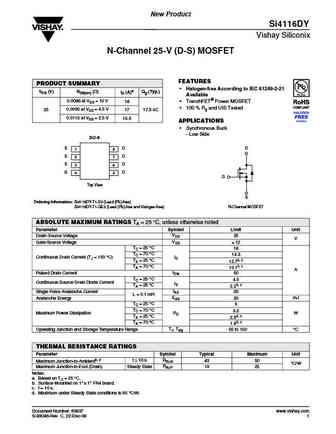
si4114dy.pdf
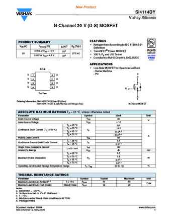
New Product Si4114DY Vishay Siliconix N-Channel 20-V (D-S) MOSFET FEATURES PRODUCT SUMMARY Halogen-free According to IEC 61249-2-21 VDS (V) RDS(on) ( ) ID (A)a Qg (Typ.) Definition 0.006 at VGS = 10 V TrenchFET Power MOSFET 20e 20 27.5 nC 100 % Rg and UIS Tested 0.007 at VGS = 4.5 V 20e Compliant to RoHS Directive 2002/95/EC APPLICATIONS Low-Si
si1411dh.pdf
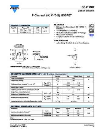
Si1411DH Vishay Siliconix P-Channel 150 V (D-S) MOSFET FEATURES PRODUCT SUMMARY Halogen-free According to IEC 61249-2-21 VDS (V) RDS(on) ( )ID (A) Qg (Typ.) Definition 2.6 at VGS = - 10 V - 0.52 TrenchFET Power MOSFETS - 150 4.2 nC 2.7 at VGS = - 6 V - 0.51 Small, Thermally Enhanced SC-70 Package Ultra Low On-Resistance Compliant to RoHS Directive 200
sia411dj.pdf
New Product SiA411DJ Vishay Siliconix P-Channel 20-V (D-S) MOSFET FEATURES PRODUCT SUMMARY Halogen-free VDS (V) RDS(on) ( )ID (A) Qg (Typ.) TrenchFET Power MOSFET 0.030 at VGS = - 4.5 V - 12a New Thermally Enhanced PowerPAK RoHS 0.041 at VGS = - 2.5 V - 12a COMPLIANT SC-70 Package - 20 15 nC 0.056 at VGS = - 1.8 V - Small Footprint Area - 12a - Low On-
si4116dy.pdf
New Product Si4116DY Vishay Siliconix N-Channel 25-V (D-S) MOSFET FEATURES PRODUCT SUMMARY Halogen-free According to IEC 61249-2-21 VDS (V) RDS(on) ( ) ID (A)a Qg (Typ.) Available 0.0086 at VGS = 10 V 18 TrenchFET Power MOSFET 100 % Rg and UIS Tested 0.0095 at VGS = 4.5 V 25 17 17.5 nC 0.0115 at VGS = 2.5 V 15.5 APPLICATIONS Synchronous Buck - Low S
si5411edu.pdf
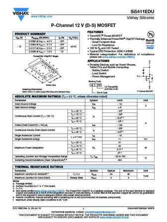
Si5411EDU www.vishay.com Vishay Siliconix P-Channel 12 V (D-S) MOSFET FEATURES PRODUCT SUMMARY TrenchFET Power MOSFET VDS (V) RDS(on) ( ) (Max.) ID (A) Qg (Typ.) Thermally Enhanced PowerPAK ChipFET Package 0.0082 at VGS = - 4.5 V - 25a - Small Footprint Area 0.0094 at VGS = - 3.7 V - 25a - Low On-Resistance - 12 43 nC 0.0117 at VGS = - 2.5 V - 25a 100 % Rg and UI
sib411dk.pdf
SiB411DK Vishay Siliconix P-Channel 20-V (D-S) MOSFET FEATURES PRODUCT SUMMARY Halogen-free VDS (V) RDS(on) ( )ID (A) Qg (Typ.) TrenchFET Power MOSFET 0.066 at VGS = - 4.5 V - 9a New Thermally Enhanced PowerPAK RoHS 0.094 at VGS = - 2.5 V - 20 - 9a 6 nC COMPLIANT SC-75 Package 0.130 at VGS = - 1.8 V - Small Footprint Area - 9a - Low On-Resistance APPLI
2n2411 2n2412.pdf
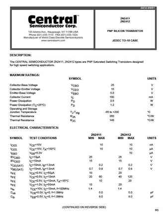
DATA SHEET 2N2411 2N2412 PNP SILICON TRANSISTOR JEDEC TO-18 CASE DESCRIPTION The CENTRAL SEMICONDUCTOR 2N2411, 2N2412 types are PNP Saturated Switching Transistors designed for high speed switching applications. MAXIMUM RATINGS SYMBOL UNITS Collector-Base Voltage VCBO 25 V Collector-Emitter Voltage VCEO 15 V Emitter-Base Voltage VEBO 5.0 V Collector Current IC 100 mA
auirfs4115-7p.pdf
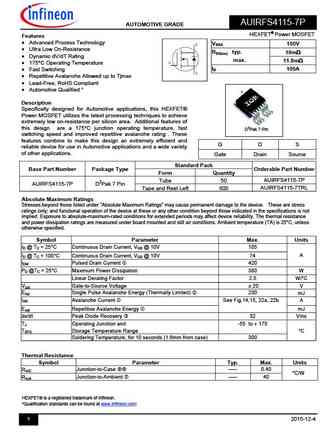
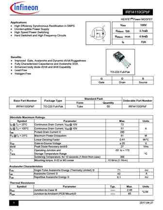
AUIRFS4115-7P AUTOMOTIVE GRADE HEXFET Power MOSFET Features Advanced Process Technology VDSS 150V Ultra Low On-Resistance RDS(on) typ. 10m Dynamic dV/dT Rating max. 11.8m 175 C Operating Temperature ID 105A Fast Switching Repetitive Avalanche Allowed up to Tjmax Lead-Free, RoHS Compliant Automotive Qualified * Descrip
irfi4110gpbf.pdf
IRFI4110GPbF HEXFET Power MOSFET Applications VDSS 100V High Efficiency Synchronous Rectification in SMPS Uninterruptible Power Supply RDS(on) typ. 3.7m High Speed Power Switching Hard Switched and High Frequency Circuits RDS(on) max. 4.5m ID 72A Benefits Improved Gate, Avalanche and Dynamic dV/dt Ruggedness Fully Characterized Capac
auirfs4115 auirfsl4115.pdf
AUIRFS4115 AUTOMOTIVE GRADE AUIRFSL4115 HEXFET Power MOSFET VDSS 150V Features Advanced Process Technology RDS(on) typ. 10.3m Ultra Low On-Resistance max. 12.1m 175 C Operating Temperature Fast Switching ID 99A Repetitive Avalanche Allowed up to Tjmax Lead-Free, RoHS Compliant D D Automotive Qualified * Description S S
auirfp4110.pdf
AUTOMOTIVE GRADE AUIRFP4110 HEXFET Power MOSFET Features Advanced Process Technology VDSS 100V D Ultra Low On-Resistance RDS(on) typ. 3.7m Enhanced dV/dT and dI/dT capability 4.5m max 175 C Operating Temperature G ID (Silicon Limited) 180A Fast Switching S Repetitive Avalanche Allowed up to Tjmax ID (Package Lim
2sc2411-r.pdf

MCC 2SC2411-P Micro Commercial Components TM 20736 Marilla Street Chatsworth Micro Commercial Components 2SC2411-Q CA 91311 Phone (818) 701-4933 2SC2411-R Fax (818) 701-4939 Features Lead Free Finish/RoHS Compliant ("P" Suffix designates RoHS Compliant. See ordering information) NPN Silicon High IC. ICMax.= 0.5 A Low VCE(sat).Optimal for low voltage operation.
2sc4116-y.pdf
2SC4116-O MCC 2SC4116-Y Micro Commercial Components TM 20736 Marilla Street Chatsworth 2SC4116-GR Micro Commercial Components CA 91311 Phone (818) 701-4933 2SC4116-BL Fax (818) 701-4939 Features Lead Free Finish/RoHS Compliant ("P" Suffix designates NPN RoHS Compliant. See ordering information) Plastic-Encapsulate Epoxy meets UL 94 V-0 flammability rating Moisur
2sc2411-p.pdf

MCC 2SC2411-P Micro Commercial Components TM 20736 Marilla Street Chatsworth Micro Commercial Components 2SC2411-Q CA 91311 Phone (818) 701-4933 2SC2411-R Fax (818) 701-4939 Features Lead Free Finish/RoHS Compliant ("P" Suffix designates RoHS Compliant. See ordering information) NPN Silicon High IC. ICMax.= 0.5 A Low VCE(sat).Optimal for low voltage operation.
2sc4116-bl.pdf

2SC4116-O MCC 2SC4116-Y Micro Commercial Components TM 20736 Marilla Street Chatsworth 2SC4116-GR Micro Commercial Components CA 91311 Phone (818) 701-4933 2SC4116-BL Fax (818) 701-4939 Features Lead Free Finish/RoHS Compliant ("P" Suffix designates NPN RoHS Compliant. See ordering information) Plastic-Encapsulate Epoxy meets UL 94 V-0 flammability rating Moisur
2sc2411-q.pdf
MCC 2SC2411-P Micro Commercial Components TM 20736 Marilla Street Chatsworth Micro Commercial Components 2SC2411-Q CA 91311 Phone (818) 701-4933 2SC2411-R Fax (818) 701-4939 Features Lead Free Finish/RoHS Compliant ("P" Suffix designates RoHS Compliant. See ordering information) NPN Silicon High IC. ICMax.= 0.5 A Low VCE(sat).Optimal for low voltage operation.
2sc4116-o.pdf

2SC4116-O MCC 2SC4116-Y Micro Commercial Components TM 20736 Marilla Street Chatsworth 2SC4116-GR Micro Commercial Components CA 91311 Phone (818) 701-4933 2SC4116-BL Fax (818) 701-4939 Features Lead Free Finish/RoHS Compliant ("P" Suffix designates NPN RoHS Compliant. See ordering information) Plastic-Encapsulate Epoxy meets UL 94 V-0 flammability rating Moisur
2sc4115s-q.pdf
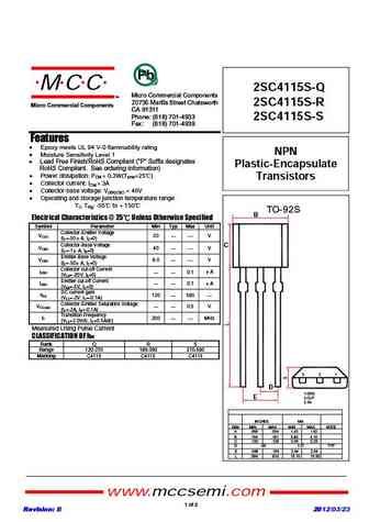
MCC 2SC4115S-Q Micro Commercial Components TM 20736 Marilla Street Chatsworth 2SC4115S-R Micro Commercial Components CA 91311 Phone (818) 701-4933 2SC4115S-S Fax (818) 701-4939 Features Epoxy meets UL 94 V-0 flammability rating NPN Moisture Sensitivity Level 1 Lead Free Finish/RoHS Compliant ("P" Suffix designates Plastic-Encapsulate RoHS Compliant. See orderin
2sc4116-gr.pdf

2SC4116-O MCC 2SC4116-Y Micro Commercial Components TM 20736 Marilla Street Chatsworth 2SC4116-GR Micro Commercial Components CA 91311 Phone (818) 701-4933 2SC4116-BL Fax (818) 701-4939 Features Lead Free Finish/RoHS Compliant ("P" Suffix designates NPN RoHS Compliant. See ordering information) Plastic-Encapsulate Epoxy meets UL 94 V-0 flammability rating Moisur
fdd9411l-f085.pdf
FDD9411L-F085 N-Channel Logic Level PowerTrench MOSFET 40 V, 25 A, 7.0 m Features Typical RDS(on) = 5.6 m at VGS = 10V, ID = 20 A D Typical Qg(tot) = 18 nC at VGS = 10V, ID = 20 A UIS Capability RoHS Compliant D Qualified to AEC Q101 G G Applications S Automotive Engine Control D-PAK TO-252 S (TO-252) PowerTrain Management Solenoid and Motor Drivers Electr
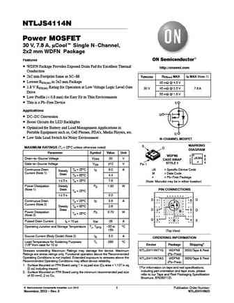
ntljs4114n.pdf
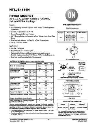
NTLJS4114N Power MOSFET 30 V, 7.8 A, mCoolt Single N-Channel, 2x2 mm WDFN Package Features WDFN Package Provides Exposed Drain Pad for Excellent Thermal http //onsemi.com Conduction 2x2 mm Footprint Same as SC-88 V(BR)DSS RDS(on) MAX ID MAX (Note 1) Lowest RDS(on) in 2x2 mm Package 35 mW @ 4.5 V 1.8 V RDS(on) Rating for Operation at Low Voltage Logic Level Gate 30 V
nths4111pt1g.pdf
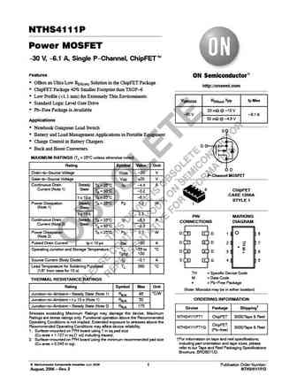
NTHS4111P Power MOSFET -30 V, -6.1 A, Single P-Channel, ChipFETt Features Offers an Ultra Low RDS(on) Solution in the ChipFET Package http //onsemi.com ChipFET Package 40% Smaller Footprint than TSOP-6 Low Profile (
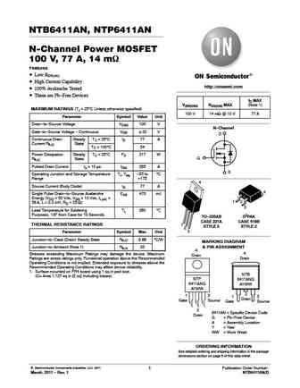
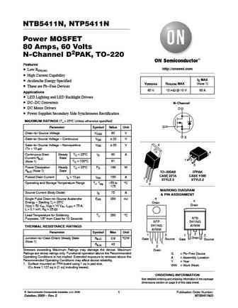
ntb6411n ntp6411n.pdf

NTB6411AN, NTP6411AN N-Channel Power MOSFET 100 V, 77 A, 14 mW Features Low RDS(on) High Current Capability http //onsemi.com 100% Avalanche Tested These are Pb-Free Devices ID MAX V(BR)DSS RDS(ON) MAX (Note 1) MAXIMUM RATINGS (TJ = 25 C Unless otherwise specified) 100 V 14 mW @ 10 V 77 A Parameter Symbol Value Unit Drain-to-Source Voltage VDSS 100 V N-Channel G
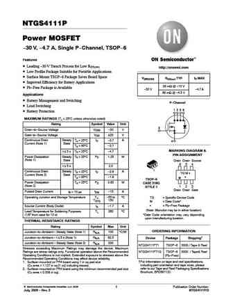
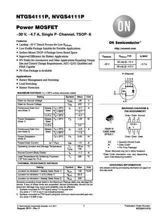
ntgs4111p nvgs4111p.pdf
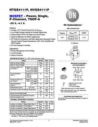
NTGS4111P, NVGS4111P MOSFET Power, Single, P-Channel, TSOP-6 -30 V, -4.7 A Features http //onsemi.com Leading -30 V Trench Process for Low RDS(on) Low Profile Package Suitable for Portable Applications V(BR)DSS RDS(on) TYP ID MAX Surface Mount TSOP-6 Package Saves Board Space 38 mW @ -10 V Improved Efficiency for Battery Applications -30 V -4.7 A 68 mW @ -4.5 V
fdd9411-f085.pdf
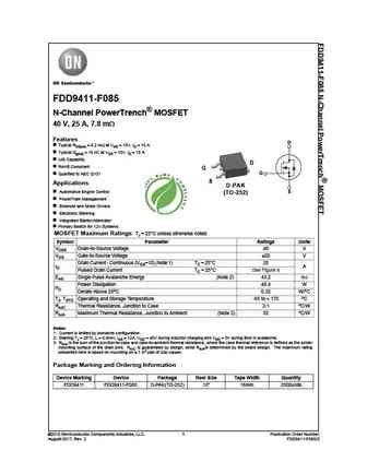
FDD9411-F085 N-Channel PowerTrench MOSFET 40 V, 25 A, 7.8 m Features D Typical RDS(on) = 6.2 m at VGS = 10V, ID = 15 A Typical Qg(tot) = 15 nC at VGS = 10V, ID = 15 A UIS Capability D RoHS Compliant G G Qualified to AEC Q101 S Applications D-PAK TO-252 Automotive Engine Control S (TO-252) PowerTrain Management Solenoid and Motor Drivers Electronic Steerin
ntb6411ang nvb6411an.pdf
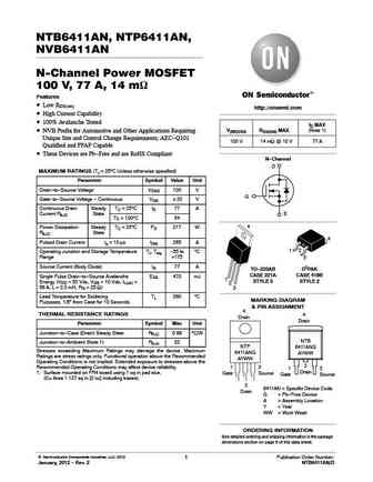
NTB6411AN, NTP6411AN, NVB6411AN N-Channel Power MOSFET 100 V, 77 A, 14 mW Features Low RDS(on) http //onsemi.com High Current Capability 100% Avalanche Tested ID MAX NVB Prefix for Automotive and Other Applications Requiring V(BR)DSS RDS(ON) MAX (Note 1) Unique Site and Control Change Requirements; AEC-Q101 100 V 14 mW @ 10 V 77 A Qualified and PPAP Capable The
ntljd4116n-d.pdf
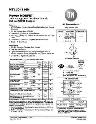
NTLJD4116N Power MOSFET 30 V, 4.6 A, mCoolt Dual N-Channel, 2x2 mm WDFN Package Features WDFN Package Provides Exposed Drain Pad for Excellent Thermal http //onsemi.com Conduction 2x2 mm Footprint Same as SC-88 V(BR)DSS RDS(on) MAX ID MAX (Note 1) Lowest RDS(on) Solution in 2x2 mm Package 70 mW @ 4.5 V 1.5 V RDS(on) Rating for Operation at Low Voltage Gate Drive Logi
ntgs4111p.pdf
NTGS4111P Power MOSFET -30 V, -4.7 A, Single P-Channel, TSOP-6 Features Leading -30 V Trench Process for Low RDS(on) http //onsemi.com Low Profile Package Suitable for Portable Applications Surface Mount TSOP-6 Package Saves Board Space V(BR)DSS RDS(on) TYP ID MAX Improved Efficiency for Battery Applications 38 mW @ -10 V Pb-Free Package is Available -30 V -4.7 A
ntljs4114nt1g.pdf
NTLJS4114N Power MOSFET 30 V, 7.8 A, mCoolt Single N-Channel, 2x2 mm WDFN Package Features WDFN Package Provides Exposed Drain Pad for Excellent Thermal http //onsemi.com Conduction 2x2 mm Footprint Same as SC-88 V(BR)DSS RDS(on) MAX ID MAX (Note 1) Lowest RDS(on) in 2x2 mm Package 35 mW @ 4.5 V 1.8 V RDS(on) Rating for Operation at Low Voltage Logic Level Gate 30 V
nvgs4111p.pdf
NTGS4111P, NVGS4111P Power MOSFET -30 V, -4.7 A, Single P-Channel, TSOP-6 Features Leading -30 V Trench Process for Low RDS(on) Low Profile Package Suitable for Portable Applications http //onsemi.com Surface Mount TSOP-6 Package Saves Board Space V(BR)DSS RDS(on) TYP ID MAX Improved Efficiency for Battery Applications NV Prefix for Automotive and Other Applications
ntp6411ang.pdf
NTB6411AN, NTP6411AN N-Channel Power MOSFET 100 V, 77 A, 14 mW Features Low RDS(on) High Current Capability http //onsemi.com 100% Avalanche Tested These are Pb-Free Devices ID MAX V(BR)DSS RDS(ON) MAX (Note 1) MAXIMUM RATINGS (TJ = 25 C Unless otherwise specified) 100 V 14 mW @ 10 V 77 A Parameter Symbol Value Unit Drain-to-Source Voltage VDSS 100 V N-Channel G
ntmfs4119n.pdf
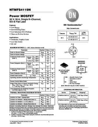
NTMFS4119N Power MOSFET 30 V, 30 A, Single N-Channel, SO-8 Flat Lead Features Low RDS(on) http //onsemi.com Fast Switching Times Low Inductance SO-8 Package ID Max V(BR)DSS RDS(on) Typ (Note 1) These are Pb-Free Devices 2.3 mW @ 10 V Applications 30 V 30 A 3.1 mW @ 4.5 V Notebooks, Graphics Cards Low Side Switch DC-DC D MAXIMUM RATINGS (TJ = 25 C

ntmfs4119nt1g.pdf
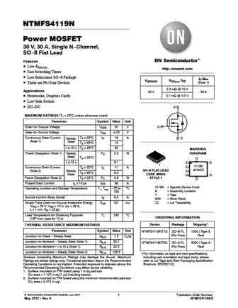
NTMFS4119N Power MOSFET 30 V, 30 A, Single N-Channel, SO-8 Flat Lead Features Low RDS(on) http //onsemi.com Fast Switching Times Low Inductance SO-8 Package ID Max V(BR)DSS RDS(on) Typ (Note 1) These are Pb-Free Devices 2.3 mW @ 10 V Applications 30 V 30 A 3.1 mW @ 4.5 V Notebooks, Graphics Cards Low Side Switch DC-DC D MAXIMUM RATINGS (TJ = 25 C
ntgs4111pt1.pdf

NTGS4111P Power MOSFET -30 V, -4.7 A, Single P-Channel, TSOP-6 Features Leading -30 V Trench Process for Low RDS(on) http //onsemi.com Low Profile Package Suitable for Portable Applications Surface Mount TSOP-6 Package Saves Board Space V(BR)DSS RDS(on) TYP ID MAX Improved Efficiency for Battery Applications 38 mW @ -10 V Pb-Free Package is Available -30 V -4.7 A
dra4114e.pdf
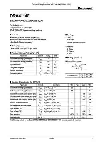
This product complies with the RoHS Directive (EU 2002/95/EC). DRA4114E Silicon PNP epitaxial planar type For digital circuits Complementary to DRC4114E DRA2114E in NS through hole type package Features Package Low collector-emitter saturation voltage VCE(sat) Code Contributes to miniaturization of sets, mount area reduction NS-B2-B-B Eco-friendly Halogen-free
un4110q un4110r un4110s un4111 un4112 un4113 un4114 un4115q un4115r un4115s un4116q un4116r un4116s un4117q un4117r un4117s.pdf
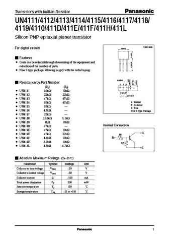
Transistors with built-in Resistor UN4111/4112/4113/4114/4115/4116/4117/4118/ 4119/4110/411D/411E/411F/411H/411L Silicon PNP epitaxial planer transistor Unit mm For digital circuits 4.0 0.2 Features Costs can be reduced through downsizing of the equipment and reduction of the number of parts. New S type package, allowing supply with the radial taping. marking Resistance by Part N
dra4113z.pdf

This product complies with the RoHS Directive (EU 2002/95/EC). DRA4113Z Silicon PNP epitaxial planar type For digital circuits Complementary to DRC4113Z DRA2113Z in NS through hole type package Features Package Low collector-emitter saturation voltage VCE(sat) Code Contributes to miniaturization of sets, mount area reduction NS-B2-B-B Eco-friendly Halogen-free
mtm68411.pdf
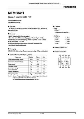
This product complies with the RoHS Directive (EU 2002/95/EC). MTM68411 Silicon P-channel MOS FET For load switch circuits For switching circuits Package Overview Code MTM68411 is the low ON resistance dual P-channel MOS FET designed for WMini8-F1 load switch circuits. Package dimension clicks here. Click! Features Pin Name Dual P-channel MOS FET in o
drc4114w.pdf
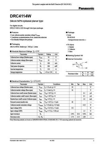
This product complies with the RoHS Directive (EU 2002/95/EC). DRC4114W Silicon NPN epitaxial planar type For digital circuits DRC2114W in NS through hole type package Features Package Low collector-emitter saturation voltage VCE(sat) Code Contributes to miniaturization of sets, mount area reduction NS-B2-B-B Eco-friendly Halogen-free package Package dimension
dra4114t.pdf

This product complies with the RoHS Directive (EU 2002/95/EC). DRA4114T Silicon PNP epitaxial planar type For digital circuits Complementary to DRC4114T DRA2114T in NS through hole type package Features Package High forward current transfer ratio hFE with excellent linearity Code Low collector-emitter saturation voltage VCE(sat) NS-B2-B-B Contributes to miniat
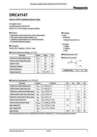
drc4114y.pdf

This product complies with the RoHS Directive (EU 2002/95/EC). DRC4114Y Silicon NPN epitaxial planar type For digital circuits Complementary to DRA4114Y DRC2114Y in NS through hole type package Features Package Low collector-emitter saturation voltage VCE(sat) Code Contributes to miniaturization of sets, mount area reduction NS-B2-B-B Eco-friendly Halogen-free
drc4113z.pdf
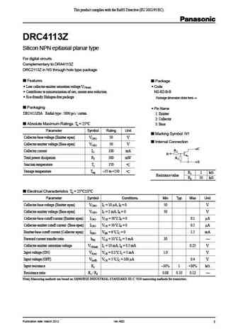
This product complies with the RoHS Directive (EU 2002/95/EC). DRC4113Z Silicon NPN epitaxial planar type For digital circuits Complementary to DRA4113Z DRC2113Z in NS through hole type package Features Package Low collector-emitter saturation voltage VCE(sat) Code Contributes to miniaturization of sets, mount area reduction NS-B2-B-B Eco-friendly Halogen-free
drc4114t.pdf
This product complies with the RoHS Directive (EU 2002/95/EC). DRC4114T Silicon NPN epitaxial planar type For digital circuits Complementary to DRA4114T DRC2114T in NS through hole type package Features Package High forward current transfer ratio hFE with excellent linearity Code Low collector-emitter saturation voltage VCE(sat) NS-B2-B-B Contributes to miniat
dra4114y.pdf
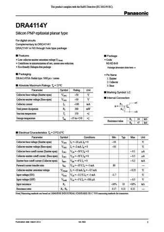
This product complies with the RoHS Directive (EU 2002/95/EC). DRA4114Y Silicon PNP epitaxial planar type For digital circuits Complementary to DRC4114Y DRA2114Y in NS through hole type package Features Package Low collector-emitter saturation voltage VCE(sat) Code Contributes to miniaturization of sets, mount area reduction NS-B2-B-B Eco-friendly Halogen-free
2sc4111.pdf
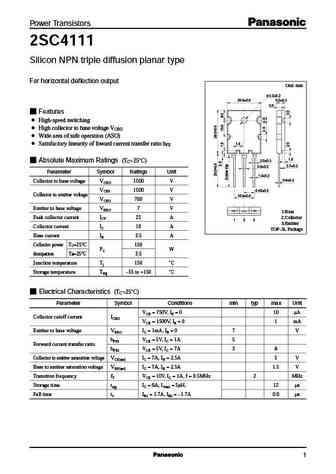
Power Transistors 2SC4111 Silicon NPN triple diffusion planar type For horizontal deflection output Unit mm 3.3 0.2 20.0 0.5 5.0 0.3 3.0 Features High-speed switching High collector to base voltage VCBO Wide area of safe operation (ASO) 1.5 Satisfactory linearity of foward current transfer ratio hFE 1.5 2.0 0.3 Absolute Maximum Ratings (TC=25 C) 2.7 0.3 3.0 0
ut4411.pdf
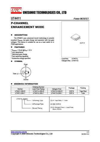
UNISONIC TECHNOLOGIES CO., LTD UT4411 Power MOSFET P-CHANNEL ENHANCEMENT MODE DESCRIPTION The UT4411 uses advanced trench technology to provide excellent RDS(ON), low gate charge and operation with low gate voltages. This device is suitable for use as a load switch or in PWM applications. FEATURES * RDS(ON) = 32m @VGS = 10 V * Low capacitance * Optimized gate char
stc411.pdf
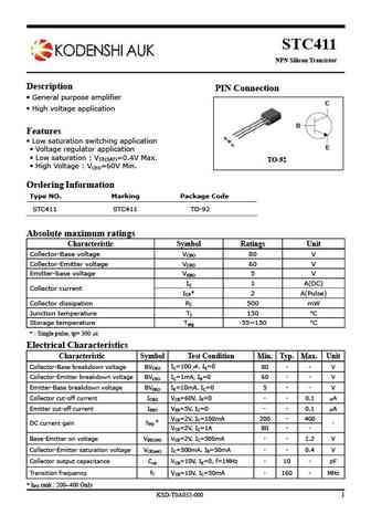
STC411 NPN Silicon Transistor Description PIN Connection General purpose amplifier C High voltage application B Features Low saturation switching application E Voltage regulator application Low saturation VCE(SAT)=0.4V Max. TO-92 High Voltage VCEO=60V Min. Ordering Information Type NO. Marking Package Code STC411 STC411 TO-92 Abso
jansr2n7411.pdf
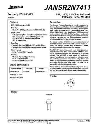
JANSR2N7411 Formerly FSL9110R4 2.5A, -100V, 1.30 Ohm, Rad Hard, June 1998 P-Channel Power MOSFET Features Description 2.5A, -100V, rDS(ON) = 1.30 The Discrete Products Operation of Intersil Corporationhas developed a series of Radiation Hardened MOSFETs specif- Total Dose ically designed for commercial and military space applica- - Meets Pre-RAD Specifications to 100K RAD (Si
mg9411-r.pdf
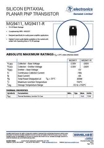
SILICON EPITAXIAL PLANAR PNP TRANSISTOR MG9411, MG9411-R TO-3P Plastic Package Complimentary NPN MG6331 Designed specifically for audio power amplifier applications Highest Current audio bipolar available on the market with widest Safe Operating Area in TO-3P package ABSOLUTE MAXIMUM RATINGS (TA = 25 C unless otherwise stated) MG9411 MG9411-R VCBO Col
2n4114.pdf
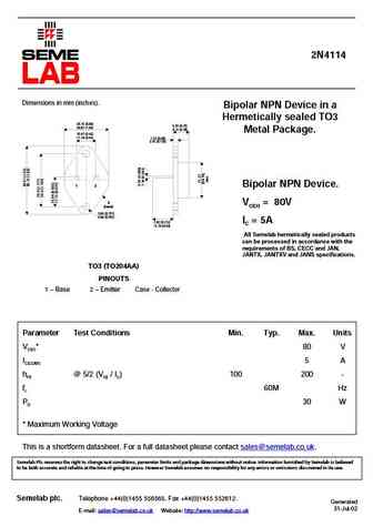
2N4114 Dimensions in mm (inches). Bipolar NPN Device in a Hermetically sealed TO3 25.15 (0.99) 6.35 (0.25) 26.67 (1.05) 9.15 (0.36) Metal Package. 10.67 (0.42) 11.18 (0.44) 1.52 (0.06) 3.43 (0.135) 1 2 Bipolar NPN Device. 3 VCEO = 80V (case) 3.84 (0.151) 4.09 (0.161) 7.92 (0.312) IC = 5A 12.70 (0.50) All Semelab hermetically sealed products can be processed in ac
2n4113.pdf
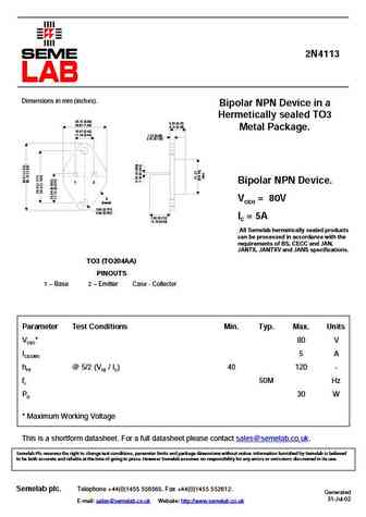
2N4113 Dimensions in mm (inches). Bipolar NPN Device in a Hermetically sealed TO3 25.15 (0.99) 6.35 (0.25) 26.67 (1.05) 9.15 (0.36) Metal Package. 10.67 (0.42) 11.18 (0.44) 1.52 (0.06) 3.43 (0.135) 1 2 Bipolar NPN Device. 3 VCEO = 80V (case) 3.84 (0.151) 4.09 (0.161) 7.92 (0.312) IC = 5A 12.70 (0.50) All Semelab hermetically sealed products can be processed in ac
2n2411x.pdf
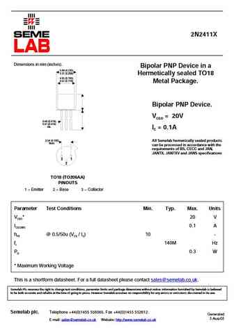
2N2411X Dimensions in mm (inches). Bipolar PNP Device in a 5.84 (0.230) 5.31 (0.209) Hermetically sealed TO18 4.95 (0.195) 4.52 (0.178) Metal Package. Bipolar PNP Device. VCEO = 20V 0.48 (0.019) 0.41 (0.016) dia. IC = 0.1A 2.54 (0.100) All Semelab hermetically sealed products Nom. can be processed in accordance with the requirements of BS, CECC and JAN, JANTX, JA
ssp7411p.pdf
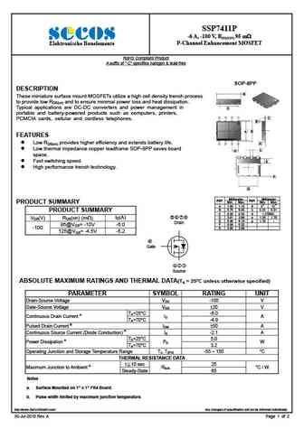
SSP7411P -6 A, -100 V, RDS(ON) 95 m P-Channel Enhancement MOSFET Elektronische Bauelemente RoHS Compliant Product A suffix of -C specifies halogen & lead-free SOP-8PP DESCRIPTION B These miniature surface mount MOSFETs utilize a high cell density trench process to provide low RDS(on) and to ensure minimal power loss and heat dissipation. Typical applications are DC-
2sc2411.pdf
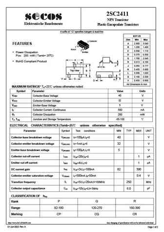
2SC2411 NPN Transistor Elektronische Bauelemente Plastic-Encapsulate Transistors A suffix of "-C" specifies halogen & lead-free SOT-23 Dim Min Max Collector 3 A 2.800 3.040 FEATURES 1 B 1.200 1.400 Base 2 C 0.890 1.110 n Emitter Power Dissipation o D 0.370 0.500 PCM 200 mW ( Tamb= 25 C) G 1.780 2.040 A n RoHS Compliant Product H 0.013 0.100 L J J 0.085 0.
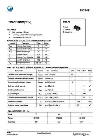
2sc4115.pdf
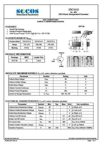
2SC4115 3A , 40V NPN Plastic Encapsulated Transistor Elektronische Bauelemente RoHS Compliant Product A suffix of -C specifies halogen & lead-free SOT-89 FEATURES Small Flat Package 4 General Purpose Application Low VCE(sat).VCE(sat) = 0.2V (Typ.)(IC / IB = 2A / 0.1A) 1 2 3 B C A E CLASSIFICATION OF hFE(1) E C Product-Rank 2SC4115-Q 2SC4115-R 2SC411
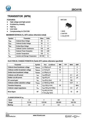
2sc4116.pdf
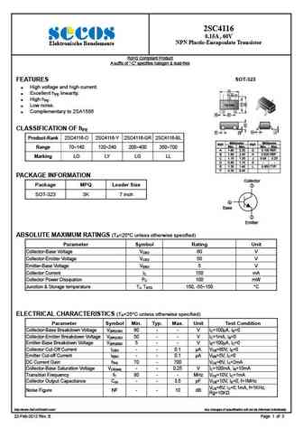
2SC4116 0.15A , 60V NPN Plastic-Encapsulate Transistor Elektronische Bauelemente RoHS Compliant Product A suffix of -C specifies halogen & lead-free SOT-323 FEATURES High voltage and high current. A Excellent hFE linearity. L 3 High hFE. 3 Top View C B Low noise. 1 1 2 Complementary to 2SA1586 2 K E D CLASSIFICATION OF hFE H J F G P
tsc2411cx.pdf
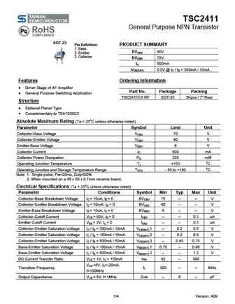
TSC2411 General Purpose NPN Transistor SOT-23 Pin Definition PRODUCT SUMMARY 1. Base BVCEO 40V 2. Emitter 3. Collector BVCBO 75V IC 600mA VCE(SAT) 0.5V @ IC / IB = 380mA / 10mA Features Ordering Information Driver Stage of AF Amplifier Part No. Package Packing General Purpose Switching Application TSC2411CX RF SOT-23 3Kpcs / 7 Reel Structure Ep
csd16411q3.pdf
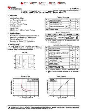
Sample & Support & Product Technical Tools & Buy Community Folder Documents Software CSD16411Q3 SLPS206B AUGUST 2009 REVISED NOVEMBER 2016 CSD16411Q3 25-V N-Channel NexFET Power MOSFET 1 Features Product Summary 1 Ultra-Low Qg and Qgd TA = 25 C TYPICAL VALUE UNIT Low-Thermal Resistance VDS Drain-to-Source Voltage 25 V Avalanche Rated Qg Gate Charge Total (4
tgf4118-epu.pdf
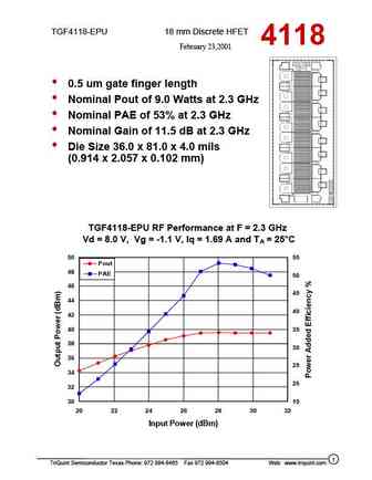
TGF4118-EPU 18 mm Discrete HFET 4118 February 23,2001 0.5 um gate finger length Nominal Pout of 9.0 Watts at 2.3 GHz Nominal PAE of 53% at 2.3 GHz Nominal Gain of 11.5 dB at 2.3 GHz Die Size 36.0 x 81.0 x 4.0 mils (0.914 x 2.057 x 0.102 mm) TGF4118-EPU RF Performance at F = 2.3 GHz Vd = 8.0 V, Vg = -1.1 V, Iq = 1.69 A and TA = 25 C 50 55 Pout 48 PAE 50 46
2n4117 2n4118 2n4119 pn4117 pn4118 pn4119 sst4117 sst4118 sst4119.pdf
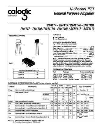
N-Channel JFET General Purpose Amplifier CORPORATION 2N4117 2N4119 / 2N4117A 2N4119A PN4117 PN4119 / PN4117A PN4119A / SST4117 SST4119 FEATURES PIN CONFIGURATION Low Leakage Low Capacitance ABSOLUTE MAXIMUM RATINGS TO-92 (T = 25oC unless otherwise noted) A TO-72 Gate-Source or Gate-Drain Voltage . . . . . . . . . . . . . . . . -40V Gate Curre
csc4115.pdf
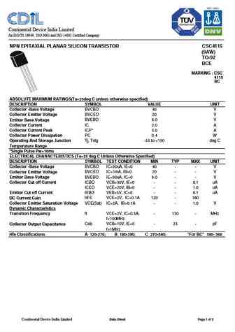
Continental Device India Limited An ISO/TS 16949, ISO 9001 and ISO 14001 Certified Company NPN EPITAXIAL PLANAR SILICON TRANSISTOR CSC4115 (9AW) TO-92 BCE MARKING CSC 4115 BC ABSOLUTE MAXIMUM RATINGS(Ta=25deg C unless otherwise specified) DESCRIPTION SYMBOL VALUE UNIT Collector -Base Voltage BVCBO 40 V Collector Emitter Voltage BVCEO 20 V Emitter Base Voltage BVEBO 6.0 V Collect
2sc2411.pdf
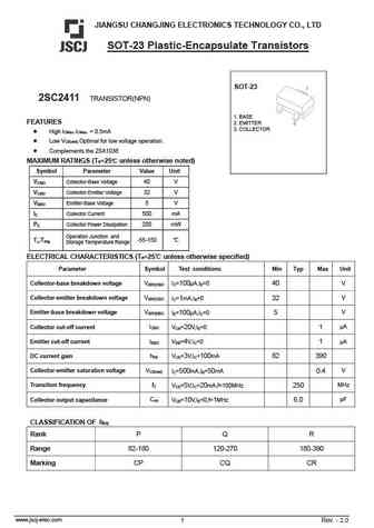
JIANGSU CHANGJING ELECTRONICS TECHNOLOGY CO., LTD SOT-23 Plastic-Encapsulate Transistors SOT-23 2SC2411 TRANSISTOR(NPN) 1. BASE FEATURES 2. EMITTER 3. COLLECTOR High ICMax.ICMax. = 0.5mA Low VCE(sat).Optimal for low voltage operation. Complements the 2SA1036 MAXIMUM RATINGS (Ta=25 unless otherwise noted) Symbol Parameter Value Unit VCBO Collector-Base Voltage 40 V VCE
2sc4115.pdf
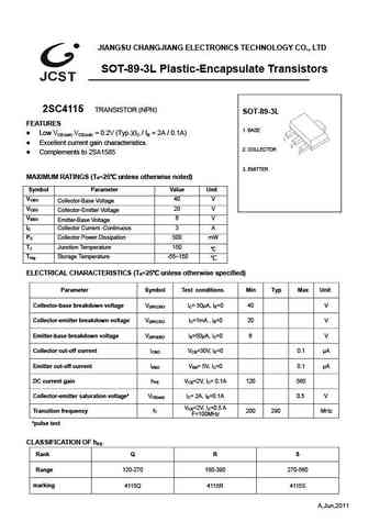
JIANGSU CHANGJIANG ELECTRONICS TECHNOLOGY CO., LTD SOT-89-3L Plastic-Encapsulate Transistors 2SC4115 TRANSISTOR (NPN) SOT-89-3L FEATURES 1. BASE Low VCE(sat).VCE(sat) = 0.2V (Typ.)(IC / IB = 2A / 0.1A) 1 Excellent current gain characteristics. 2 2. COLLECTOR Complements to 2SA1585 3 3. EMITTER MAXIMUM RATINGS (Ta=25 unless otherwise noted) Symbol Parameter
2sc4115s.pdf
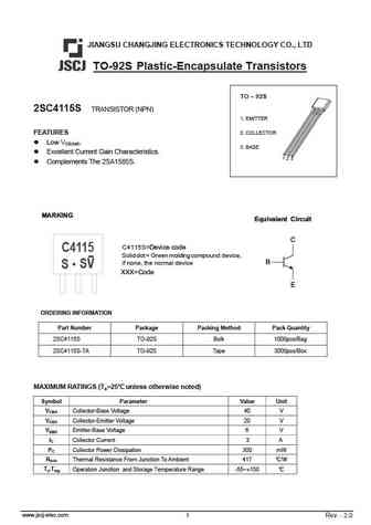
JIANGSU CHANGJING ELECTRONICS TECHNOLOGY CO., LTD TO-92S Plastic-Encapsulate Transistors TO 92S 2SC4115S TRANSISTOR (NPN) 1. EMITTER FEATURES 2. COLLECTOR Low VCE(sat). 3. BASE Excellent Current Gain Characteristics. 1 2 3 Complements The 2SA1585S. Equivalent Circuit C4115S=Device code C4115 Solid dot = Green molding compound device, - if none, the norma
2sc4116.pdf
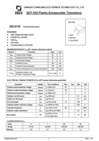
JIANGSU CHANGJING ELECTRONICS TECHNOLOGY CO., LTD SOT-323 Plastic-Encapsulate Transistors SOT-323 2SC4116 TRANSISTOR (NPN) FEATURES High voltage and high current 1. BASE Excellent hFE linearity 2. EMITTER High hFE 3. COLLECTOR Low noise Complementary to 2SA1586 MAXIMUM RATINGS (Ta=25 unless otherwise noted) Symbol Parameter Value Unit V Collector-Base Voltage 60 V
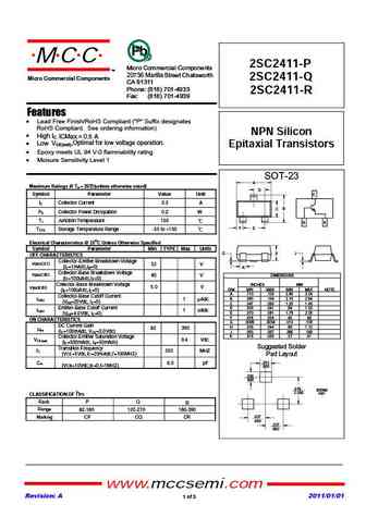
krc410-krc411-krc414.pdf
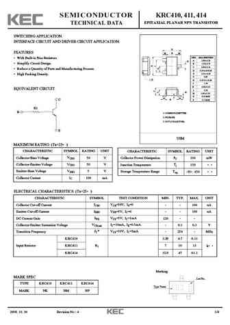
SEMICONDUCTOR KRC410, 411, 414 EPITAXIAL PLANAR NPN TRANSISTOR TECHNICAL DATA SWITCHING APPLICATION. INTERFACE CIRCUIT AND DRIVER CIRCUIT APPLICATION. E FEATURES M B M DIM MILLIMETERS With Built-in Bias Resistors. _ + A 2.00 0.20 D 2 _ Simplify Circuit Design. B 1.25 0.15 + _ + C 0.90 0.10 3 Reduce a Quantity of Parts and Manufacturing Process. 1 D 0.3+0.10/-0.05
ktx411t.pdf
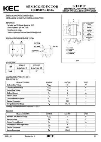
KTX411T SEMICONDUCTOR EPITAXIAL PLANAR NPN TRANSISTOR TECHNICAL DATA SILICON EPITAXIAL PLANAR TYPE DIODE GENERAL PURPOSE APPLICATION. ULTRA HIGH SPEED SWITCHING APPLICATION. E B FEATURES DIM MILLIMETERS _ A 2.9 + 0.2 15 Including two(TR, Diode) devices in TSV. B 1.6+0.2/-0.1 _ C 0.70 + 0.05 (Thin Super Mini type with 5 pin) 2 _ D 0.4 + 0.1 Simplify circuit design. E 2.8+0
ktd1411.pdf
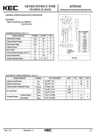
SEMICONDUCTOR KTD1411 TECHNICAL DATA EPITAXIAL PLANAR NPN TRANSISTOR GENERAL PURPOSE DARLINGTON TRANSISTOR. A B D C FEATURES E High DC Current Gain hFE=3000(Min.) F (VCE=2V, IC=1A) G H DIM MILLIMETERS J A 8.3 MAX MAXIMUM RATING (Ta=25 ) K B 5.8 L C 0.7 CHARACTERISTIC SYMBOL RATING UNIT _ + D 3.2 0.1 E 3.5 VCBO Collector-Base Voltage 80 V _ + F 11.0 0.3 G 2.9
2sc2411.pdf
2SC2411 SOT-23 TRANSISOR(NPN) 1. BASE 2. EMITTER FEATURES High ICMax.ICMax. = 0.5mA 3. COLLECTOR Low VCE(sat).Optimal for low voltage operation. Complements the 2SA1036 MAXIMUM RATINGS (TA=25 unless otherwise noted) Symbol Parameter Value Units VCBO Collector-Base Voltage 40 V VCEO Collector-Emitter Voltage 32 V VEBO Emitter-Base Voltage 5 V Collector Current
2sc4115.pdf
2SC4115 TRANSISTOR (NPN) SOT-89 FEATURES Low VCE(sat).VCE(sat) = 0.2V (Typ.)(IC / IB = 2A / 0.1A) 1. BASE 1 Excellent current gain characteristics. 2 Complements to 2SA1585 2. COLLECTOR 3 MAXIMUM RATINGS (TA=25 unless otherwise noted) 3. EMITTER Symbol Parameter Value Units VCBO 40 V Collector-Base Voltage VCEO 20 V Collector-Emitter Voltage VEBO 6 V
2sc4116.pdf
2SC4116 TRANSISTOR (NPN) SOT-323 FEATURES High voltage and high current Excellent hFE linearity High hFE Low noise 1. BASE Complementary to 2SA1586 2. EMITTER MAXIMUM RATINGS (TA=25 unless otherwise noted) 3. COLLECTOR Symbol Parameter Value Units VCBO Collector-Base Voltage 60 V VCEO Collector-Emitter Voltage 50 V VEBO Emitter-Base Voltage 5 V IC Coll
gm6411.pdf
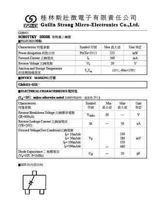
Guilin Strong Micro-Electronics Co.,Ltd. Guilin Strong Micro-Electronics Co.,Ltd. Guilin Strong Micro-Electronics Co.,Ltd. GM6411 SCHOTTKY DIODE SCHOTTKY DIODE SCHOTTKY DIODE FEATURES Characteristic Symbol Max Unit Power dissipation PD(Ta=25 ) 225 mW Fo
2sc2411 sot-23.pdf
2SC2411 SOT-23 Transistor(NPN) 1. BASE SOT-23 2. EMITTER 3. COLLECTOR Features High ICMax.ICMax. = 0.5mA Low VCE(sat).Optimal for low voltage operation. Complements the 2SA1036 MAXIMUM RATINGS (TA=25 unless otherwise noted) Symbol Parameter Value Units VCBO Collector-Base Voltage 40 V Dimensions in inches and (millimeters) VCEO Collector-Emitter Voltage 32
2sc4115.pdf
2SC4115 SOT-89 Transistor(NPN) 1. BASE SOT-89 2. COLLECTOR 1 4.6 B 4.4 1.6 1.8 2 1.4 1.4 3. EMITTER 3 2.6 4.25 2.4 3.75 Features 0.8 MIN 0.53 Low VCE(sat).VCE(sat) = 0.2V (Typ.)(IC / IB = 2A / 0.1A) 0.40 0.48 0.44 2x) 0.13 B 0.35 0.37 Excellent current gain characteristics. 1.5 3.0 Complements to 2SA1585 Dimensions in inches and (millimeter
2sc4116 sot-323.pdf
2SC4116 SOT-323 Transistor(NPN) SOT-323 1. BASE 2. EMITTER 3. COLLECTOR Features High voltage and high current Excellent hFE linearity High hFE Low noise Complementary to 2SA1586 Dimensions in inches and (millimeters) MAXIMUM RATINGS (TA=25 unless otherwise noted) Symbol Parameter Value Units VCBO Collector-Base Voltage 60 V VCEO Collector-Emitter Voltage 50
2sc2411k.pdf
2SC2411K NPN General Purpose Transistors 3 1 P b Lead(Pb)-Free 2 SOT-23 MAXIMUM RATINGS(Ta=25 C) Rating Symbol Value Unit Collector-Emitter Voltage VCEO 32 V VCBO Collector-Base Voltage 40 V VEBO Emitter-Base Voltage 5.0 V IC Collector Current - Continuous 500 mA Total Device Dissipation PD 200 mW TA=25 C Tj C Junction Temperature +150 Tstg Storage Temperature -55 t
2sc4116.pdf
2SC4116 General Purpose Transistor COLLECTOR 3 3 NPN Silicon P b Lead(Pb)-Free 1 1 2 BASE 2 SOT-323(SC-70) FEATURES EMITTER * High voltage and high current * Excellent hFE linearity * High hFE * Low noise * Complementary to 2SA1586 MAXIMUM RATINGS (TA=25 unless otherwise noted) Parameter Symbol Value Units Collector-Base Voltage VCBO 60 V Collector-Emitter Voltage
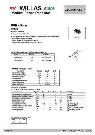
2sc2411kxlt1.pdf
FM120-M WILLAS 2SC2411KxLT1 THRU Medium Power Transistor FM1200-M 1.0A SURFACE MOUNT SCHOTTKY BARRIER RECTIFIERS -20V- 200V SOD-123 PACKAGE Pb Free Product Package outline Features Batch process design, excellent power dissipation offers better reverse leakage current and thermal resistance. SOD-123H Low profile surface mounted application in order to NPN silicon
ao4411.pdf
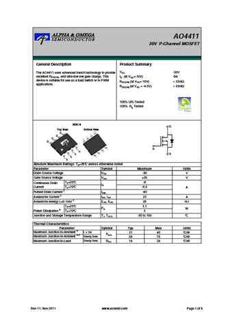
AO4411 30V P-Channel MOSFET General Description Product Summary VDS -30V The AO4411 uses advanced trench technology to provide excellent RDS(ON), and ultra-low low gate charge. This ID (at VGS=-10V) -8A device is suitable for use as a load switch or in PWM RDS(ON) (at VGS=-10V)
ao7411.pdf
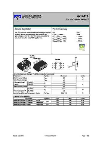
AO7411 20V P-Channel MOSFET General Description Product Summary VDS -20V The AO7411 uses advanced trench technology to provide excellent RDS(ON), low gate charge and operation with ID (at VGS=-4.5V) -1.8A gate voltages as low as 1.8V. This device is suitable for RDS(ON) (at VGS=-4.5V)
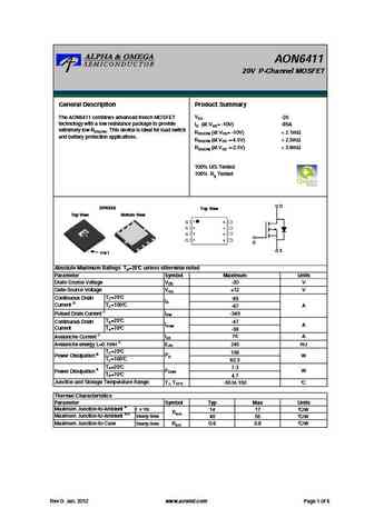
aon2411.pdf
AON2411 12V P-Channel MOSFET General Description Product Summary VDS Latest Trench Power MOSFET technology -12V Very Low RDS(ON) at 1.8V VGS ID (at VGS=-4.5V) -20A Low Gate Charge RDS(ON) (at VGS=-4.5V)
aob411l.pdf
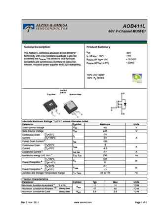
AOB411L 60V P-Channel MOSFET General Description Product Summary VDS The AOB411L combines advanced trench MOSFET -60V -78A technology with a low resistance package to provide ID (at VGS=-10V) extremely low RDS(ON).This device is ideal for boost
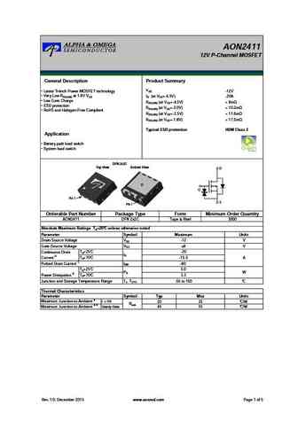
aon6411.pdf
AON6411 20V P-Channel MOSFET General Description Product Summary VDS -20 The AON6411 combines advanced trench MOSFET technology with a low resistance package to provide ID (at VGS= -10V) -85A extremely low RDS(ON). This device is ideal for load switch RDS(ON) (at VGS= -10V)
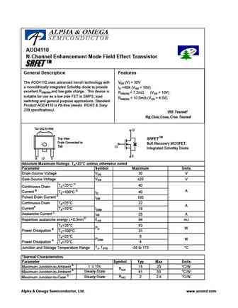
aod4112.pdf
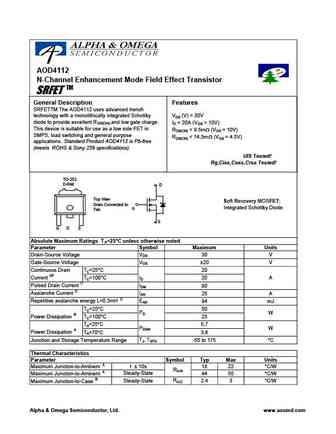
AOD4112 N-Channel Enhancement Mode Field Effect Transistor SRFET TM General Description Features SRFETTM The AOD4112 uses advanced trench technology with a monolithically integrated Schottky VDS (V) = 30V diode to provide excellent R ,and low gate charge. ID = 20A (VGS = 10V) DS(ON) This device is suitable for use as a low side FET in RDS(ON)
aoc2411.pdf
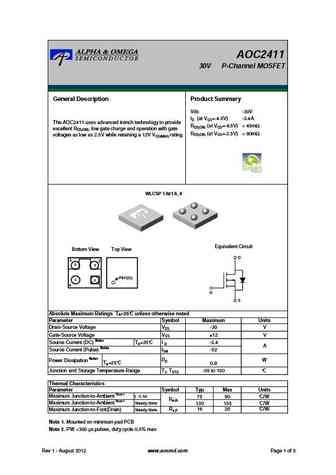
AOC2411 30V P-Channel MOSFET General Description Product Summary Vds -30V ID (at VGS=-4.5V) -3.4A The AOC2411 uses advanced trench technology to provide RDS(ON) (at VGS=-4.5V)
ao6411.pdf
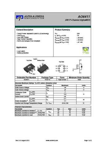
AO6411 20V P-Channel AlphaMOS General Description Product Summary VDS Trench Power AlphaMOS ( MOS LV) technology -20V Low RDS(ON) ID (at VGS=-4.5V) -7A Low Gate Charge RDS(ON) (at VGS=-4.5V)
ap4411gm.pdf
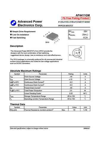
AP4411GM Pb Free Plating Product Advanced Power P-CHANNEL ENHANCEMENT MODE Electronics Corp. POWER MOSFET Simple Drive Requirement BVDSS -30V D D Low On-resistance D RDS(ON) 25m D Fast Switching ID -8.2A G S S SO-8 S Description D The Advanced Power MOSFETs from APEC provide the designer with the best combination of
ap4411gm-hf.pdf
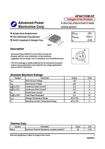
AP4411GM-HF Halogen-Free Product Advanced Power P-CHANNEL ENHANCEMENT MODE Electronics Corp. POWER MOSFET Simple Drive Requirement BVDSS -30V D D D Fast Switching Characteristic RDS(ON) 25m D RoHS Compliant & Halogen-Free ID -8.2A G S S S SO-8 Description D Advanced Power MOSFETs from APEC provide the designer with the best combination of fast switching, rugged
am7411p.pdf
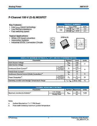
Analog Power AM7411P P-Channel 100-V (D-S) MOSFET PRODUCT SUMMARY Key Features rDS(on) (m ) VDS (V) ID(A) Low r trench technology DS(on) 229 @ VGS = -10V -3.8 Low thermal impedance -100 248 @ VGS = -4.5V -3.7 Fast switching speed Typical Applications DFN5x6-8L White LED boost converters Automotive Systems Industrial DC/DC Conversion Circuits
am6411p.pdf
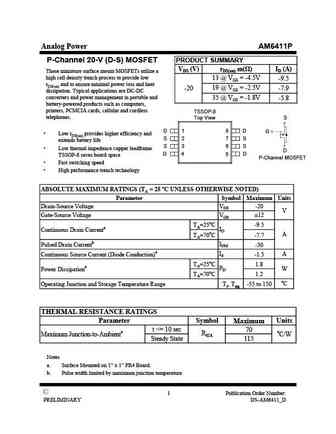
Analog Power AM6411P P-Channel 20-V (D-S) MOSFET PRODUCT SUMMARY VDS (V) rDS(on) m( )ID (A) These miniature surface mount MOSFETs utilize a high cell density trench process to provide low 13 @ VGS = -4.5V -9.5 rDS(on) and to ensure minimal power loss and heat -20 19 @ VGS = -2.5V -7.9 dissipation. Typical applications are DC-DC converters and power management in portable and 35
am3411pe.pdf
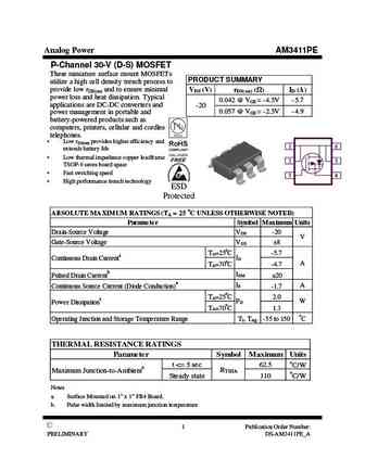
Analog Power AM3411PE P-Channel 30-V (D-S) MOSFET These miniature surface mount MOSFETs PRODUCT SUMMARY utilize a high cell density trench process to provide low rDS(on) and to ensure minimal VDS (V) rDS(on) ( ) ID (A) power loss and heat dissipation. Typical 0.042 @ VGS = -4.5V -5.7 applications are DC-DC converters and -20 0.057 @ VGS = -2.5V -4.9 power management in portab
afp3411.pdf
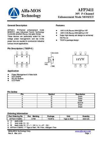
AFP3411 Alfa-MOS 30V P-Channel Technology Enhancement Mode MOSFET General Description Features AFP3411, P-Channel enhancement mode -30V/-6.0A,RDS(ON)=36m @VGS=10V MOSFET, uses Advanced Trench Technology -30V/-4.5A,RDS(ON)=46m @VGS=4.5V to provide excellent RDS(ON), low gate charge. Super high density cell design for extremely These devices are particularly suited
afn8411.pdf
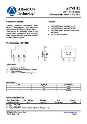
AFN8411 Alfa-MOS 100V N-Channel Technology Enhancement Mode MOSFET General Description Features AFN8411, N-Channel enhancement mode 100V/5.8A,RDS(ON)=115m @VGS=10V MOSFET, uses Advanced Trench Technology 100V/4.6A,RDS(ON)=125m @VGS=4.5V to provide excellent RDS(ON), low gate charge. Super high density cell design for extremely These devices are particularly suited
3dd4110pl.pdf
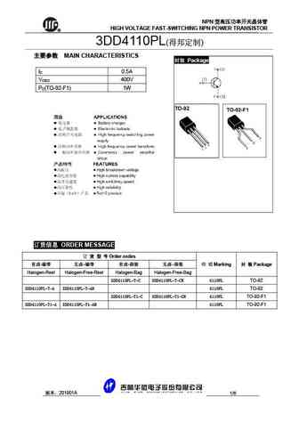
NPN HIGH VOLTAGE FAST-SWITCHING NPN POWER TRANSISTOR R 3DD4110PL( ) MAIN CHARACTERISTICS Package I 0.5A C V 400V CEO P (TO-92-F1) 1W C ORDER MESSAGE Order codes - - - - Marking Package Halogen-Reel Halogen-Free-Reel
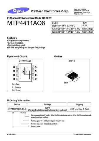
mtp4411q8.pdf
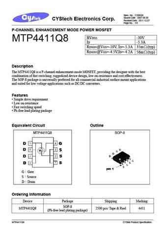
Spec. No. C386Q8 Issued Date 2007.06.08 CYStech Electronics Corp. Revised Date 2011.12.07 Page No. 1/8 P-CHANNEL ENHANCEMENT MODE POWER MOSFET BVDSS -30V MTP4411Q8 ID -5.3A RDSON@VGS=-10V, ID=-5.3A 35m (typ) RDSON@VGS=-4.5V,ID=-4.2A 56m (typ) Description The MTP4411Q8 is a P-channel enhancement-mode MOSFET, providing the designer with the best combination of fast
btb4110d3.pdf
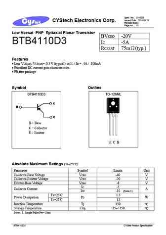
Spec. No. C815D3 Issued Date 2011.03.25 CYStech Electronics Corp. Revised Date Page No. 1/5 Low Vcesat PNP Epitaxial Planar Transistor BVCEO -20V IC -5A BTB4110D3 RCESAT 75m (typ.) Features Low VCE(sat), VCE(sat)=-0.3 V (typical), at IC / IB = -4A / -100mA Excellent DC current gain characteristics Pb-free package Symbol Outline BTB4110D3 TO-126ML
hbn2411s6r.pdf
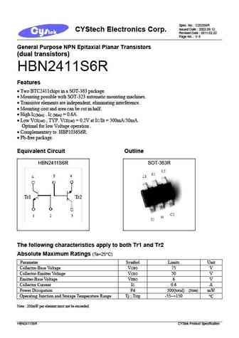
Spec. No. C203S6R Issued Date 2003.09.12 CYStech Electronics Corp. Revised Date 2011.02.22 Page No. 1/ 8 General Purpose NPN Epitaxial Planar Transistors (dual transistors) HBN2411S6R Features Two BTC2411chips in a SOT-363 package. Mounting possible with SOT-323 automatic mounting machines. Transistor elements are independent, eliminating interference.
btc2411n3.pdf
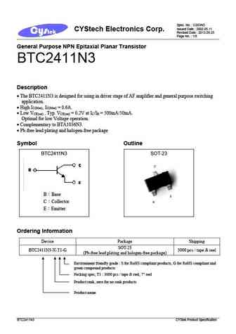
Spec. No. C203N3 Issued Date 2002.05.11 CYStech Electronics Corp. Revised Date 2013.09.25 Page No. 1/8 General Purpose NPN Epitaxial Planar Transistor BTC2411N3 Description The BTC2411N3 is designed for using in driver stage of AF amplifier and general purpose switching application. High I , I = 0.6A. C(Max) C(Max) Low V , Typ. V = 0.2V at I /I = 500mA/
mtp4411aq8.pdf
Spec. No. C386Q8 Issued Date 2007.06.08 CYStech Electronics Corp. Revised Date 2016.03.30 Page No. 1/8 P-Channel Enhancement Mode MOSFET BVDSS -30V MTP4411AQ8 ID@VGS=-10V, TA=25 C -5.3A RDSON@VGS=-10V, ID=-5.3A 30m (typ) RDSON@VGS=-4.5V,ID=-4.2A 43m (typ) Features Simple drive requirement Low on-resistance Fast switching speed Pb-free lead
btc2411l3.pdf
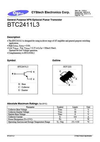
Spec. No. C203L3 Issued Date 2005.02.22 CYStech Electronics Corp. Revised Date 2010.11.12 Page No. 1/8 General Purpose NPN Epitaxial Planar Transistor BTC2411L3 Description The BTC2411L3 is designed for using in driver stage of AF amplifier and general purpose switching application. High I , I = 0.6A. C(Max) C(Max) Low V , Typ. V = 0.2V at I /I = 500mA/
btc2411s3.pdf
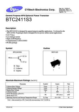
Spec. No. C203S3-R Issued Date 2003.11.18 CYStech Electronics Corp. Revised Date 2010.11.12 Page No. 1/8 General Purpose NPN Epitaxial Planar Transistor BTC2411S3 Description The BTC2411S3 is designed for general purpose amplifier applications. It is housed in the SOT-323/SC-70 package which is designed for low power surface mount applications. Low V CE(sat
btc2411n3g.pdf
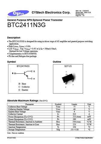
Spec. No. C203N3G Issued Date 2008.12.26 CYStech Electronics Corp. Revised Date Page No. 1/6 General Purpose NPN Epitaxial Planar Transistor BTC2411N3G Description The BTC2411N3G is designed for using in driver stage of AF amplifier and general purpose switching application. High I , I = 0.6A. C(Max) C(Max) Low V , Typ. V = 0.4V at I /I = 500mA/50mA.
mtp4411m3.pdf
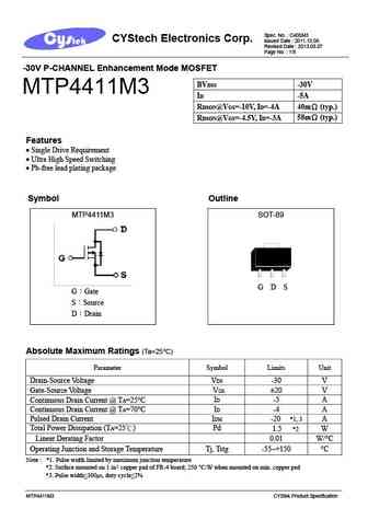
Spec. No. C400M3 CYStech Electronics Corp. Issued Date 2011.10.06 Revised Date 2013.08.07 Page No. 1/8 -30V P-CHANNEL Enhancement Mode MOSFET BVDSS -30V MTP4411M3 ID -5A 40m (typ.) RDSON@VGS=-10V, ID=-4A 58m (typ.) RDSON@VGS=-4.5V, ID=-3A Features Single Drive Requirement Ultra High Speed Switching Pb-free lead plating package Symbol Outline
apm4115pu.pdf
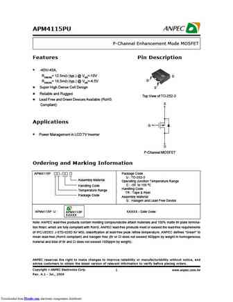
APM4115PU P-Channel Enhancement Mode MOSFET Features Pin Description -40V/-45A, RDS(ON)= 12.5m (typ.) @ VGS=-10V D G RDS(ON)= 18.5m (typ.) @ VGS=-4.5V Super High Dense Cell Design S Reliable and Rugged Top View of TO-252-3 Lead Free and Green Devices Available (RoHS S Compliant) Applications G Power Management in LCD TV Inverter D P-Channel MOSFET Orderin
stu411d.pdf
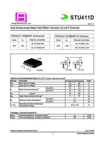
Green Product STU411D a S mHop Microelectronics C orp. Ver 1.1 Dual Enhancement Mode Field Effect Transistor (N and P Channel) PRODUCT SUMMARY (N-Channel) PRODUCT SUMMARY (P-Channel) RDS(ON) (m ) Max RDS(ON) (m ) Max VDSS ID VDSS ID 32 @ VGS=10V 48 @ VGS=-10V 40V 15A -40V -12A 42 @ VGS=4.5V 68 @ VGS=-4.5V D1 D2 D1/D2 G 1 G 2 S 1 G1 S 2 G2 S 1 N-ch S 2 P-ch TO-252-4L (
sts3411a.pdf
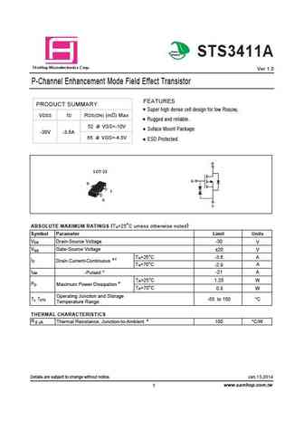
Green Product STS3411A a S mHop Microelectronics C orp. Ver 1.0 P-Channel Enhancement Mode Field Effect Transistor FEATURES PRODUCT SUMMARY Super high dense cell design for low RDS(ON). VDSS ID RDS(ON) (m ) Max Rugged and reliable. 52 @ VGS=-10V Suface Mount Package. -30V -3.6A 65 @ VGS=-4.5V ESD Protected. D SOT-23 G D S G S ABSOLUTE MAXIMUM RATINGS (TA=25 C unless
brcs3411mf.pdf
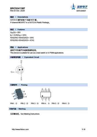
BRCS3411MF Rev.B Oct.-2020 DATA SHEET / Descriptions SOT23-6 P MOS P-channel MOSFET in a SOT23-6 Plastic Package / Features V (V)=-30V DS I =-4.2A(V =-10V) D GS RDS(ON)
lp4411et1g.pdf
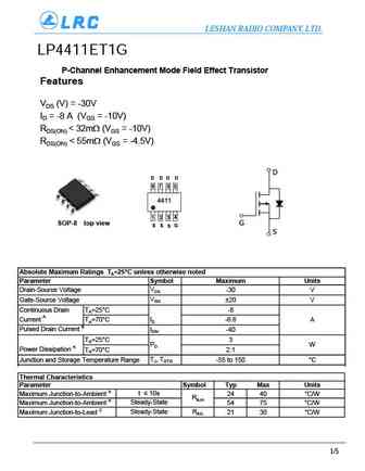
LESHAN RADIO COMPANY, LTD. LP4411ET1G P-Channel Enhancement Mode Field Effect Transistor Features VDS (V) = -30V ID = -8 A (VGS = -10V) RDS(ON)
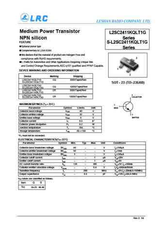
l2sc2411kqlt1g.pdf
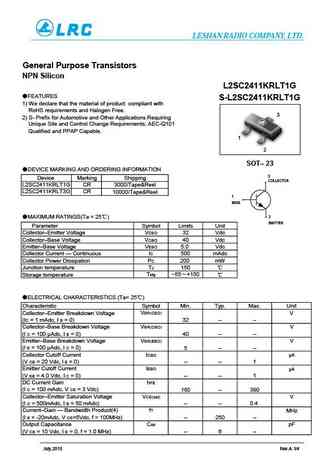
LESHAN RADIO COMPANY, LTD. Medium Power Transistor L2SC2411KQLT1G NPN silicon Series FEATURE S-L2SC2411KQLT1G Epitaxial planar type Series Complementary to L2SA1036K We declare that the material of product are Halogen Free and 3 compliance with RoHS requirements. S- Prefix for Automotive and Other Applications Requiring Unique Site and Control Change Requirements,AEC-q101
l2sc2411krlt1g.pdf
LESHAN RADIO COMPANY, LTD. General Purpose Transistors NPN Silicon L2SC2411KRLT1G FEATURES S-L2SC2411KRLT1G 1) We declare that the material of product compliant with RoHS requirements and Halogen Free. 3 2) S- Prefix for Automotive and Other Applications Requiring Unique Site and Control Change Requirements; AEC-Q101 Qualified and PPAP Capable. 1 2 SOT 23 DEVICE MARK
l2sc2411krlt1g l2sc2411krlt3g.pdf
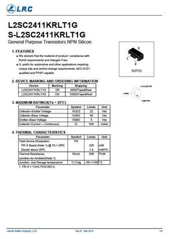
L2SC2411KRLT1G S-L2SC2411KRLT1G General Purpose Transistors NPN Silicon 1. FEATURES We declare that the material of product compliance with RoHS requirements and Halogen Free. S- prefix for automotive and other applications requiring unique site and control change requirements; AEC-Q101 SOT23 qualified and PPAP capable. 2. DEVICE MARKING AND ORDERING INFORMATION Device Mark
2sc4110b.pdf
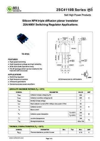
RoHS 2SC4110B Series RoHS SEMICONDUCTOR Nell High Power Products Silicon NPN triple diffusion planar transistor 25A/400V Switching Regulator Applications 15.6 0.4 4.8 0.2 9.6 2.0 0.1 3.2 0,1 TO-3P(B) 2 3 FEATURES +0.2 +0.2 0.65 1.05 -0.1 -0.1 High-speed switching High breakdown voltage and high reliability 5.45 0.1 5.45 0.1 1.4 Wide SOA (Safe Operation Area)
csb4110.pdf
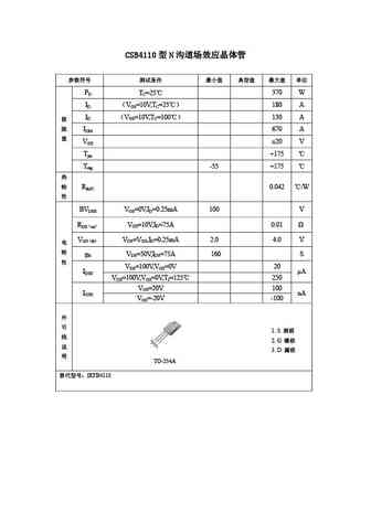
CSB4110 N PD TC=25 370 W ID VGS=10V,TC=25 180 A ID VGS=10V,TC=100 130 A IDM 670 A VGS 20 V Tjm +175 Tstg -55 +175 RthJC 0.042 /W BVDSS VGS=0V,ID=0.25mA 100 V RDS on VGS=10V,ID=75A 0.01 VGS th VDS=VGS,I
ftc2411k.pdf
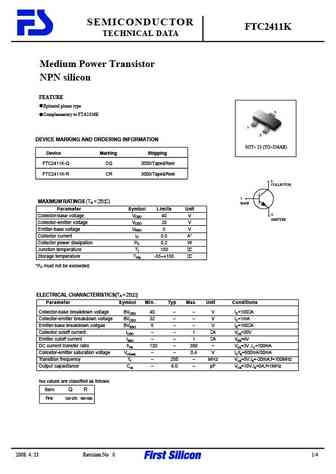
SEMICONDUCTOR FTC2411K TECHNICAL DATA Medium Power Transistor NPN silicon FEATURE Epitaxial planar type 3 Complementary to FTA1036K 1 2 DEVICE MARKING AND ORDERING INFORMATION SOT 23 (TO 236AB) Device Marking Shipping FTC2411K-Q CQ 3000/Tape&Reel FTC2411K-R CR 3000/Tape&Reel 3 COLLECTOR 1 MAXIMUM RATINGS (TA = 25 C) BASE Parameter Symbol Limits Unit 2 Collector-base
dta401-dta411 dta417 dta422-dta423.pdf
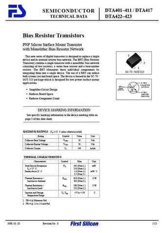
DTA401 411 / DTA417 SEMICONDUCTOR TECHNICAL DATA DTA422 423 Bias Resistor Transistors PNP Silicon Surface Mount Transistor with Monolithic Bias Resistor Network 3 This new series of digital transistors is designed to replace a single device and its external resistor bias network. The BRT (Bias Resistor Transistor) contains a single transistor with a monolithic bias network 2 consisti
2sc4118.pdf
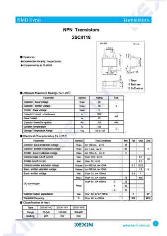
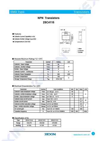
SMD Type Transistors NPN Transistors 2SC4118 Features Excellent hFE linearity hFE(2)=25(min) Complementary to 2SA1588 1 Base 2 Emitter 3 Collector Absolute Maximum Ratings Ta = 25 Parameter Symbol Rating Unit Collector - Base Voltage VCBO 35 Collector - Emitter Voltage VCEO 30 V Emitter - Base Voltage VEBO 5 Collector Current - Continuous IC 500 mA Ba
ao4411.pdf
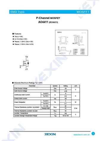
SMD Type MOSFET P-Channel MOSFET AO4411 (KO4411) SOP-8 Features VDS (V) =-30V ID =-8 A (VGS =-10V) RDS(ON) 32m (VGS =-10V) 1.50 0.15 RDS(ON) 55m (VGS =-4.5V) 1 Source 5 Drain 6 Drain 2 Source 7 Drain 3 Source 8 Drain 4 Gate D G S Absolute Maximum Ratings Ta = 25 Parameter Symbol Rating Unit Drain-Source Voltage VDS -30 V Gate-
2sc4117.pdf
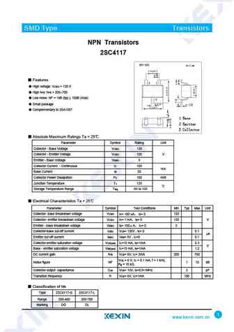
SMD Type Transistors NPN Transistors 2SC4117 Features High voltage VCEO = 120 V High hFE hFE = 200 700 Low noise NF = 1dB (typ.), 10dB (max) Small package Complementary to 2SA1587 1 Base 2 Emitter 3 Collector Absolute Maximum Ratings Ta = 25 Parameter Symbol Rating Unit Collector - Base Voltage VCBO 120 Collector - Emitter Voltage VCEO 120
2sc2411.pdf
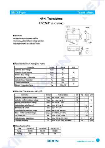
SMD Type Transistors NPN Transistors 2SC2411 (2SC2411K) SOT-23 Unit mm +0.1 2.9-0.1 +0.1 0.4 -0.1 3 Features Collector Current Capability IC=0.5A 1 2 Low VCE(sat).Optimal for low voltage operation. +0.05 0.95+0.1 -0.1 0.1 -0.01 1.9+0.1 -0.1 Complements the 2SA1036/2SA1036K 1.Base 2.Emitter 3.collector Absolute Maximum Ratings Ta = 25 Parameter
2sc4115.pdf
SMD Type Transistors NPN Transistors 2SC4115 1.70 0.1 Features Collector Current Capability IC=3A Collector Emitter Voltage VCEO=20V Complements to 2SA1585 0.42 0.1 0.46 0.1 1.Base 2.Collector 3.Emitter Absolute Maximum Ratings Ta = 25 Parameter Symbol Rating Unit Collector - Base Voltage VCBO 40 Collector - Emitter Voltage VCEO 20 V Emitter - Base
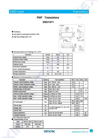
2sa1411.pdf
SMD Type or SMD Type TransistICs PNP Transistors 2SA1411 SOT-23 Unit mm +0.1 2.9 -0.1 +0.1 0.4 -0.1 3 Features Very high DC current gain hFE=500 to 1600. High VEBO Voltage VEBO=-10V 1 2 +0.1 +0.05 0.95-0.1 0.1-0.01 +0.1 1.9-0.1 1.Base 2.Emitter 3.collector Absolute Maximum Ratings Ta = 25 Parameter Symbol Rating Unit Collector-base voltage VCBO -25 V Collector-emitte
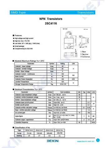
2sc4116.pdf
SMD Type Transistors NPN Transistors 2SC4116 Features High voltage and high current High hFE hFE = 70 700 Low noise NF = 1dB (typ.), 10dB (max) Small package Complementary to 2SA1586 1 Base 2 Emitter 3 Collector Absolute Maximum Ratings Ta = 25 Parameter Symbol Rating Unit Collector - Base Voltage VCBO 60 Collector - Emitter Voltage VCEO 50
2sc2411k.pdf
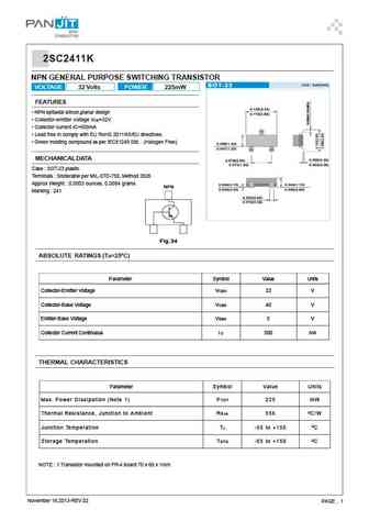
2SC2411K NPN GENERAL PURPOSE SWITCHING TRANSISTOR VOLTAGE 32 Volts POWER 225mW FEATURES 0.120(3.04) NPN epitaxial silicon,planar design 0.110(2.80) Collector-emitter voltage VCE=32V Collector current IC=500mA Lead free in comply with EU RoHS 2011/65/EU directives. Green molding compound as per IEC61249 Std. . (Halogen Free) 0.056(1.40) 0.047(1.20) MECHANICAL DAT
pja3411.pdf
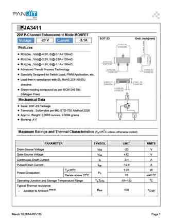
PPJA3411 20V P-Channel Enhancement Mode MOSFET SOT-23 Unit inch(mm) Voltage -20 V Current -3.1A Features RDS(ON) , VGS@-4.5V, ID@-3.1A
2sc2411kgp.pdf
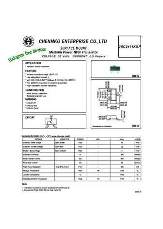
CHENMKO ENTERPRISE CO.,LTD 2SC2411KGP SURFACE MOUNT Medium Power NPN Transistor VOLTAGE 32 Volts CURRENT 0.5 Ampere APPLICATION * Medium Power Amplifier . FEATURE * Surface mount package. (SOT-23) SOT-23 * Low saturation voltage V * Low cob. Cob=6.0pF(Typ.) CE(sat)=0.4V(max.)(IC=500mA) * PC= 200mW (mounted on ceramic substrate). * High saturation current capability. (1) CONST
csd16411q3.pdf
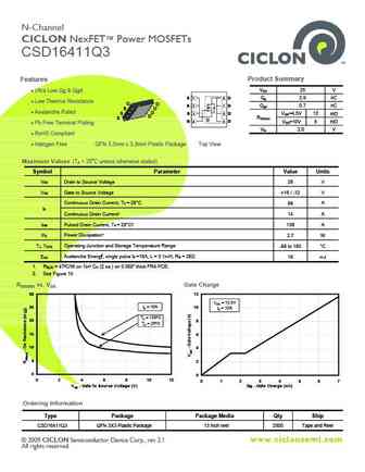
N-Channel CICLON NexFET Power MOSFETs CSD16411Q3 Product Summary Features Ultra Low Qg & Qgd VDS 25 V S 1 8 D S 1 8 D Qg 2.9 nC Low Thermal Resistance G D S 2 7 D S 2 7 D Qgd 0.7 nC S D Avalanche Rated D S S 3 6 D VGS=4.5V 12 m S 3 6 D D RDS(on) S D D G 4 5 D G 4 5 D VGS=10V 8 m Pb Free Terminal Plating Vth 2.0 V RoHS Compli
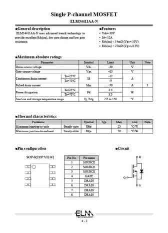
elm14411aa.pdf
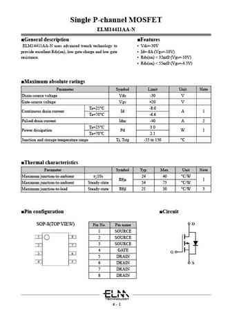
Single P-channel MOSFET ELM14411AA-N General description Features ELM14411AA-N uses advanced trench technology to Vds=-30V provide excellent Rds(on), low gate charge and low gate Id=-8A (Vgs=-10V) resistance. Rds(on)
elm34411aa.pdf
Single P-channel MOSFET ELM34411AA-N General description Features ELM34411AA-N uses advanced trench technology to Vds=-30V provide excellent Rds(on), low gate charge and low gate Id=-12A resistance. Rds(on)
elm33411ca.pdf
Single P-channel MOSFET ELM33411CA-S General description Features ELM33411CA-S uses advanced trench technology to Vds=-20V provide excellent Rds(on), low gate charge and low gate Id=-3A resistance. Rds(on)
gsm8411.pdf
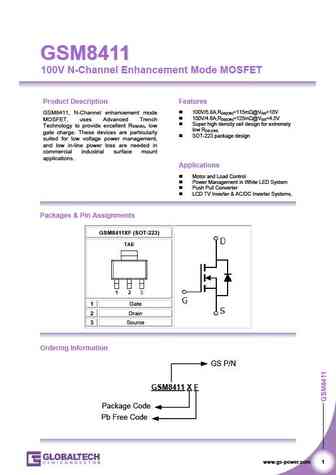
GSM8411 GSM8411 100V N-Channel Enhancement Mode MOSFET Product Description Features 100V/5.8A,RDS(ON)=115m @VGS=10V GSM8411, N-Channel enhancement mode 100V/4.6A,RDS(ON)=125m @VGS=4.5V MOSFET, uses Advanced Trench Super high density cell design for extremely Technology to provide excellent RDS(ON), low low RDS (ON) gate charge. These devices are particularly
gsm3411.pdf
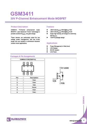
GSM3411 30V P-Channel Enhancement Mode MOSFET Product Description Features GSM3411, P-Channel enhancement mode -30V/-6.0A,RDS(ON)=36m @VGS=10V MOSFET, uses Advanced Trench Technology to -30V/-4.5A,RDS(ON)=46m @VGS=4.5V provide excellent RDS(ON), low gate charge. Super high density cell design for extremely low RDS (ON) These devices are particularly suited for low
3dg4115s.pdf

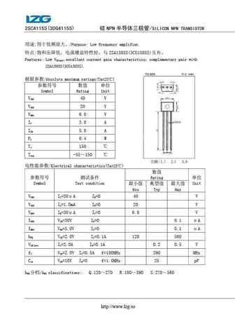
2SC4115S(3DG4115S) NPN /SILICON NPN TRANSISTOR /Purpose Low frequency amplifier. 2SA1585S(3CG1585S) Features Low V ,excellent current gain characteristics complementary pair with CE(sat) 2SA1585S(3CG1585S). /Absolute maximum ratings(Ta=25 )
2sc4115s-r.pdf
2SC4115S(3DG4115S) NPN /SILICON NPN TRANSISTOR /Purpose Low frequency amplifier. 2SA1585S(3CG1585S) Features Low V ,excellent current gain characteristics complementary pair with CE(sat) 2SA1585S(3CG1585S). /Absolute maximum ratings(Ta=25 )
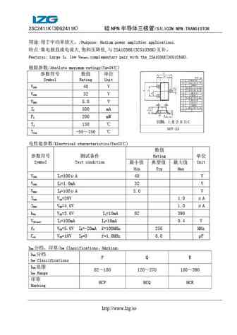
3dg2411k.pdf
2SC2411K(3DG2411K) NPN /SILICON NPN TRANSISTOR /Purpose Medium power amplifier applications. , , 2SA1036K(3CG1036K) Features Large I , low V ,complementary pair with the 2SA1036K(3CG1036K). C CE(sat) /Absolute maximum ratings(Ta=25 )
2sc4115s-s.pdf

2SC4115S(3DG4115S) NPN /SILICON NPN TRANSISTOR /Purpose Low frequency amplifier. 2SA1585S(3CG1585S) Features Low V ,excellent current gain characteristics complementary pair with CE(sat) 2SA1585S(3CG1585S). /Absolute maximum ratings(Ta=25 )
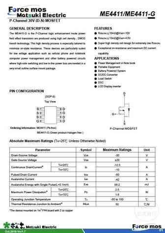
me4411 me4411-g.pdf
ME4411/ME4411-G P-Channel 30V (D-S) MOSFET GENERAL DESCRIPTION FEATURES The ME4411-G is the P-Channel logic enhancement mode power RDS(ON) 10m @VGS=-10V field effect transistors are produced using high cell density , DMOS RDS(ON) 13m @VGS=-4.5V trench technology. This high density process is especially tailored to Super high density cell design for extremely low RD
mmp4411.pdf
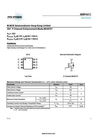
MMP4411 Data Sheet M-MOS Semiconductor Hong Kong Limited 30V P-Channel Enhancement-Mode MOSFET VDS= -30V RDS(ON), Vgs@-10V, Ids@-8A = 32m RDS(ON), Vgs@-4.5V, Ids@-5A = 55m Features Advanced trench process technology High Density Cell Design For Ultra Low On-Resistance SO-8 Internal Schematic Diagram Top View P-Channel MOSFET Maximum Ratings and Thermal Characteristics (TA = 25
mmp4411dy.pdf
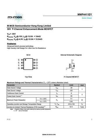
MMP4411DY Data Sheet M-MOS Semiconductor Hong Kong Limited 30V P-Channel Enhancement-Mode MOSFET VDS= -30V RDS(ON), Vgs@-10V, Ids@-13.0A = 10m RDS(ON), Vgs@-4.5V, Ids@-10.0A = 15.5m Features Advanced trench process technology High Density Cell Design For Ultra Low On-Resistance SO-8 Internal Schematic Diagram Top View P-Channel MOSFET Maximum Ratings and Thermal Characteristic
stn4110.pdf
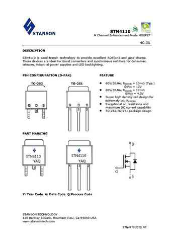
STN4110 N Channel Enhancement Mode MOSFET 40.0A DESCRIPTION STN4110 is used trench technology to provide excellent RDS(on) and gate charge. Those devices are ideal for boost converters and synchronous rectifiers for consumer, telecom, industrial power supplies and LED backlighting. PIN CONFIGURATION (D-PAK) FEATURE 60V/20.0A, RDS(ON) = 10m (Typ.) TO-252 TO-251 @VGS =
2sc4115c.pdf
SUNROC 2SC4115S TRANSISTOR (NPN) TO-92S FEATURES 1. EMITTER Power dissipation PD 0.3 W (Tamb=25 ) 2. COLLECTOR Collector current I CM 3 A 3. BASE Collector-base voltage V(BR)CBO 40 V Operating and storage junction temperature range 123 TJ, Tstg -55 to +150 ELECTRICAL CHARACTERISTICS (Tamb=25 unless otherwise specified) Parameter Sy
tfn2411.pdf
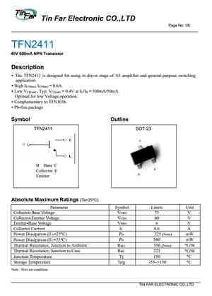
Tin Far Electronic CO.,LTD Page No 2/6 Characteristics (Ta=25 C) Symbol Min. Typ. Max. Unit Test Conditions BV 75 - - V I =10 A CBO C BV 40 - - V I =10mA CEO C BV 6 - - V I =10 A EBO E I - - 10 nA V =60V CBO CB I - - 10 nA V =60V, V =-3V CEX CE BE I - - 10 nA V =3V EBO EB *V 1 - - 0.5 V I =380mA, I =10mA CE(sat) C B *V 2 - - 0.4 V I =150mA, I =15mA CE(sat) C B *
tfh2411.pdf
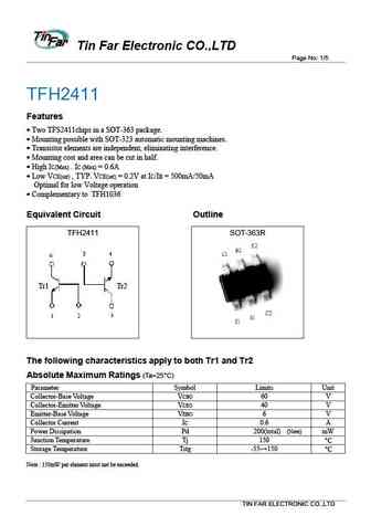
Tin Far Electronic CO.,LTD Page No 1/5 TFH2411 Features Two TFS2411chips in a SOT-363 package. Mounting possible with SOT-323 automatic mounting machines. Transistor elements are independent, eliminating interference. Mounting cost and area can be cut in half. High IC(Max) . IC (Max) = 0.6A Low VCE(sat) , TYP. VCE(sat) = 0.2V at IC/IB = 500mA/50mA O
qm2411j.pdf
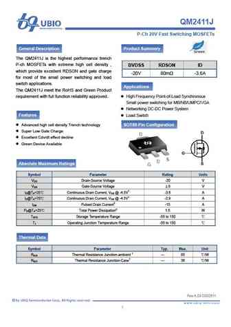
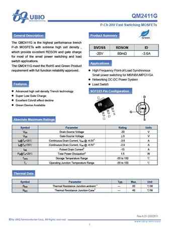
QM2411J P-Ch 20V Fast Switching MOSFETs General Description Product Summery The QM2411J is the highest performance trench P-ch MOSFETs with extreme high cell density , BVDSS RDSON ID which provide excellent RDSON and gate charge -20V 80m -3.6A for most of the small power switching and load switch applications. Applications The QM2411J meet the RoHS and Green Product req
qm2411k.pdf
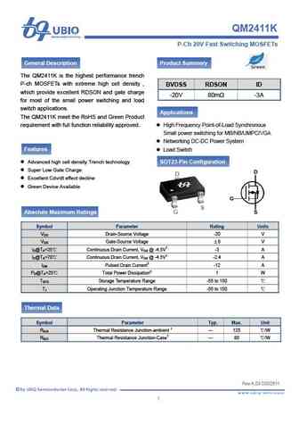
QM2411K P-Ch 20V Fast Switching MOSFETs General Description Product Summery The QM2411K is the highest performance trench P-ch MOSFETs with extreme high cell density , BVDSS RDSON ID which provide excellent RDSON and gate charge -20V 80m -3A for most of the small power switching and load switch applications. Applications The QM2411K meet the RoHS and Green Product requir
qm2411g.pdf
QM2411G P-Ch 20V Fast Switching MOSFETs General Description Product Summery The QM2411G is the highest performance trench P-ch MOSFETs with extreme high cell density , BVDSS RDSON ID which provide excellent RDSON and gate charge -20V 80m -3.6A for most of the small power switching and load switch applications. Applications The QM2411G meet the RoHS and Green Product req
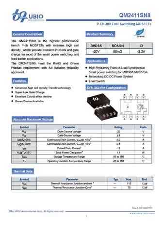
qm2411sn8.pdf
QM2411SN8 P-Ch 20V Fast Switching MOSFETs General Description Product Summery The QM2411SN8 is the highest performance trench P-ch MOSFETs with extreme high cell BVDSS RDSON ID density , which provide excellent RDSON and gate -20V 80m -3.2A charge for most of the small power switching and load switch applications. Applications The QM2411SN8 meet the RoHS and Green Produc
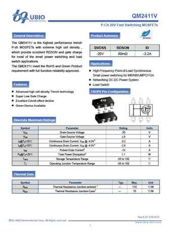
qm2411v.pdf
QM2411V P-Ch 20V Fast Switching MOSFETs General Description Product Summery The QM2411V is the highest performance trench P-ch MOSFETs with extreme high cell density , BVDSS RDSON ID which provide excellent RDSON and gate charge -20V 80m -3.2A for most of the small power switching and load switch applications. Applications The QM2411V meet the RoHS and Green Product requ
hsm4113.pdf
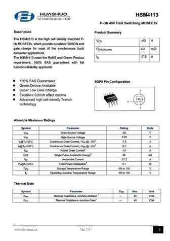
HSM4113 P-Ch 40V Fast Switching MOSFETs Description Product Summary The HSM4113 is the high cell density trenched P- VDS -40 V ch MOSFETs, which provide excellent RDSON and gate charge for most of the synchronous buck RDS(ON),max 40 m converter applications. ID -7.5 A The HSM4113 meet the RoHS and Green Product requirement, 100% EAS guaranteed with full function reli
hsbb4115.pdf
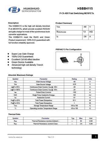
HSBB4115 P-Ch 40V Fast Switching MOSFETs Description Product Summary The HSBB4115 is the high cell density trenched VDS -40 V P-ch MOSFETs, which provide excellent RDSON and gate charge for most of the synchronous buck RDS(ON),max 13 m converter applications. ID -39 A The HSBB4115 meet the RoHS and Green Product requirement, 100% EAS guaranteed with full function relia
hsu4115.pdf
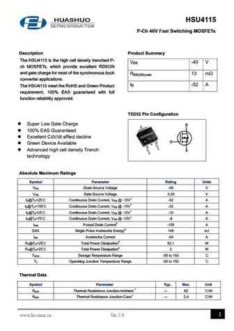
HSU4115 P-Ch 40V Fast Switching MOSFETs Description Product Summary The HSU4115 is the high cell density trenched P- VDS -40 V ch MOSFETs, which provide excellent RDSON and gate charge for most of the synchronous buck RDS(ON),max 13 m converter applications. ID -52 A The HSU4115 meet the RoHS and Green Product requirement, 100% EAS guaranteed with full function reliab
hsu4113.pdf
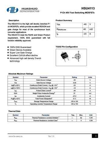
HSU4113 P-Ch 40V Fast Switching MOSFETs Description Product Summary The HSU4113 is the high cell density trenched P- VDS -40 V ch MOSFETs, which provide excellent RDSON and RDS(ON),max 40 m gate charge for most of the synchronous buck converter applications. ID -23 A The HSU4113 meet the RoHS and Green Product requirement, 100% EAS guaranteed with full function reliabil
hsm4115.pdf
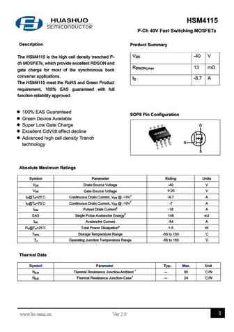
HSM4115 P-Ch 40V Fast Switching MOSFETs Description Product Summary VDS -40 V The HSM4115 is the high cell density trenched P- ch MOSFETs, which provide excellent RDSON and RDS(ON),max 13 m gate charge for most of the synchronous buck converter applications. ID -8.7 A The HSM4115 meet the RoHS and Green Product requirement, 100% EAS guaranteed with full function relia
irfb4110.pdf
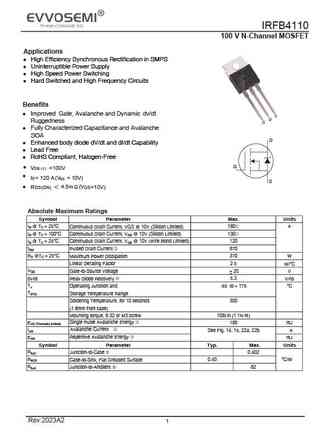
IRFB4110 100 V N-Channel MOSFET Applications l High Efficiency Synchronous Rectification in SMPS l Uninterruptible Power Supply l High Speed Power Switching l Hard Switched and High Frequency Circuits Benefits l Improved Gate, Avalanche and Dynamic dv/dt Ruggedness l Fully Characterized Capacitance and Avalanche SOA D l Enhanced body diode dV/dt and dI/dt Capability l Lead Free l
irfp4110.pdf
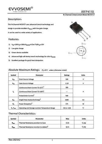
IRFP4110 N-Channel Enhancement Mode MOSFET Electrical Characteristics (TC=25 unless otherwise noted) Symbol Parameter Conditions Min Typ Max Units Off Characteristics Drain-Sourtce Breakdown Voltage VGS=0V,ID=250 A 100 --- --- V BVDSS Zero Gate Voltage Drain Current VGS=0V, VDS=100V --- --- 1 A IDSS Gate-Source Leakage Current IGSS VGS= 20V, VDS=0A --- --- 100 nA On Chara
sm4411.pdf
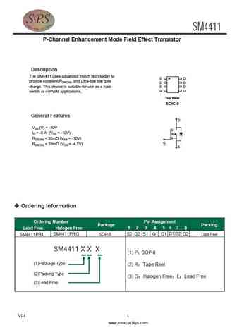
SM4411 P-Channel Enhancement Mode Field Effect Transistor Description The SM4411 uses advanced trench technology to S D provide excellent RDS(ON), and ultra-low low gate S D charge. This device is suitable for use as a load S D G D switch or in PWM applications. Top View SOIC-8 General Features D VDS (V) = -30V ID = -8 A (VGS = -10V) RDS(ON)
2sc4110t4tl.pdf
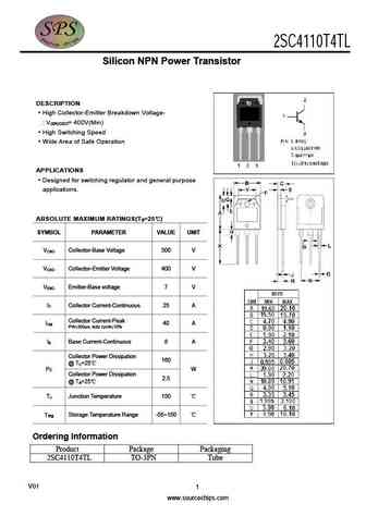
2SC4110T4TL Silicon NPN Power Transistor DESCRIPTION High Collector-Emitter Breakdown Voltage- V = 400V(Min) (BR)CEO High Switching Speed Wide Area of Safe Operation APPLICATIONS Designed for switching regulator and general purpose applications. ABSOLUTE MAXIMUM RATINGS(T =25 ) a SYMBOL PARAMETER VALUE UNIT V Collector-Base Voltage 500 V CBO V Collector-Emitter Volta
ao4411.pdf
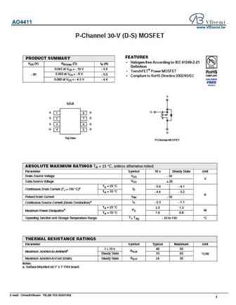
AO4411 www.VBsemi.tw P-Channel 30-V (D-S) MOSFET FEATURES PRODUCT SUMMARY Halogen-free According to IEC 61249-2-21 VDS (V) RDS(on) ( )ID (A) Definition 0.042 at VGS = - 10 V - 5.8 TrenchFET Power MOSFET 0.055 at VGS = - 6 V - 30 - 5.0 Compliant to RoHS Directive 2002/95/EC 0.060 at VGS = - 4.5 V - 4.4 S SO-8 G SD 1 8 S D 2 7 3 6 SD G D 4 5 D Top Vi
irfr3411pbf.pdf
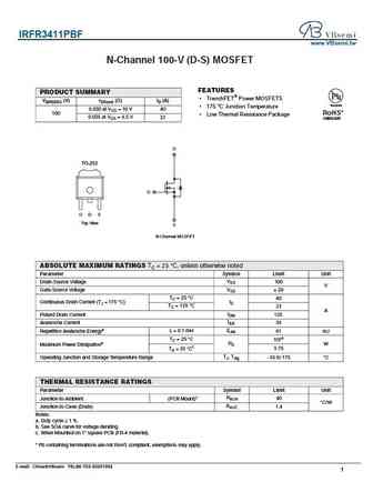
IRFR3411PBF www.VBsemi.tw N-Channel 100-V (D-S) MOSFET FEATURES PRODUCT SUMMARY TrenchFET Power MOSFETS V(BR)DSS (V) rDS(on) ( )ID (A) Available 175 C Junction Temperature 0.030 at VGS = 10 V 40 RoHS* 100 Low Thermal Resistance Package 0.035 at VGS = 4.5 V 37 COMPLIANT D TO-252 G G D S Top View S N-Channel MOSFET ABSOLUTE MAXIMUM RATINGS TC = 25 C, un
irfr3411tr.pdf
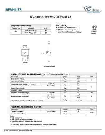
IRFR3411TR www.VBsemi.tw N-Channel 100-V (D-S) MOSFET FEATURES PRODUCT SUMMARY TrenchFET Power MOSFETS V(BR)DSS (V) rDS(on) ( )ID (A) Available 175 C Junction Temperature 0.030 at VGS = 10 V 40 RoHS* 100 Low Thermal Resistance Package 0.035 at VGS = 4.5 V 37 COMPLIANT D TO-252 G G D S Top View S N-Channel MOSFET ABSOLUTE MAXIMUM RATINGS TC = 25 C, unl
ntgs4111pt.pdf
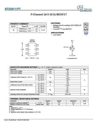
NTGS4111PT www.VBsemi.tw P-Channel 30-V (D-S) MOSFET FEATURES PRODUCT SUMMARY Halogen-free According to IEC 61249-2-21 VDS (V) RDS(on) ( ) ID (A)a Qg (Typ.) Available 0.049 at VGS = - 10 V - 4.8 TrenchFET Power MOSFET - 30 5.1 nC 0.054 at VGS = - 4.5 V - 4.1 APPLICATIONS Load Switch TSOP-6 (4) S Top V iew 1 6 (3) G 3 mm 5 2 3 4 (1, 2, 5, 6) D 2.85 mm P-
aod4112.pdf
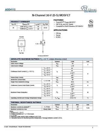
AOD4112 www.VBsemi.tw N-Channel 30-V (D-S) MOSFET FEATURES PRODUCT SUMMARY TrenchFET Power MOSFET VDS (V) RDS(on) ( ) ID (A)a, e Qg (Typ) 100 % Rg and UIS Tested Compliant to RoHS Directive 2011/65/EU 0.007 at VGS = 10 V 50 30 25 nC 0.009 at VGS = 4.5 V 40 APPLICATIONS D OR-ing Server TO-252 DC/DC G G D S S Top View N-Channel MOSFET ABSOLU
hm4110t.pdf
HM4110T N-Channel Enhancement Mode Power MOSFET Description The HM4110T uses advanced trench technology and design to provide excellent RDS(ON) with low gate charge. It can be used in a wide variety of other applications. General Features VDSS =100V,ID =210A RDS(ON)
hms4110t.pdf
HMS4110T N-Channel Super Trench Power MOSFET Description The HMS4110T uses Super Trench technology that is uniquely optimized to provide the most efficient high frequency switching performance. Both conduction and switching power losses are minimized due to an extremely low combination of RDS(ON) and Qg. This device is ideal for high-frequency switching and synchronous rectificat
hm4110.pdf
100VDS 25VGS 170A(ID) N-Channel Enha ncement Mode MOSFET Features Pin Description VDSS= 0V VGSS= 25V ID=1 0A RDS(ON)=5 m (max.)@VGS=10V Low Dense Cell Design Reliable and Rugged Advanced trench process technology Applications Synchronous Rectification Power Manage
irfb4110.pdf
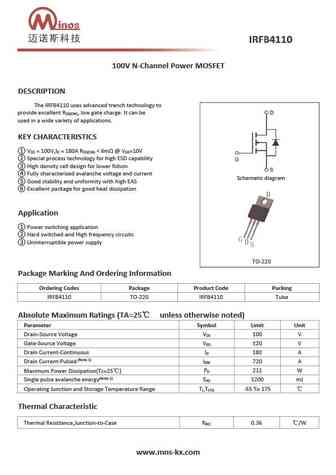
100V N-Channel Power MOSFET DESCRIPTION The IRFB4110 uses advanced trench technology to provide excellent R , low gate charge. It can be DS(ON) used in a wide variety of applications. KEY CHARACTERISTICS V = 100V,I = 180A R
2sc4110l 2sc4110m 2sc4110n.pdf
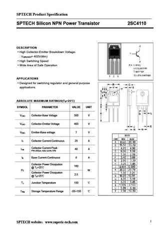
SPTECH Product Specification SPTECH Silicon NPN Power Transistor 2SC4110 DESCRIPTION High Collector-Emitter Breakdown Voltage- V = 400V(Min) (BR)CEO High Switching Speed Wide Area of Safe Operation APPLICATIONS Designed for switching regulator and general purpose applications. ABSOLUTE MAXIMUM RATINGS(T =25 ) a SYMBOL PARAMETER VALUE UNIT V Collector-Base Voltage 500 V
irfb4115g.pdf
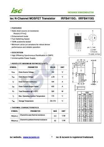
isc N-Channel MOSFET Transistor IRFB4115G IIRFB4115G FEATURES Static drain-source on-resistance RDS(on) 11m Enhancement mode Fast Switching Speed 100% avalanche tested Minimum Lot-to-Lot variations for robust device performance and reliable operation DESCRITION High Efficiency Synchronous Rectification in SMPS Uninterruptible Power Supply ABSOLUTE MAXIMU
2n4112.pdf

isc Silicon NPN Power Transistor 2N4112 DESCRIPTION Excellent Safe Operating Area Low Collector-Emitter Saturation Voltage 100% avalanche tested Minimum Lot-to-Lot variations for robust device performance and reliable operation. APPLICATIONS Designed for general-purpose switching and amplifier applications ABSOLUTE MAXIMUM RATINGS(T =25 ) a SYMBOL PARAMETER VALUE UNIT V
2sk4115.pdf
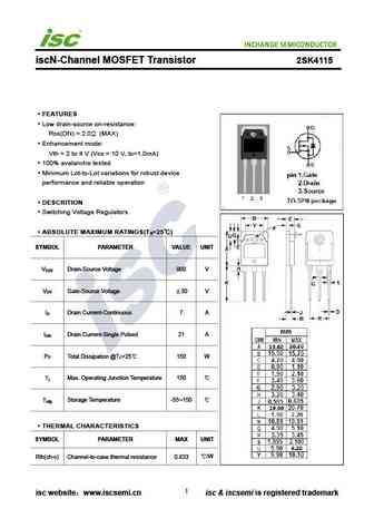
iscN-Channel MOSFET Transistor 2SK4115 FEATURES Low drain-source on-resistance RDS(ON) = 2.0 (MAX) Enhancement mode Vth = 2 to 4 V (VDS = 10 V, ID=1.0mA) 100% avalanche tested Minimum Lot-to-Lot variations for robust device performance and reliable operation DESCRITION Switching Voltage Regulators ABSOLUTE MAXIMUM RATINGS(T =25 ) a SYMBOL PARAMETER VALUE UNIT
irfi4110g.pdf
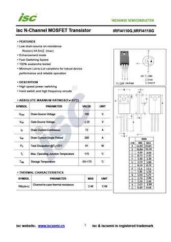
isc N-Channel MOSFET Transistor IRFI4110G,IIRFI4110G FEATURES Low drain-source on-resistance RDS(on) 4.5m (max) Enhancement mode Fast Switching Speed 100% avalanche tested Minimum Lot-to-Lot variations for robust device performance and reliable operation DESCRITION High speed power switching Hard switch and high frequency circuits ABSOLUTE MAXIMUM RATINGS(
irfsl4115.pdf
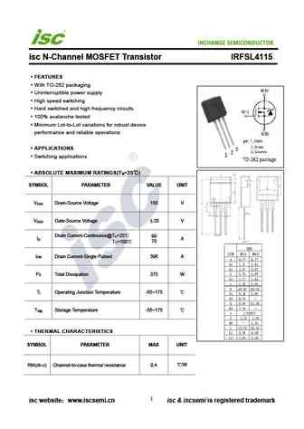
INCHANGE Semiconductor isc N-Channel MOSFET Transistor IRFSL4115 FEATURES With TO-262 packaging Uninterruptible power supply High speed switching Hard switched and high frequency circuits 100% avalanche tested Minimum Lot-to-Lot variations for robust device performance and reliable operationz APPLICATIONS Switching applications ABSOLUTE MAXIMUM RATINGS(T =25 )
irfb4110.pdf
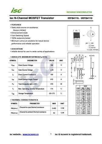
isc N-Channel MOSFET Transistor IRFB4110 IIRFB4110 FEATURES Static drain-source on-resistance RDS(on) 4.5m Enhancement mode Fast Switching Speed 100% avalanche tested Minimum Lot-to-Lot variations for robust device performance and reliable operation DESCRITION reliable device for use in a wide variety of applications ABSOLUTE MAXIMUM RATINGS(T =25 ) a S
2sk4118ls.pdf

isc N-Channel MOSFET Transistor 2SK4118LS FEATURES Drain Current I = 18A@ T =25 D C Drain Source Voltage V = 400V(Min) DSS Static Drain-Source On-Resistance R = 0.34 (Max) @ V = 10V DS(on) GS 100% avalanche tested Minimum Lot-to-Lot variations for robust device performance and reliable operation DESCRIPTION motor drive, DC-DC converter, power switch and sole
2n4114.pdf

isc Silicon NPN Power Transistor 2N4114 DESCRIPTION Excellent Safe Operating Area Low Collector-Emitter Saturation Voltage 100% avalanche tested Minimum Lot-to-Lot variations for robust device performance and reliable operation. APPLICATIONS Designed for general-purpose switching and amplifier applications ABSOLUTE MAXIMUM RATINGS(T =25 ) a SYMBOL PARAMETER VALUE UNIT V
2sc5411.pdf
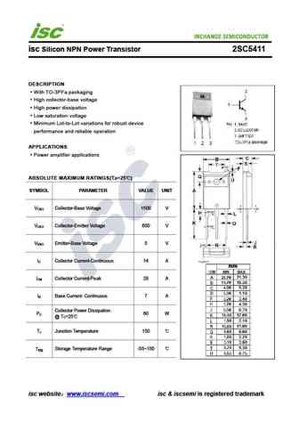
isc Silicon NPN Power Transistor 2SC5411 DESCRIPTION With TO-3PFa packaging High collector-base voltage High power dissipation Low saturation voltage Minimum Lot-to-Lot variations for robust device performance and reliable operation APPLICATIONS Power amplifier applications ABSOLUTE MAXIMUM RATINGS(Ta=25 ) SYMBOL PARAMETER VALUE UNIT V Collector-Base Voltage 1500 V CB
irfu3411.pdf
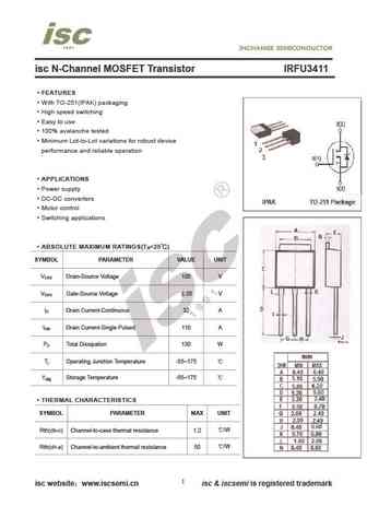
isc N-Channel MOSFET Transistor IRFU3411 FEATURES With TO-251(IPAK) packaging High speed switching Easy to use 100% avalanche tested Minimum Lot-to-Lot variations for robust device performance and reliable operation APPLICATIONS Power supply DC-DC converters Motor control Switching applications ABSOLUTE MAXIMUM RATINGS(T =25 ) a SYMBOL PARAMETER VALUE UN
irfp4110.pdf
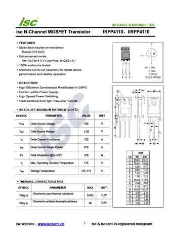
INCHANGE Semiconductor isc N-Channel MOSFET Transistor IRFP4110 IIRFP4110 FEATURES Static drain-source on-resistance RDS(on) 4.5m Enhancement mode Vth =2.0 to 4.0 V (VDS=VGS, ID=250 A) 100% avalanche tested Minimum Lot-to-Lot variations for robust device performance and reliable operation DESCRITION High Efficiency Synchronous Rectification in SMPS Uninterr
2sk4119ls.pdf

isc N-Channel MOSFET Transistor 2SK4119LS FEATURES Drain Current I = 21A@ T =25 D C Drain Source Voltage V = 400V(Min) DSS Static Drain-Source On-Resistance R = 0.26 (Max) @ V = 10V DS(on) GS 100% avalanche tested Minimum Lot-to-Lot variations for robust device performance and reliable operation DESCRIPTION motor drive, DC-DC converter, power switch and sole
2n4113.pdf

isc Silicon NPN Power Transistor 2N4113 DESCRIPTION Excellent Safe Operating Area Low Collector-Emitter Saturation Voltage 100% avalanche tested Minimum Lot-to-Lot variations for robust device performance and reliable operation. APPLICATIONS Designed for general-purpose switching and amplifier applications ABSOLUTE MAXIMUM RATINGS(T =25 ) a SYMBOL PARAMETER VALUE UNIT V
2sd1411.pdf
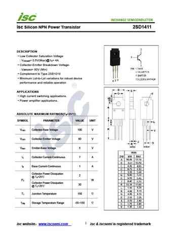
isc Silicon NPN Power Transistor 2SD1411 DESCRIPTION Low Collector Saturation Voltage V = 0.5V(Max)@ I = 4A CE(sat) C Collector-Emitter Breakdown Voltage- V = 80V (Min) (BR)CEO Complement to Type 2SB1018 Minimum Lot-to-Lot variations for robust device performance and reliable operation APPLICATIONS High current switching applications. Power amplifier applications.
mj411.pdf
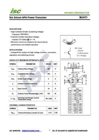
isc Silicon NPN Power Transistor MJ411 DESCRIPTION High Collector-Emitter Sustaining Voltage- V = 300V(Min.) CEO(SUS) Collector-Emitter Saturation Voltage- V )= 0.8 V(Max)@ I = 1A CE(sat C Minimum Lot-to-Lot variations for robust device performance and reliable operation APPLICATIONS Designed for medium to high voltage inverters, converters, regulators and switching circ
2sk1411.pdf
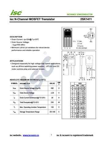
isc N-Channel MOSFET Transistor 2SK1411 DESCRIPTION Drain Current I =20A@ T =25 D C Drain Source Voltage- V =500 (Min) DSS Minimum Lot-to-Lot variations for robust device performance and reliable operation APPLICATIONS Designed especially for high voltage,high speed applications, such as off-line switching power supplies , UPS,AC and DC motor controls,relay and solen
2sk4116ls.pdf

isc N-Channel MOSFET Transistor 2SK4116LS FEATURES Drain Current I = 12A@ T =25 D C Drain Source Voltage V = 400V(Min) DSS Static Drain-Source On-Resistance R = 0.54 (Max) @ V = 10V DS(on) GS 100% avalanche tested Minimum Lot-to-Lot variations for robust device performance and reliable operation DESCRIPTION motor drive, DC-DC converter, power switch and sole
2sc4110-f2.pdf
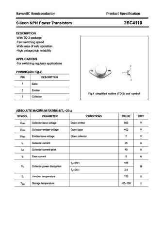
SavantIC Semiconductor Product Specification Silicon NPN Power Transistors 2SC4110 DESCRIPTION With TO-3 package Fast switching speed Wide area of safe operation High voltage,high reliability APPLICATIONS For switching regulator applications PINNING(see Fig.2) PIN DESCRIPTION 1 Base 2 Emitter Fig.1 simplified outline (TO-3) and symbol 3 Collector ABSOLUTE
2n4111.pdf
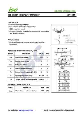
isc Silicon NPN Power Transistor 2N4111 DESCRIPTION Excellent Safe Operating Area Low Collector-Emitter Saturation Voltage 100% avalanche tested Minimum Lot-to-Lot variations for robust device performance and reliable operation. APPLICATIONS Designed for general-purpose switching and amplifier applications ABSOLUTE MAXIMUM RATINGS(T =25 ) a SYMBOL PARAMETER VALUE UNIT V
2sk4117ls.pdf
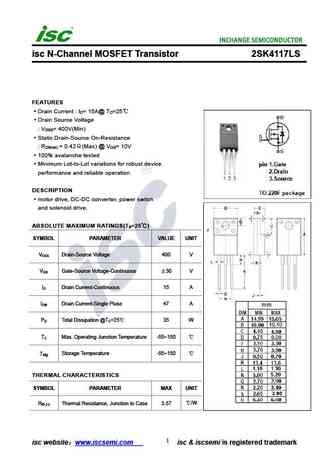
isc N-Channel MOSFET Transistor 2SK4117LS FEATURES Drain Current I = 15A@ T =25 D C Drain Source Voltage V = 400V(Min) DSS Static Drain-Source On-Resistance R = 0.42 (Max) @ V = 10V DS(on) GS 100% avalanche tested Minimum Lot-to-Lot variations for robust device performance and reliable operation DESCRIPTION motor drive, DC-DC converter, power switch and sole
2sc4116.pdf
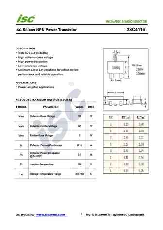
isc Silicon NPN Power Transistor 2SC4116 DESCRIPTION With SOT-323 packaging High collector-base voltage High power dissipation Low saturation voltage Minimum Lot-to-Lot variations for robust device performance and reliable operation APPLICATIONS Power amplifier applications ABSOLUTE MAXIMUM RATINGS(Ta=25 ) SYMBOL PARAMETER VALUE UNIT V Collector-Base Voltage 60 V CBO
aob411l.pdf
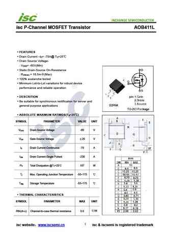
isc P-Channel MOSFET Transistor AOB411L FEATURES Drain Current I = -78A@ T =25 D C Drain Source Voltage- V = -60V(Min) DSS Static Drain-Source On-Resistance R = 16.5m (Max) DS(on) 100% avalanche tested Minimum Lot-to-Lot variations for robust device performance and reliable operation DESCRITION Be suitable for synchronous rectification for server and ge
2sb1411.pdf
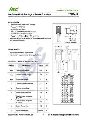
isc Silicon PNP Darlington Power Transistor 2SB1411 DESCRIPTION Collector-Emitter Breakdown Voltage- V = -100V(Min) (BR)CEO High DC Current Gain- h = 1500(Min)@ (V = -3V, I = -1A) FE CE C Low Collector Saturation Voltage- V = -1.5V(Max)@ (I = -1A, I = -2mA) CE(sat) C B Minimum Lot-to-Lot variations for robust device performance and reliable operation APPLICATIONS H
irfr3411.pdf
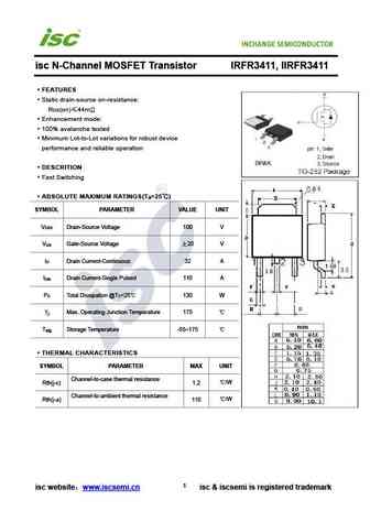
isc N-Channel MOSFET Transistor IRFR3411, IIRFR3411 FEATURES Static drain-source on-resistance RDS(on) 44m Enhancement mode 100% avalanche tested Minimum Lot-to-Lot variations for robust device performance and reliable operation DESCRITION Fast Switching ABSOLUTE MAXIMUM RATINGS(T =25 ) a SYMBOL PARAMETER VALUE UNIT V Drain-Source Voltage 100 V DSS V Gate
2sc4111.pdf
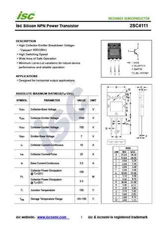
isc Silicon NPN Power Transistor 2SC4111 DESCRIPTION High Collector-Emitter Breakdown Voltage- V = 800V(Min) (BR)CEO High Switching Speed Wide Area of Safe Operation Minimum Lot-to-Lot variations for robust device performance and reliable operation APPLICATIONS Designed for horizontal output applications. ABSOLUTE MAXIMUM RATINGS(T =25 ) a SYMBOL PARAMETER VALUE UNIT
irfb4110g.pdf
isc N-Channel MOSFET Transistor IRFB4110G IIRFB4110G FEATURES Static drain-source on-resistance RDS(on) 4.5m Enhancement mode Fast Switching Speed 100% avalanche tested Minimum Lot-to-Lot variations for robust device performance and reliable operation DESCRITION reliable device for use in a wide variety of applications ABSOLUTE MAXIMUM RATINGS(T =25 ) a
2sc4110.pdf
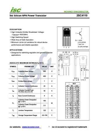
isc Silicon NPN Power Transistor 2SC4110 DESCRIPTION High Collector-Emitter Breakdown Voltage- V = 400V(Min) (BR)CEO High Switching Speed Wide Area of Safe Operation Minimum Lot-to-Lot variations for robust device performance and reliable operation APPLICATIONS Designed for switching regulator and general purpose applications. ABSOLUTE MAXIMUM RATINGS(T =25 ) a SYMBO
irfb4115.pdf
isc N-Channel MOSFET Transistor IRFB4115 IIRFB4115 FEATURES Static drain-source on-resistance RDS(on) 11m Enhancement mode Fast Switching Speed 100% avalanche tested Minimum Lot-to-Lot variations for robust device performance and reliable operation DESCRITION High Efficiency Synchronous Rectification in SMPS Uninterruptible Power Supply ABSOLUTE MAXIMUM
irfs4115pbf.pdf
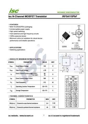
INCHANGE Semiconductor isc N-Channel MOSFET Transistor IRFS4115PbF FEATURES With TO-263(D2PAK) packaging Uninterruptible power supply High speed switching Hard switched and high frequency circuits 100% avalanche tested Minimum Lot-to-Lot variations for robust device performance and reliable operationz APPLICATIONS Switching applications ABSOLUTE MAXIMUM RATINGS(T
Другие транзисторы... 41025 , 41026 , 41027 , 41028 , 41038 , 41039 , 41042 , 41044 , 2SC2625 , 413 , 41500 , 41501 , 41502 , 41503 , 41504 , 41505 , 41506 .


Список транзисторов
Обновления
BJT: GA1A4M | SBT42 | 2SA200-Y | 2SA200-O | 2SD882-Q | 2SD882-P | 2SD882-E | 2SC945-L | 2SC945-H | 2SC4226-R23 | 2SC3357-F | 2SC3357-E | 2SC3356-R26 | 2SC3356-R24 | 2SC3356-R23 | 2SB772-Q | 2SB772-P | 2SB772-E | 2SA1015-L | 2SA1015-H | HSS8550
Popular searches
mp40 transistor | fgpf4636 datasheet | 2sc1945 | c2383 | 2sb681 | bc639 equivalent | bd138 transistor equivalent | c1096 transistor