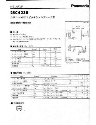
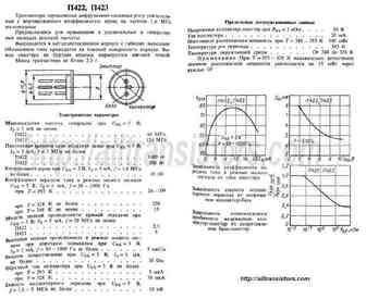
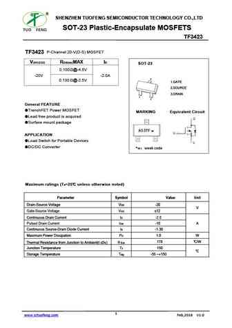
423 datasheet, аналоги, основные параметры
Наименование производителя: 423
Тип материала: Si
Полярность: NPN
Предельные значения
Максимальная рассеиваемая мощность (Pc): 125 W
Макcимально допустимое напряжение коллектор-база (Ucb): 400 V
Макcимально допустимое напряжение коллектор-эмиттер (Uce): 325 V
Макcимально допустимое напряжение эмиттер-база (Ueb): 5 V
Макcимальный постоянный ток коллектора (Ic): 7 A
Предельная температура PN-перехода (Tj): 150 °C
Электрические характеристики
Граничная частота коэффициента передачи тока (ft): 4 MHz
Статический коэффициент передачи тока (hFE): 40
Корпус транзистора: TO3
Аналоги (замена) для 423
- подборⓘ биполярного транзистора по параметрам
423 даташит
aon7423.pdf
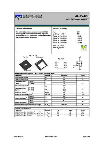
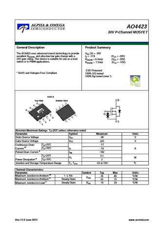
AON7423 20V P-Channel MOSFET General Description Product Summary VDS -20V The AON7423 combines advanced trench MOSFET technology with a low resistance package to provide ID (at VGS=-4.5V) -50A extremely low RDS(ON). This device is ideal for load switch RDS(ON) (at VGS=-4.5V)
me7423s-g.pdf
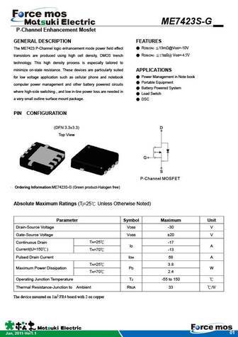
ME7423S-G P-Channel Enhancement Mosfet GENERAL DESCRIPTION FEATURES RDS(ON) 13m @VGS=-10V The ME7423 P-Channel logic enhancement mode power field effect RDS(ON) 17m @ VGS=-4.5V transistors are produced using high cell density, DMOS trench technology. This high density process is especially tailored to minimize on-state resistance. These devices are particular
ntmfs5c423nlt1g.pdf
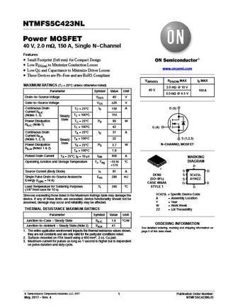
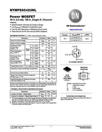
NTMFS5C423NL Power MOSFET 40 V, 2.0 mW, 150 A, Single N-Channel Features Small Footprint (5x6 mm) for Compact Design Low RDS(on) to Minimize Conduction Losses www.onsemi.com Low QG and Capacitance to Minimize Driver Losses These Devices are Pb-Free and are RoHS Compliant V(BR)DSS RDS(ON) MAX ID MAX MAXIMUM RATINGS (TJ = 25 C unless otherwise noted) 2.0 mW @ 10 V 40
bf421 bf423.pdf
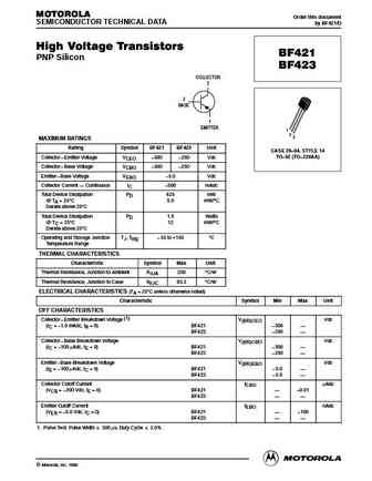
MOTOROLA Order this document SEMICONDUCTOR TECHNICAL DATA by BF421/D High Voltage Transistors BF421 PNP Silicon BF423 COLLECTOR 2 3 BASE 1 EMITTER 1 2 3 MAXIMUM RATINGS Rating Symbol BF421 BF423 Unit CASE 29 04, STYLE 14 TO 92 (TO 226AA) Collector Emitter Voltage VCEO 300 250 Vdc Collector Base Voltage VCBO 300 250 Vdc Emitter Base Voltage VEBO
irfhm4231.pdf
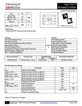
FastIRFET IRFHM4231TRPbF HEXFET Power MOSFET VDSS 25 V RDS(on) max 3.4 (@ VGS = 10V) m (@ VGS = 4.5V) 4.6 Qg (typical) 9.7 nC ID 40 A (@TC (Bottom) = 25 C) PQFN 3.3 x 3.3 mm Applications Control MOSFET for synchronous buck converter Features Benefits Low Charge (typical 9.7nC) Low Switching Losses Low RDSon (
irfh4234.pdf
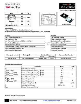
FastIRFET IRFH4234PbF HEXFET Power MOSFET VDSS 25 V RDS(on) max 4.6 (@ VGS = 10V) m (@ VGS = 4.5V) 7.3 Qg (typical) 8.2 nC ID 60 A PQFN 5X6 mm (@TC (Bottom) = 25 C) Applications Control MOSFET for Sync Buck Converters Secondary Synchronous Rectifier MOSFET for isolated DC-DC converters Features Benefits Low Charge (typical 8.2 nC) Lo
irfp4232pbf.pdf
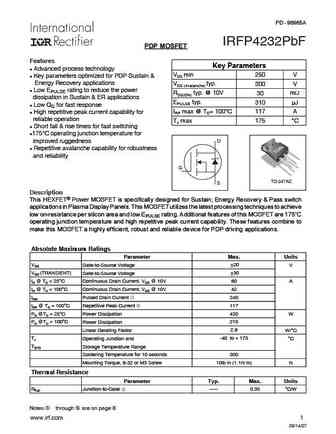
PD - 96965A IRFP4232PbF PDP MOSFET Features Key Parameters l Advanced process technology VDS min 250 V l Key parameters optimized for PDP Sustain & Energy Recovery applications VDS (Avalanche) typ. 300 V l Low EPULSE rating to reduce the power m RDS(ON) typ. @ 10V 30 dissipation in Sustain & ER applications EPULSE typ. 310 J l Low QG for fast response IRP max @ TC= 100 C l
irfhm4234.pdf

FastIRFET IRFHM4234TRPbF HEXFET Power MOSFET Top View VDSS 25 V RDS(on) max 4.4 D 5 4 G (@ VGS = 10V) m D 6 3 S (@ VGS = 4.5V) 7.1 D 7 2 S Qg (typical) 8.2 nC D 8 1 S ID 60 A (@TC (Bottom) = 25 C) PQFN 3.3 x 3.3 mm Applications Control MOSFET for synchronous buck converter Features Benefits Low Charge (typical 8.2 nC) Low Switching
irfb4233pbf.pdf
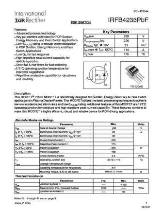
PD - 97004A IRFB4233PbF PDP SWITCH Features Key Parameters l Advanced process technology VDS min 230 V l Key parameters optimized for PDP Sustain, Energy Recovery and Pass Switch Applications VDS (Avalanche) typ. 276 V l Low EPULSE rating to reduce power dissipation m RDS(ON) typ. @ 10V 31 in PDP Sustain, Energy Recovery and Pass IRP max @ TC= 100 C 114 A Switch Applications
bf421 bf423.pdf

DISCRETE SEMICONDUCTORS DATA SHEET book, halfpage M3D186 BF421; BF423 PNP high-voltage transistors 1996 Dec 09 Product specification Supersedes data of September 1994 File under Discrete Semiconductors, SC04 Philips Semiconductors Product specification PNP high-voltage transistors BF421; BF423 FEATURES PINNING Low feedback capacitance. PIN DESCRIPTION 1 base APPLICATIONS 2
bf421 bf423 2.pdf
DISCRETE SEMICONDUCTORS DATA SHEET book, halfpage M3D186 BF421; BF423 PNP high voltage transistors Product specification 2004 Nov 10 Supersedes data of 1996 Dec 09 Philips Semiconductors Product specification PNP high voltage transistors BF421; BF423 FEATURES PINNING Low feedback capacitance. PIN DESCRIPTION 1 base APPLICATIONS 2 collector Class-B video output stages in
bf421 bf423 1.pdf
DISCRETE SEMICONDUCTORS DATA SHEET book, halfpage M3D186 BF421; BF423 PNP high-voltage transistors 1996 Dec 09 Product specification Supersedes data of September 1994 File under Discrete Semiconductors, SC04 Philips Semiconductors Product specification PNP high-voltage transistors BF421; BF423 FEATURES PINNING Low feedback capacitance. PIN DESCRIPTION 1 base APPLICATIONS 2
bf421l bf423l.pdf
DISCRETE SEMICONDUCTORS DATA SHEET book, halfpage M3D186 BF421L; BF423L PNP high-voltage transistors 1999 Apr 21 Product specification Supersedes data of 1997 Apr 18 Philips Semiconductors Product specification PNP high-voltage transistors BF421L; BF423L FEATURES PINNING Low current (max. 50 mA) PIN DESCRIPTION High voltage (max. 300 V) 1 base Available with a highe
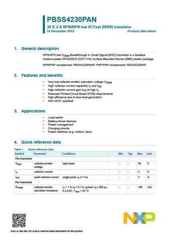
pbss4230t.pdf
DISCRETE SEMICONDUCTORS DATA SHEET M3D088 PBSS4230T 30 V, 2 A NPN low VCEsat (BISS) transistor Product data sheet 2003 Sep 29 NXP Semiconductors Product data sheet 30 V, 2 A PBSS4230T NPN low VCEsat (BISS) transistor FEATURES QUICK REFERENCE DATA Low collector-emitter saturation voltage VCEsat SYMBOL PARAMETER MAX. UNIT High collector current capability IC and ICM VC
sd1423.pdf
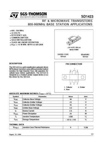
SD1423 RF & MICROWAVE TRANSISTORS 800-960MHz BASE STATION APPLICATIONS .800 - 960 MHz .24 VOLTS .EFFICIENCY 50% .COMMON EMITTER .GOLD METALLIZATION .CLASS AB LINEAR OPERATION .P 15 W MIN. WITH 8.0 dB GAIN OUT = .230 6LFL (M118) epoxy sealed ORDE R CODE BRANDING SD1423 SD1423 DESCRIPTION PIN CONNECTION The SD1423 is a gold metallization epitaxial silicon NPN planar transistor
2sc3423.pdf
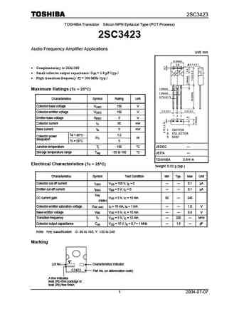
2SC3423 TOSHIBA Transistor Silicon NPN Epitaxial Type (PCT Process) 2SC3423 Audio Frequency Amplifier Applications Unit mm Complementary to 2SA1360 Small collector output capacitance Cob = 1.8 pF (typ.) High transition frequency fT = 200 MHz (typ.) Maximum Ratings (Tc = 25 C) Characteristics Symbol Rating Unit Collector-base voltage VCBO 150 V Collector-emitt
sft1423.pdf
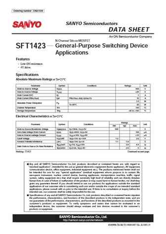
SFT1423 Ordering number ENA1509 SANYO Semiconductors DATA SHEET N-Channel Silicon MOSFET General-Purpose Switching Device SFT1423 Applications Features Low ON-resistance. 4V drive. Specifications at Ta=25 C Absolute Maximum Ratings Parameter Symbol Conditions Ratings Unit Drain-to-Source Voltage VDSS 500 V Gate-to-Source Voltage VGSS 20 V Drain Current (DC) ID 2 A
2sk1423.pdf
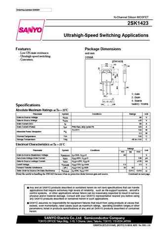
Ordering number EN3561 N-Channel Silicon MOSFET 2SK1423 Ultrahigh-Speed Switching Applications Features Package Dimensions Low ON-state resistance. unit mm Ultrahigh-speed switching. 2056A Converters. [2SK1423] 15.6 3.2 4.8 14.0 2.0 1.6 2.0 0.6 1.0 1 2 3 1 Gate 0.6 2 Drain 3 Source 5.45 5.45 SANYO TO3PB Specifications Absolute Maximum Ratings at Ta
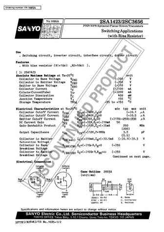
2sc4423.pdf
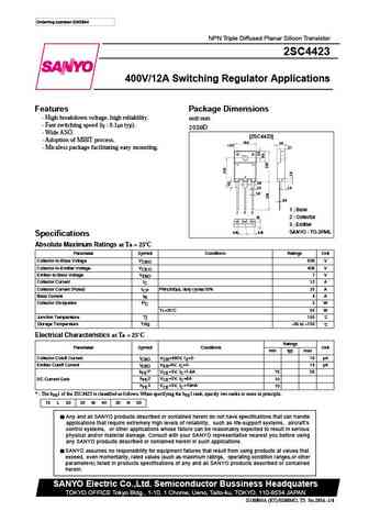
Ordering number EN2854 NPN Triple Diffused Planar Silicon Transistor 2SC4423 400V/12A Switching Regulator Applications Features Package Dimensions High breakdown voltage, high reliability. unit mm Fast switching speed (tf 0.1 s typ). 2039D Wide ASO. [2SC4423] Adoption of MBIT process. 16.0 5.6 3.4 Micaless package facilitating easy mounting. 3.1 2.8 2.0
hufa76423p3 hufa76423s3s hufa76423s3st.pdf
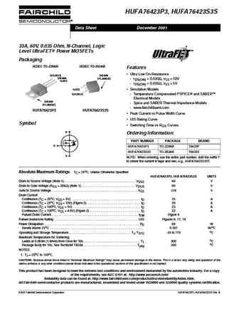
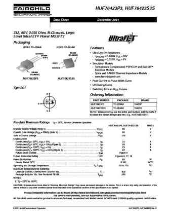
HUFA76423P3, HUFA76423S3S Data Sheet December 2001 33A, 60V, 0.035 Ohm, N-Channel, Logic Level UltraFET Power MOSFETs Packaging JEDEC TO-220AB JEDEC TO-263AB Features Ultra Low On-Resistance SOURCE DRAIN DRAIN (FLANGE) - rDS(ON) = 0.030 , VGS = 10V GATE - rDS(ON) = 0.035 , VGS = 5V GATE Simulation Models SOURCE - Temperature Compensated PSPICE and SABER Ele
huf76423d3s.pdf
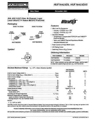
HUF76423D3, HUF76423D3S Data Sheet December 2001 20A, 60V, 0.037 Ohm, N-Channel, Logic Level UltraFET Power MOSFETFairchild Packaging Features JEDEC TO-251AA JEDEC TO-252AA Ultra Low On-Resistance - rDS(ON) = 0.032 , VGS = 10V DRAIN DRAIN - rDS(ON) = 0.037 , VGS = 5V SOURCE (FLANGE) (FLANGE) DRAIN GATE Simulation Models - Temperature Compensated PSPICE and SABER
huf76423p3.pdf
HUF76423P3, HUF76423S3S Data Sheet December 2001 33A, 60V, 0.035 Ohm, N-Channel, Logic Level UltraFET Power MOSFET Packaging JEDEC TO-220AB JEDEC TO-263AB Features DRAIN Ultra Low On-Resistance SOURCE (FLANGE) DRAIN - rDS(ON) = 0.030 , VGS = 10V GATE - rDS(ON) = 0.035 , VGS = 5V GATE Simulation Models - Temperature Compensated PSPICE and SABER SOURCE Elec
hufa76423d3s hufa76423d3st.pdf

HUFA76423D3, HUFA76423D3S Data Sheet December 2001 20A, 60V, 0.037 Ohm, N-Channel, Logic Level UltraFET Power MOSFETs Packaging Features JEDEC TO-251AA JEDEC TO-252AA Ultra Low On-Resistance - rDS(ON) = 0.032 , VGS = 10V DRAIN DRAIN - rDS(ON) = 0.037 , VGS = 5V SOURCE (FLANGE) (FLANGE) DRAIN GATE Simulation Models - Temperature Compensated PSPICE and SABER
pbss4230pan.pdf
PBSS4230PAN 30 V, 2 A NPN/NPN low VCEsat (BISS) transistor 14 December 2012 Product data sheet 1. General description NPN/NPN low VCEsat Breakthrough In Small Signal (BISS) transistor in a leadless medium power DFN2020-6 (SOT1118) Surface-Mounted Device (SMD) plastic package. NPN/PNP complement PBSS4230PANP. PNP/PNP complement PBSS5230PAP. 2. Features and benefits Very low collect
pbss4230panp.pdf
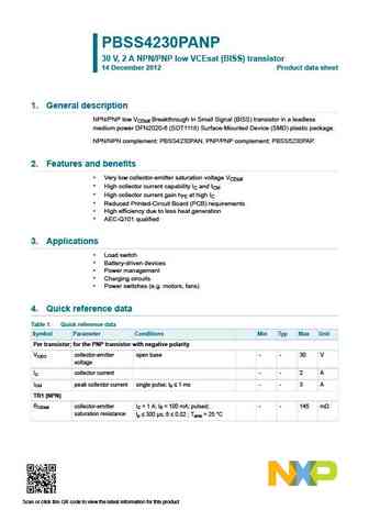
PBSS4230PANP 30 V, 2 A NPN/PNP low VCEsat (BISS) transistor 14 December 2012 Product data sheet 1. General description NPN/PNP low VCEsat Breakthrough In Small Signal (BISS) transistor in a leadless medium power DFN2020-6 (SOT1118) Surface-Mounted Device (SMD) plastic package. NPN/NPN complement PBSS4230PAN. PNP/PNP complement PBSS5230PAP. 2. Features and benefits Very low collect
pbss4230qa.pdf
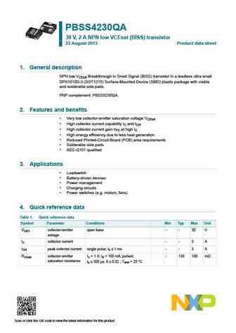
PBSS4230QA 30 V, 2 A NPN low VCEsat (BISS) transistor 23 August 2013 Product data sheet 1. General description NPN low VCEsat Breakthrough In Small Signal (BISS) transistor in a leadless ultra small DFN1010D-3 (SOT1215) Surface-Mounted Device (SMD) plastic package with visible and solderable side pads. PNP complement PBSS5230QA. 2. Features and benefits Very low collector-emitter
pbss4230t.pdf

Important notice Dear Customer, On 7 February 2017 the former NXP Standard Product business became a new company with the tradename Nexperia. Nexperia is an industry leading supplier of Discrete, Logic and PowerMOS semiconductors with its focus on the automotive, industrial, computing, consumer and wearable application markets In data sheets and application notes which still contain
bf421 bf423.pdf
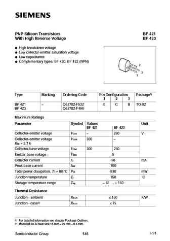
PNP Silicon Transistors BF 421 With High Reverse Voltage BF 423 High breakdown voltage Low collector-emitter saturation voltage Low capacitance Complementary types BF 420, BF 422 (NPN) 2 3 1 Type Marking Ordering Code Pin Configuration Package1) 1 2 3 BF 421 Q62702-F532 E C B TO-92 BF 423 Q62702-F496 Maximum Ratings Parameter Symbol Values Unit BF 421 BF 423 Collector-e
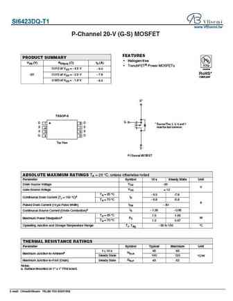
si6423dq.pdf
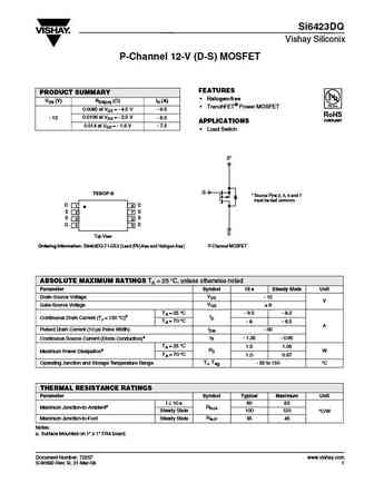
Si6423DQ Vishay Siliconix P-Channel 12-V (D-S) MOSFET FEATURES PRODUCT SUMMARY Halogen-free VDS (V) RDS(on) ( )ID (A) TrenchFET Power MOSFET 0.0085 at VGS = - 4.5 V - 9.5 RoHS 0.0106 at VGS = - 2.5 V - 12 - 8.5 COMPLIANT APPLICATIONS 0.014 at VGS = - 1.8 V - 7.5 Load Switch S* G TSSOP-8 * Source Pins 2, 3, 6 and 7 must be tied common. D D 1 8 S S
u421 u423.pdf
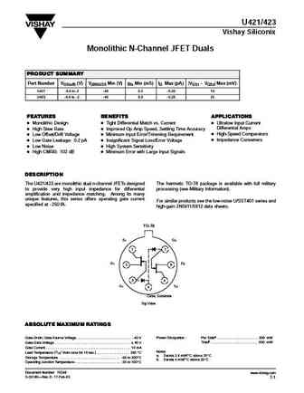
U421/423 Vishay Siliconix Monolithic N-Channel JFET Duals PRODUCT SUMMARY Part Number VGS(off) (V) V(BR)GSS Min (V) gfs Min (mS) IG Max (pA) jVGS1 - VGS2j Max (mV) U421 -0.4 to-2 -40 0.3 -0.25 10 U423 -0.4 to -2 -40 0.3 -0.25 25 FEATURES BENEFITS APPLICATIONS D Monolithic Design D Tight Differential Match vs. Current D Ultralow Input Current Differential Amps D High Slew Rate D Improv
sqs423en.pdf
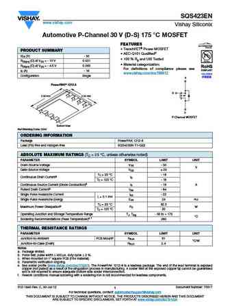
SQS423EN www.vishay.com Vishay Siliconix Automotive P-Channel 30 V (D-S) 175 C MOSFET FEATURES TrenchFET Power MOSFET PRODUCT SUMMARY AEC-Q101 Qualifiedd VDS (V) - 30 100 % Rg and UIS Tested RDS(on) ( ) at VGS = - 10 V 0.021 Material categorization RDS(on) ( ) at VGS = - 4.5 V 0.060 For definitions of compliance please see ID (A) - 16 www.vishay.com/d
si4423dy.pdf
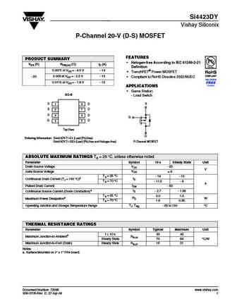
Si4423DY Vishay Siliconix P-Channel 20-V (D-S) MOSFET FEATURES PRODUCT SUMMARY Halogen-free According to IEC 61249-2-21 VDS (V) RDS(on) ( )ID (A) Definition 0.0075 at VGS = - 4.5 V - 14 TrenchFET Power MOSFET 0.009 at VGS = - 2.5 V - 13 - 20 Compliant to RoHS Directive 2002/95/EC 0.0115 at VGS = - 1.8 V - 12 APPLICATIONS Game Station SO-8 - Load Switc
si7423dn.pdf

Si7423DN Vishay Siliconix P-Channel 30-V (D-S) MOSFET FEATURES PRODUCT SUMMARY Halogen-free According to IEC 61249-2-21 VDS (V) RDS(on) ( )ID (A) Available 0.018 at VGS = - 10 V - 11.7 TrenchFET Power MOSFET - 30 0.030 at VGS = - 4.5 V - 9.0 New PowerPAK Package - Low Thermal Resistance, RthJC - Low 1.07 mm Profile APPLICATIONS PowerPAK 1212-8 Ba
si4230dy.pdf
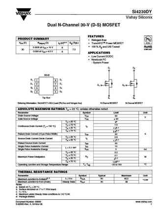
Si4230DY Vishay Siliconix Dual N-Channel 30-V (D-S) MOSFET FEATURES PRODUCT SUMMARY Halogen-free VDS (V) RDS(on) ( ) ID (A)a, e Qg (Typ.) TrenchFET Power MOSFET 100 % Rg and UIS Tested 0.0205 at VGS = 10 V 8 30 7.3 0.026 at VGS = 4.5 V 8 APPLICATIONS Low Current DC/DC Notebook PC - System Power D1 D2 SO-8 S1 1 D1 8 G1 2 D1 7 G1 G2 S2 3 D
2n4237 2n4238 2n4239.pdf
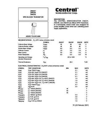
TM 2N4237 Central 2N4238 Semiconductor Corp. 2N4239 NPN SILICON TRANSISTOR DESCRIPTION The CENTRAL SEMICONDUCTOR 2N4237, 2N4238, and 2N4239 are Silicon NPN Transistors, in a hermetically sealed metal case designed for power amplifier, power driver and switching power supply applications. JEDEC TO-39 CASE MAXIMUM RATINGS (TC=25 C unless otherwise noted) SYMBOL 2N4237 2N4238 2N
om6423sp6.pdf
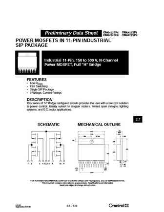
OM6423SP6 OM6425SP6 Preliminary Data Sheet OM6424SP6 OM6426SP6 POWER MOSFETS IN 11-PIN INDUSTRIAL SIP PACKAGE Industrial 11-Pin, 150 to 500 V, N-Channel Power MOSFET, Full H Bridge FEATURES Low RDS(on) Fast Switching Single SIP Package 3 Voltage, Current Ratings DESCRIPTION This series of H Bridge configured circuits provides the user with a low cost sol
bf421 bf423.pdf
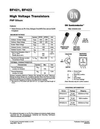
BF421, BF423 High Voltage Transistors PNP Silicon Features These Devices are Pb-Free, Halogen Free/BFR Free and are RoHS http //onsemi.com Compliant MAXIMUM RATINGS Rating Symbol BF421 BF423 Unit TO-92 Collector-Emitter Voltage VCEO -300 -250 Vdc CASE 29 STYLE 14 Collector-Base Voltage VCBO -300 -250 Vdc 1 1 2 2 Emitter-Base Voltage VEBO -5.0 Vdc 3 3 STRAIGHT LEAD BENT
huf76423p3.pdf

Is Now Part of To learn more about ON Semiconductor, please visit our website at www.onsemi.com Please note As part of the Fairchild Semiconductor integration, some of the Fairchild orderable part numbers will need to change in order to meet ON Semiconductor s system requirements. Since the ON Semiconductor product management systems do not have the ability to manage part nomenclatur
ntmfs5c423nl.pdf
NTMFS5C423NL Power MOSFET 40 V, 2.0 mW, 150 A, Single N-Channel Features Small Footprint (5x6 mm) for Compact Design Low RDS(on) to Minimize Conduction Losses Low QG and Capacitance to Minimize Driver Losses www.onsemi.com These Devices are Pb-Free and are RoHS Compliant V(BR)DSS RDS(ON) MAX ID MAX MAXIMUM RATINGS (TJ = 25 C unless otherwise noted) 2.0 mW @ 10 V Par
nvmfs5c423nl.pdf
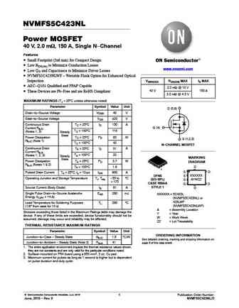
NVMFS5C423NL Power MOSFET 40 V, 2.0 mW, 150 A, Single N-Channel Features Small Footprint (5x6 mm) for Compact Design Low RDS(on) to Minimize Conduction Losses www.onsemi.com Low QG and Capacitance to Minimize Driver Losses NVMFS5C423NLWF - Wettable Flank Option for Enhanced Optical Inspection V(BR)DSS RDS(ON) MAX ID MAX AEC-Q101 Qualified and PPAP Capable 2.0 mW
2sc5423.pdf
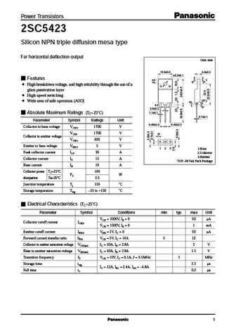
Power Transistors 2SC5423 Silicon NPN triple diffusion mesa type For horizontal deflection output Unit mm 15.5 0.5 3.0 0.3 3.2 0.1 Features 5 5 High breakdown voltage, and high reliability through the use of a glass passivation layer High-speed switching 5 Wide area of safe operation (ASO) 5 4.0 5 2.0 0.2 1.1 0.1 Absolute Maximum Ratings (TC=25 C) 0.
2sd1423 e.pdf
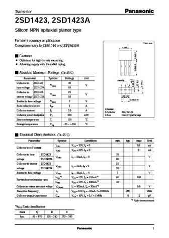
Transistor 2SD1423, 2SD1423A Silicon NPN epitaxial planer type For low-frequency amplification Unit mm Complementary to 2SB1030 and 2SB1030A 4.0 0.2 Features Optimum for high-density mounting. Allowing supply with the radial taping. Absolute Maximum Ratings (Ta=25 C) Parameter Symbol Ratings Unit marking Collector to 2SD1423 30 VCBO V 1 2 3 base voltage 2SD1423A 60 Collector
2sd1423.pdf

Transistor 2SD1423, 2SD1423A Silicon NPN epitaxial planer type For low-frequency amplification Unit mm Complementary to 2SB1030 and 2SB1030A 4.0 0.2 Features Optimum for high-density mounting. Allowing supply with the radial taping. Absolute Maximum Ratings (Ta=25 C) Parameter Symbol Ratings Unit marking Collector to 2SD1423 30 VCBO V 1 2 3 base voltage 2SD1423A 60 Collector
ut4232.pdf
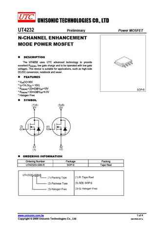
UNISONIC TECHNOLOGIES CO., LTD UT4232 Preliminary Power MOSFET N-CHANNEL ENHANCEMENT MODE POWER MOSFET DESCRIPTION The UT4232 uses UTC advanced technology to provide excellent RDS(ON), low gate charge and to be operated with low gate voltages. This device is suitable for applications, such as high-side DC/DC conversion, notebook and sever. FEATURES * VDS(V)=30V * ID=7A
2sd2423.pdf
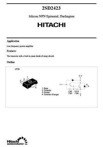
2SD2423 Silicon NPN Epitaxial, Darlington Application Low frequency power amplifier Features The transistor with a built-in zener diode of surge absorb. Outline UPAK 2, 4 1 2 3 1 ID 4 1. Base 2. Collector 2 k 0.5 3. Emitter (Typ) (Typ) 4. Collector (Flange) 3 2SD2423 Absolute Maximum Ratings (Ta = 25 C) Item Symbol Ratings Unit Collector to base voltage VCBO 50
2sk2423.pdf
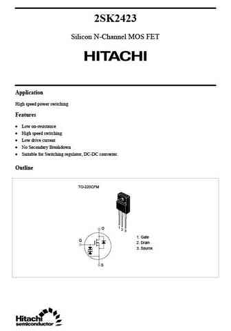
2SK2423 Silicon N-Channel MOS FET Application High speed power switching Features Low on-resistance High speed switching Low drive current No Secondary Breakdown Suitable for Switching regulator, DC-DC converter. Outline TO-220CFM 1 D 2 3 1. Gate G 2. Drain 3. Source S 2SK2423 Absolute Maximum Ratings (Ta = 25 C) Item Symbol Ratings Unit Drain to so
2n4236x.pdf
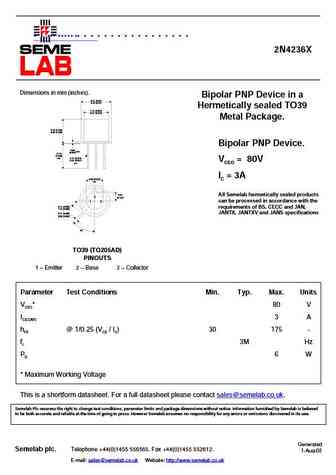
"2N4236X" 2N4236X Dimensions in mm (inches). Bipolar PNP Device in a 8.51 (0.34) 9.40 (0.37) Hermetically sealed TO39 7.75 (0.305) 8.51 (0.335) Metal Package. 6.10 (0.240) 6.60 (0.260) Bipolar PNP Device. 0.89 max. (0.035) 12.70 (0.500) min. 0.41 (0.016) 0.53 (0.021) VCEO = 80V dia. IC = 3A 5.08 (0.200) typ. 2.54 All Semelab hermetically sealed p
sfn423p.pdf
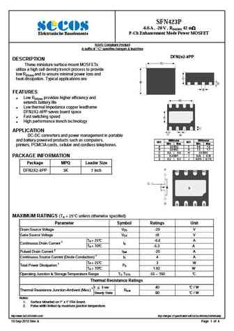
SFN423P -6.6 A , -20 V , RDS(ON) 42 m P-Ch Enhancement Mode Power MOSFET Elektronische Bauelemente RoHS Compliant Product A suffix of -C specifies halogen & lead-free DFN2x2-8PP DESCRIPTION These miniature surface mount MOSFETs utilize a high cell density trench process to provide low RDS(on) and to ensure minimal power loss and heat dissipation. T
stt3423p.pdf
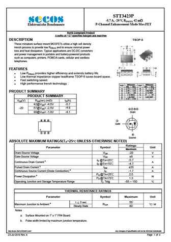
STT3423P -5.7 A, -20 V, RDS(ON) 42 m P-Channel Enhancement Mode Mos.FET Elektronische Bauelemente RoHS Compliant Product A suffix of -C specifies halogen and lead-free DESCRIPTION TSOP-6 These miniature surface mount MOSFETs utilize a high cell density A trench process to provide low RDS(on) and to ensure minimal power E L loss and heat dissipation. Typical applica
tgf4230-scc.pdf
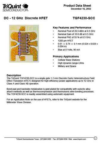
Product Data Sheet December 16, 2002 DC - 12 GHz Discrete HFET TGF4230-SCC Key Features and Performance Nominal Pout of 28.5 dBm at 8.5 GHz Nominal Gain of 10.0 dB at 8.5 GHz Nominal PAE of 55 % at 8.5 GHz 1200 m HFET 0.61 x 0.74 x 0.1 mm (0.024 x 0.029 x 0.004 in) Bias at 8 Volts, 96 mA Primary Applications Cellular Base Stations High dynamic-rang
bc157vi-a bc158vi-a-b bc159a-b bc177v-vi-a-b bc178v-vi-a-b bc179a-b kc307a-b-v kc308a-b-c kc309f-b-c kc636 kc638 kc640 kf423 kf470 kf517.pdf
2n4234 2n4235 2n4236.pdf
Boca Semiconductor corp. bocasemi.com http //www.bocasemi.com http //www.bocasemi.com http //www.bocasemi.com http //www.bocasemi.com
2n4237 2n4238 2n4239.pdf
Boca Semicondcutor Corp. bocasemi.com http //www.bocasemi.com http //www.bocasemi.com http //www.bocasemi.com
2n3583 2n3584 2n3585 2n4240 2n6420 2n6421 2n6422 2n6423.pdf
A Boca Semiconductor Corp. http //www.bocasemi.com A http //www.bocasemi.com A http //www.bocasemi.com A http //www.bocasemi.com
2n6312 2n6313 2n6314 2n4231a 2n4232a 2n4233a.pdf
A Boca Semiconductor Corp. BSC http //www.bocasemi.com A Boca Semiconductor Corp. BSC http //www.bocasemi.com A Boca Semiconductor Corp. BSC http //www.bocasemi.com A Boca Semiconductor Corp. BSC http //www.bocasemi.com
bf421 bf423.pdf
Continental Device India Limited An ISO/TS 16949, ISO 9001 and ISO 14001 Certified Company PNP SILICON PLANAR EPITAXIAL HIGH VOLTAGE BF421 VIDEO TRANSISTORS BF423 TO-92 Plastic Package High Voltage Video Amplifier ABSOLUTE MAXIMUM RATINGS(Ta=25 C unless specified otherwise) DESCRIPTION SYMBOL 423 421 UNITS VCEO Collector Emitter Voltage 250 300 V VCBO Collector Base Voltage 250 300
2n4234 5 6.pdf
Continental Device India Limited An ISO/TS 16949 and ISO 9001 Certified Company PNP SILICON PLANAR TRANSISTORS 2N4234, 2N4235 2N4236 TO-39 Metal Can Package General Purpose Transistor ABSOLUTE MAXIMUM RATINGS DESCRIPTION SYMBOL 2N4234 2N4235 2N4236 UNIT VCEO Collector Emitter Voltage 40 60 80 V VCBO Collector Base Voltage 40 60 80 V VEBO Emitter Base Voltage 7.0 V IB Base Curr
bf421 bf423.pdf
JIANGSU CHANGJING ELECTRONICS TECHNOLOGY CO., LTD TO-92 Plastic-Encapsulate Transistors BF421 TRANSISTOR (PNP) TO-92 BF423 1. EMITTER FEATURES Low Feedback Capacitance. 2.COLLECTOR PNP Transistors in a TO-92 Plastic Package. 3. BASE NPN Complements BF420 and BF422 Class-B Video Output Stages in Colour Television and Professional Monitor Equipment. Equivalent Ci
2sc3423.pdf
JMnic Product Specification Silicon NPN Power Transistors 2SC3423 DESCRIPTION With TO-126 package Complement to type 2SA1360 High transition frequency APPLICATIONS Audio frequency amplifier applications PINNING PIN DESCRIPTION 1 Emitter Collector;connected to 2 mounting base 3 Base Absolute maximum ratings(Ta=25 ) SYMBOL PARAMETER CONDITIONS VALUE UNIT
ktb1423.pdf
SEMICONDUCTOR KTB1423 TECHNICAL DATA EPITAXIAL PLANAR PNP TRANSISTOR SWITCHING APPLICATIONS. HAMMER DRIVER, PULSE MOTOR DRIVER A C APPLICATIONS. DIM MILLIMETERS S _ A 10.0 0.3 + _ + B 15.0 0.3 FEATURES E C _ 2.70 0.3 + D High DC Current Gain hFE=1000(Min.) at VCE=-3V, IC=-3A. 0.76+0.09/-0.05 _ E 3.2 0.2 + High Collector Breakdown Voltage VCEO=-120V (Min.) _ F 3.0
bf423.pdf
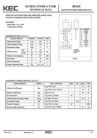
SEMICONDUCTOR BF423 TECHNICAL DATA SILICON PNP TRIPLE DIFFUSED TYPE HIGH VOLTAGE SWITCHING AND AMPLIFIER APPLICATION. COLOR TV CHROMA OUTPUT APPLICATIONS. B C FEATURES High Voltage VCEO>-300V Complementary to BF422. N DIM MILLIMETERS A 4.70 MAX E K B 4.80 MAX G C 3.70 MAX D D 0.45 E 1.00 MAXIMUM RATING (Ta=25 ) F 1.27 G 0.85 CHARACTERISTIC SYMBOL RATING UNIT H 0.45 _
ktc3423.pdf
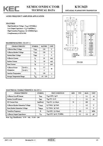
SEMICONDUCTOR KTC3423 TECHNICAL DATA EPITAXIAL PLANAR NPN TRANSISTOR AUDIO FREQUENCY AMPLIFIER APPLICATION. A B D C E FEATURES F High Breakdown Voltage VCEO=150V(Min.). Low Output Capacitance Cob=5.0pF(Max.). G High Transition Frequency fT=120MHz(Typ.). H Complementary to KTA1360. DIM MILLIMETERS J A 8.3 MAX K B 5.8 L C 0.7 _ + D 3.2 0.1 E 3.5 _ + F 11.0 0.
ced3423 ceu3423.pdf
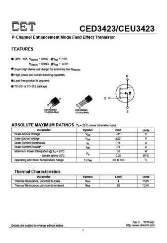
CED3423/CEU3423 P-Channel Enhancement Mode Field Effect Transistor FEATURES -30V, -18A, RDS(ON) = 45m @VGS = -10V. RDS(ON) = 80m @VGS = -4.5V. Super high dense cell design for extremely low RDS(ON). High power and current handing capability. D Lead free product is acquired. TO-251 & TO-252 package. D G G S CEU SERIES CED SERIES S TO-252(D-PAK) TO-251(I-PAK) ABSOLUTE MAX
bf421 bd423.pdf
BF421/BF423(PNP) TO-92 Bipolar Transistors TO-92 1. EMITTER 2. COLLECTOR 3. BASE Features Low feedback capacitance. PNP transistors in a TO-92 plastic package. NPN complements BF420 and BF422 Class-B video output stages in colour television and professional monitor equipment. Dimensions in inches and (millimeters) MAXIMUM RATINGS (TA=25 unless otherwise noted)
hbf423.pdf
Spec. No. HE6403 HI-SINCERITY Issued Date 1993.03.18 Revised Date 2003.06.18 MICROELECTRONICS CORP. Page No. 1/4 HBF423 PNP EPITAXIAL PLANAR TRANSISTOR Description Video B-class Power stages in TV-receivers TO-92 Absolute Maximum Ratings Maximum Temperatures Storage Temperature .............................................................................................
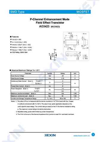
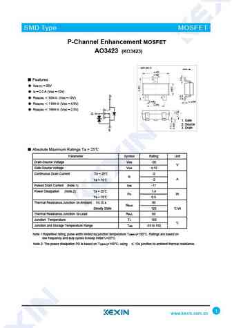
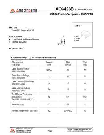
ao3423.pdf
AO3423 20V P-Channel MOSFET General Description Product Summary VDS -20V The AO3423 uses advanced trench technology to provide excellent RDS(ON), low gate charge and operation with gate ID (at VGS=-10V) -2A voltages as low as 2.5V. This device is suitable for use as RDS(ON) (at VGS= -10V)
aoi423.pdf
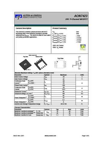
AOD423/AOI423/AOY423 30V P-Channel MOSFET General Description Product Summary VDS -30V The AOD423/AOI423/AOY423 uses advanced trench technology to provide excellent RDS(ON), low gate charge ID (at VGS= -20V) -70A and low gate resistance. With the excellent thermal RDS(ON) (at VGS= -20V)
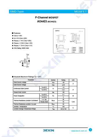
ao4423.pdf
AO4423 30V P-Channel MOSFET General Description Product Summary The AO4423 uses advanced trench technology to provide VDS (V) = -30V excellent RDS(ON), and ultra-low low gate charge with a ID = -17A (VGS = -20V) 25V gate rating. This device is suitable for use as a load RDS(ON)
aon7423.pdf
AON7423 20V P-Channel MOSFET General Description Product Summary VDS -20V The AON7423 combines advanced trench MOSFET technology with a low resistance package to provide ID (at VGS=-4.5V) -50A extremely low RDS(ON). This device is ideal for load switch RDS(ON) (at VGS=-4.5V)
aod423.pdf

AOD423/AOI423/AOY423 30V P-Channel MOSFET General Description Product Summary VDS -30V The AOD423/AOI423/AOY423 uses advanced trench technology to provide excellent RDS(ON), low gate charge ID (at VGS= -20V) -70A and low gate resistance. With the excellent thermal RDS(ON) (at VGS= -20V)
aoy423.pdf

AOD423/AOI423/AOY423 30V P-Channel MOSFET General Description Product Summary VDS -30V The AOD423/AOI423/AOY423 uses advanced trench technology to provide excellent RDS(ON), low gate charge ID (at VGS= -20V) -70A and low gate resistance. With the excellent thermal RDS(ON) (at VGS= -20V)
aod423 aoi423 aoy423.pdf
AOD423/AOI423/AOY423 TM 30V P-Channel AlphaSGT General Description Product Summary VDS -30V The AOD423/AOI423/AOY423 uses advanced trench technology to provide excellent RDS(ON), low gate charge ID (at VGS= -20V) -70A and low gate resistance. With the excellent thermal RDS(ON) (at VGS= -20V)
aoc2423.pdf
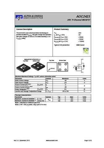
AOC2423 20V P-Channel MOSFET General Description Product Summary VDS -20V The AOC2423 uses advanced trench technology to provide excellent RDS(ON), low gate charge and operation ID (at VGS=-10V) -2A with gate voltages as low as 2.5V while retaining a 12V RDS(ON) (at VGS=-10V)
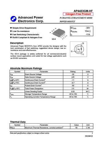
ap4423gm.pdf
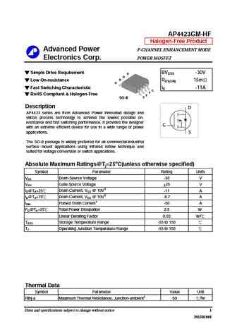
AP4423GM-HF Halogen-Free Product Advanced Power P-CHANNEL ENHANCEMENT MODE Electronics Corp. POWER MOSFET Simple Drive Requirement BVDSS -30V D D D Low On-resistance RDS(ON) 15m D Fast Switching Characteristic ID -11A G S RoHS Compliant & Halogen-Free S S SO-8 Description D AP4423 series are from
ap4230gm-hf.pdf
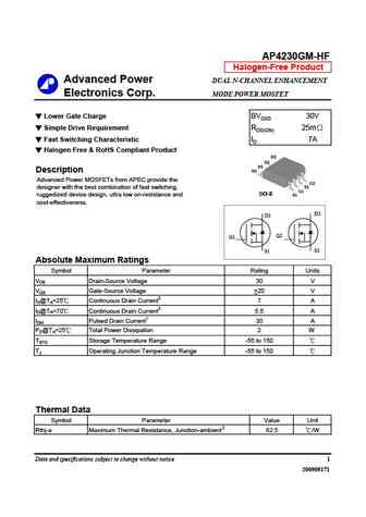
AP4230GM-HF Halogen-Free Product Advanced Power DUAL N-CHANNEL ENHANCEMENT Electronics Corp. MODE POWER MOSFET Lower Gate Charge BVDSS 30V Simple Drive Requirement RDS(ON) 25m Fast Switching Characteristic ID 7A Halogen Free & RoHS Compliant Product D2 D2 D1 Description D1 Advanced Power MOSFETs from APEC provide the G2 S2 designer with the best combination of f
ap4232agm.pdf
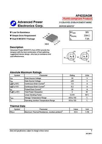
AP4232AGM RoHS-compliant Product Advanced Power N-CHANNEL ENHANCEMENT MODE Electronics Corp. POWER MOSFET Low On-Resistance BVDSS 30V D2 D2 Simple Drive Requirement RDS(ON) 23m D1 D1 Dual N MOSFET Package ID 7.8A G2 S2 G1 SO-8 S1 Description Advanced Power MOSFETs from APEC provide the D2 D1 designer with the best combination of fast switching, ruggedized devi
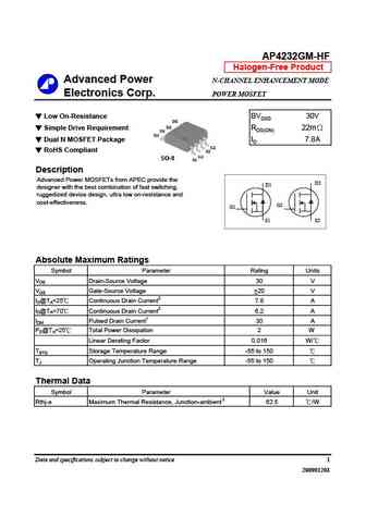
ap4232gm.pdf
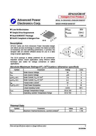
AP4232GM-HF Halogen-Free Product Advanced Power DUAL N-CHANNEL ENHANCEMENT Electronics Corp. MODE POWER MOSFET Low On-Resistance BVDSS 30V D2 D2 Simple Drive Requirement RDS(ON) 22m D1 D1 Dual N MOSFET Package ID 7.8A G2 RoHS Compliant & Halogen-Free S2 G1 SO-8 S1 Description AP4232 series are fro
ap4232bgm-hf.pdf

AP4232BGM-HF Halogen-Free Product Advanced Power DUAL N-CHANNEL ENHANCEMENT Electronics Corp. MODE POWER MOSFET Lower Gate Charge BVDSS 30V Simple Drive Requirement RDS(ON) 22m Fast Switching Characteristic ID 7.6A Halogen Free & RoHS Compliant Product D2 D2 D1 Description D1 Advanced Power MOSFETs from APEC provide the G2 S2 designer with the best combination o
ap4423gm-hf.pdf
AP4423GM-HF Halogen-Free Product Advanced Power P-CHANNEL ENHANCEMENT MODE Electronics Corp. POWER MOSFET Simple Drive Requirement BVDSS -30V D D D Low On-resistance RDS(ON) 15m D Fast Switching Characteristic ID -11A G S RoHS Compliant & Halogen-Free S S SO-8 Description D Advanced Power MOSFETs from APEC provide the designer with the best combination of f
ap4232gm-hf.pdf
AP4232GM-HF Halogen-Free Product Advanced Power N-CHANNEL ENHANCEMENT MODE Electronics Corp. POWER MOSFET Low On-Resistance BVDSS 30V D2 D2 Simple Drive Requirement RDS(ON) 22m D1 D1 Dual N MOSFET Package ID 7.8A G2 RoHS Compliant S2 G1 SO-8 S1 Description Advanced Power MOSFETs from APEC provide the D2 D1 designer with the best combination of fast switchi
am5423p.pdf
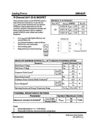
Analog Power AM5423P P-Channel 20-V (D-S) MOSFET These miniature surface mount MOSFETs utilize a PRODUCT SUMMARY high cell density trench process to provide low VDS (V) rDS(on) (OHM) ID (A) rDS(on) and to ensure minimal power loss and heat dissipation. Typical applications are DC-DC 0.024 @ VGS = -4.5V -8.4 converters and power management in portable and -20 0.031 @ VGS = -2.5V -7.4
am7423p.pdf
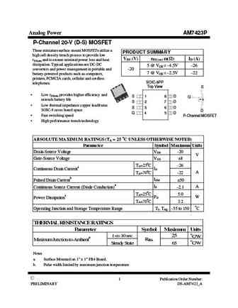
Analog Power AM7423P P-Channel 20-V (D-S) MOSFET These miniature surface mount MOSFETs utilize a PRODUCT SUMMARY high cell density trench process to provide low VDS (V) rDS(on) m( ) ID (A) rDS(on) and to ensure minimal power loss and heat dissipation. Typical applications are DC-DC 5 @ VGS = -4.5V -26 converters and power management in portable and -20 7 @ VGS = -2.5V -22 batte
ama423p.pdf
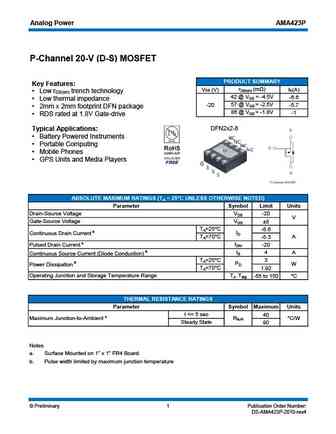
Analog Power AMA423P P-Channel 20-V (D-S) MOSFET PRODUCT SUMMARY Key Features rDS(on) (m ) VDS (V) ID(A) Low r trench technology DS(on) 42 @ VGS = -4.5V -6.6 Low thermal impedance -20 57 @ VGS = -2.5V -5.7 2mm x 2mm footprint DFN package 86 @ VGS = -1.8V -1 RDS rated at 1.8V Gate-drive DFN2x2-8 Typical Applications Battery Powered Instruments Portable
am3423p.pdf
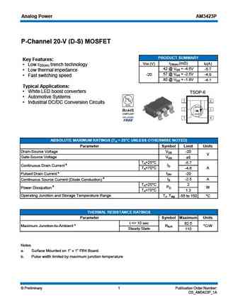
Analog Power AM3423P P-Channel 20-V (D-S) MOSFET PRODUCT SUMMARY Key Features rDS(on) (m ) VDS (V) ID(A) Low r trench technology DS(on) 42 @ VGS = -4.5V -5.7 Low thermal impedance -20 57 @ VGS = -2.5V -4.9 Fast switching speed 80 @ VGS = -1.8V -4.1 Typical Applications White LED boost converters TSOP-6 Automotive Systems Industrial DC/DC Conve
ao3423.pdf
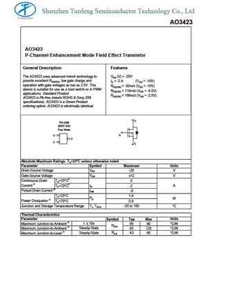
Shenzhen Tuofeng Semiconductor Technology Co., Ltd AO3423 AO3423 P-Channel Enhancement Mode Field Effect Transistor General Description Features The AO3423 uses advanced trench technology to VDS (V) = -20V provide excellent RDS(ON), low gate charge and ID = -2 A (VGS = -10V) operation with gate voltages as low as 2.5V. This RDS(ON)
bf423a3.pdf
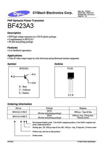
Spec. No. C235A3 Issued Date 2004.02.24 CYStech Electronics Corp. Revised Date 2014.04.01 Page No. 1/5 PNP Epitaxial Planar Transistor BF423A3 Description PNP high voltage transistors in a TO-92 plastic package. Complementary to BF422A3 Pb-free lead plating package Features Low feedback capacitance. Applications Class-B video output stages
mtp4423q8.pdf
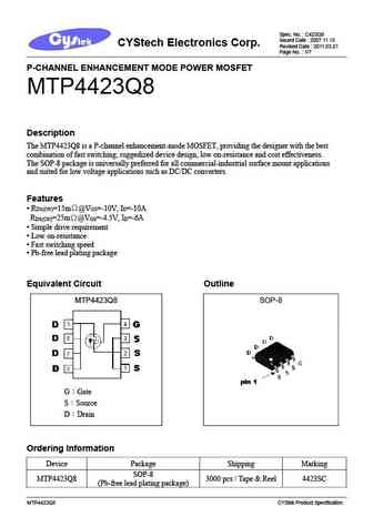
Spec. No. C423Q8 Issued Date 2007.11.15 CYStech Electronics Corp. Revised Date 2011.03.21 Page No. 1/7 P-CHANNEL ENHANCEMENT MODE POWER MOSFET MTP4423Q8 Description The MTP4423Q8 is a P-channel enhancement-mode MOSFET, providing the designer with the best combination of fast switching, ruggedized device design, low on-resistance and cost effectiveness. The SOP-8 pack
apm4230k.pdf
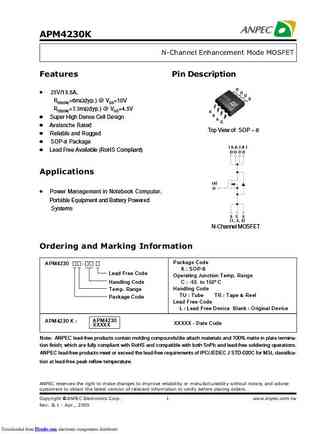
APM4230K N-Channel Enhancement Mode MOSFET Features Pin Description D 25V/13.5A, D D D RDS(ON)=6m (typ.) @ VGS=10V RDS(ON)=7.5m (typ.) @ VGS=4.5V S S Super High Dense Cell Design S G Avalanche Rated Top View of SOP - 8 Reliable and Rugged SOP-8 Package ( 5,6,7,8 ) L
stb423s stp423s.pdf
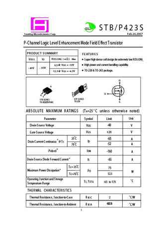
Green Product S T B / P 4 2 3 S S amHop Microelectronics C orp. Feb.26,2007 P-Channel Logic Level Enhancement Mode Field Effect Transistor PR ODUC T S UMMAR Y F E ATUR E S 4 R DS (ON) ( m ) Max VDS S ID S uper high dense cell design for extremely low R DS (ON) . 9.5 @ VG S = -10V High power and current handling capability. - 40V - 65A TO-220 & TO-263 package. 12.5 @ VG S
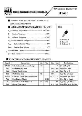
h423.pdf
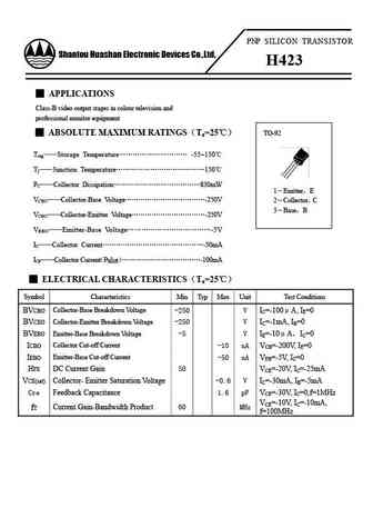
P NP S I L I C O N T R A N S I S T O R Shantou Huashan Electronic Devices Co.,Ltd. H423 APPLICATIONS Class-B video output stages in colour television and professional monitor equipment ABSOLUTE MAXIMUM RATINGS Ta=25 TO-92 Tstg Storage Temperature -55 150 Tj Junction Temperature 150
ko3423.pdf
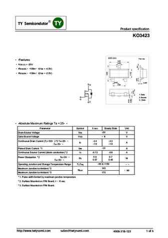
Product specification KO3423 SOT-23-3 Unit mm Features 2.9+0.2 -0.2 0.4+0.1 -0.05 VDS (V) = -20V 3 RDS(ON) 100m (VGS = -4.5V) RDS(ON) 150m (VGS = -2.5V) 12 +0.1 0.95-0.1 0.1+0.05 -0.01 +0.2 1.9-0.2 D 1. Gate 2. Source G 3. Drain S Absolute Maximum Ratings Ta = 25 Parameter Symbol 5 sec Steady State Unit Drain-Source Voltage
dwa401-dwa412 dwa417 dwa422 dwa423.pdf
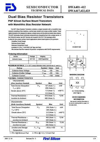
SEMICONDUCTOR DWA401 412 TECHNICAL DATA DWA417,422,423 Dual Bias Resistor Transistors PNP Silicon Surface Mount Transistors with Monolithic Bias Resistor Network The BRT (Bias Resistor Transistor) contains a single transistor with a monolithic bias network consisting of two resistors; a series base resistor and a base emitter resistor. These digital transistors are designed to replace
dta401-dta411 dta417 dta422-dta423.pdf
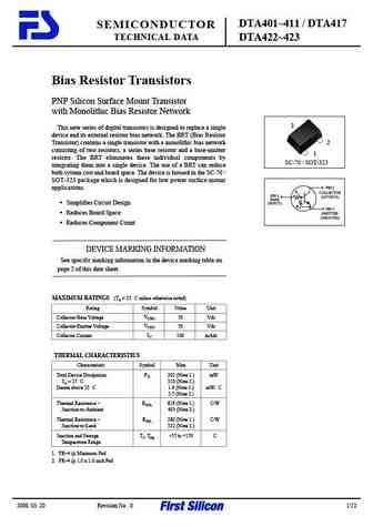
DTA401 411 / DTA417 SEMICONDUCTOR TECHNICAL DATA DTA422 423 Bias Resistor Transistors PNP Silicon Surface Mount Transistor with Monolithic Bias Resistor Network 3 This new series of digital transistors is designed to replace a single device and its external resistor bias network. The BRT (Bias Resistor Transistor) contains a single transistor with a monolithic bias network 2 consisti
ao3423.pdf
SMD Type AO3423 (KO3423) SOT-23 Unit mm +0.2 2.9-0.2 +0.1 0.4 -0.05 3 1 2 +0.1 +0.05 0.95 -0.1 0.1 -0.01 1.9+0.2 -0.2 D ESD Rating 2000V HBM G 1. Gate 2. Source 3. Drain S 0.4 +0.2 +0.2 2.8 -0.2 1.6 -0.1 0.55 +0.2 1.1 -0.1 +0.1 0-0.1 0.38 -0.1 SMD Type AO3423 (KO3423) Testconditions AS* SMD Type AO3423 (KO3423) 10 15 -10.0V -4.0V VDS=-5V -8
ao4423.pdf
SMD Type MOSFET P-Channel MOSFET AO4423 (KO4423) SOP-8 Features VDS (V) =-30V ID =-15 A (VGS =-20V) RDS(ON) 7m (VGS =-20V) 1.50 0.15 RDS(ON) 8.5m (VGS =-10V) RDS(ON) 12 m (VGS =- 6 V) 1 Source 5 Drain ESD Rating 3000V HBM 6 Drain 2 Source 7 Drain 3 Source 8 Drain 4 Gate D G S Absolute Maximum Ratings Ta = 25 Par
ao3423-3.pdf
SMD Type MOSFET P-Channel Enhancement MOSFET AO3423 (KO3423) SOT-23-3 Unit mm +0.2 2.9-0.1 +0.1 0.4 -0.1 3 Features VDS (V) =-20V ID =-2.0 A (VGS =-10V) D 1 2 RDS(ON) 92m (VGS =-10V) +0.02 +0.1 0.15 -0.02 0.95 -0.1 RDS(ON) 118m (VGS =-4.5V) +0.1 1.9 -0.2 RDS(ON) 166m (VGS =-2.5V) G 1. Gate 2. Source 3. Drain S Abso
2sd2423.pdf
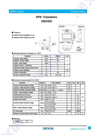
SMD Type Transistors NPN Transistors 2SD2423 SOT-89 Unit mm 1.70 0.1 Features Collector Current Capability IC=1.5A C Collector Emitter Voltage VCEO=50V 0.42 0.1 0.46 0.1 B ID 1.Base 2 k 0.5 2.Collector (Typ) (Typ) E 3.Emitter Absolute Maximum Ratings Ta = 25 Parameter Symbol Rating Unit Collector - Base Voltage VCBO 50 Collector - Emitter Volt
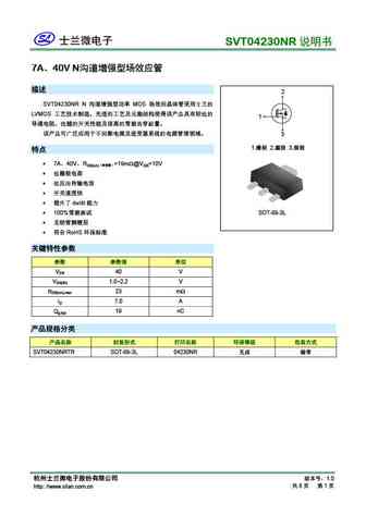
chm1423wgp.pdf
CHENMKO ENTERPRISE CO.,LTD CHM1423WGP SURFACE MOUNT N-Channel Enhancement Mode Field Effect Transistor VOLTAGE 20 Volts CURRENT 2.8 Ampere APPLICATION * Power Management in Note book * Portable Equipment * Battery Powered System * DC/DC Converter SC-70/SOT-323 * Load Switch * DSC * LCD Display inverter FEATURE 0.65 1.3 0.1 2.0 0.2 0.65 * Small surface mounting type. (SC-7
elm34423aa.pdf
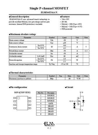
Single P-channel MOSFET ELM34423AA-N General description Features ELM34423AA-N uses advanced trench technology to Vds=-30V provide excellent Rds(on), low gate charge and low gate Id=-8A resistance. Internal ESD protection is included. Rds(on)
elm14423aa.pdf
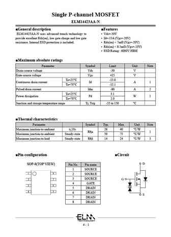
Single P-channel MOSFET ELM14423AA-N General description Features ELM14423AA-N uses advanced trench technology to Vds=-30V provide excellent Rds(on), low gate charge and low gate Id=-15A (Vgs=-20V) resistance. Internal ESD protection is included. Rds(on)
me7423s-g.pdf
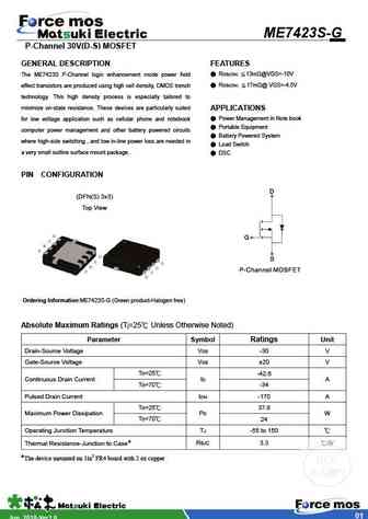
ME7423S-G P-Channel 30V(D-S) MOSFET D GENERAL DESCRIPTION FEATURES The ME7423S P-Channel logic enhancement mode power field RDS(ON) 13m @VGS=-10V effect transistors are produced using high cell density, DMOS trench RDS(ON) 17m @ VGS=-4.5V technology. This high density process is especially tailored to minimize on-state resistance. These devices are particularly
pmen2423s.pdf
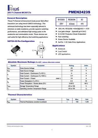
20V P-Channel MOSFETs PMEN2423S General Description BVDSS RDSON ID These P-Channel enhancement mode power field effect transistors are using trench DMOS technology. This -20V 43m -4A advanced technology has been especially tailored to -20V,-4A, RDS(ON) =43m @VGS = -4.5V minimize on-state resistance, provide superior switching Low gate charge (typicalQ gd 4.5nC) p
ssm4423gm.pdf
SSM4423GM P-CHANNEL ENHANCEMENT-MODE POWER MOSFET Simple drive requirement BV -30V DSS D D Lower gate charge R 15m DS(ON) D D Fast switching characteristics ID -11A G S S SO-8 S Description D Advanced Power MOSFETs from Silicon Standard provide the designer with the best combination of fast switching, G ruggedized device design, low on-resistance and cost-effectiveness.
ssm4232gm.pdf
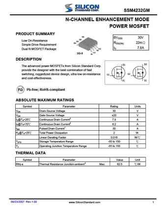
SSM4232GM N-CHANNEL ENHANCEMENT MODE POWER MOSFET PRODUCT SUMMARY D2 BVDSS 30V D2 Low On-Resistance D1 D1 RDS(ON) 22m Simple Drive Requirement ID 7.8A G2 Dual N MOSFET Package S2 G1 SO-8 S1 DESCRIPTION D2 D1 The advanced power MOSFETs from Silicon Standard Corp. provide the designer with the best combination of fast G2 switching, ruggedized device design, ultra
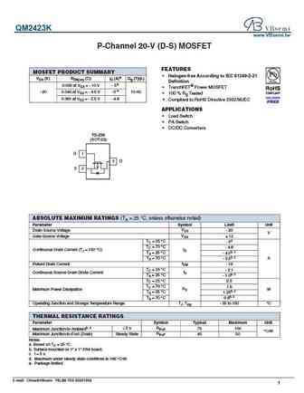
qm2423k.pdf
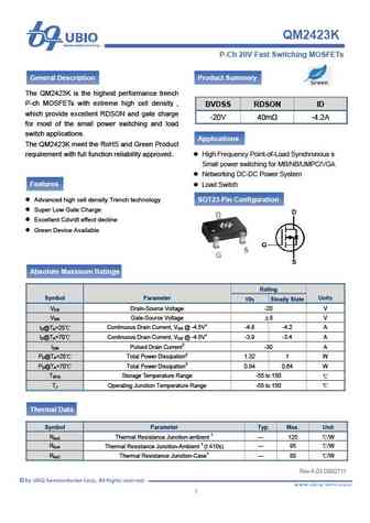
QM2423K P-Ch 20V Fast Switching MOSFETs General Description Product Summery The QM2423K is the highest performance trench P-ch MOSFETs with extreme high cell density , BVDSS RDSON ID which provide excellent RDSON and gate charge -20V 40m -4.2A for most of the small power switching and load switch applications. Applications The QM2423K meet the RoHS and Green Product requ
qm2423v.pdf
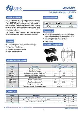
QM2423V P-Ch 20V Fast Switching MOSFETs General Description Product Summery The QM2423V is the highest performance trench P-ch MOSFETs with extreme high cell density , BVDSS RDSON ID which provide excellent RDSON and gate charge -20V 40m -4.5A for most of the small power switching and load switch applications. Applications The QM2423V meet the RoHS and Green Product requ
ao3423a.pdf
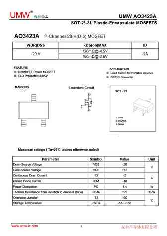
R UMW UMW AO3423A SOT-23-3L Plastic-Encapsulate MOSFETS P-Channel 20-V(D-S) MOSFET AO3423A V(BR)DSS RDS(on)MAX ID 120m @-4.5V -20 V -2A 150m @-2.5V FEATURE APPLICATION TrenchFET Power MOSFET Load Switch for Portable Devices ESD Protected 2.0KV DC/DC Converter MARKING Equivalent Circuit SOT 23 1. GATE 2. SOURCE 3. DRAIN Maximum ratings ( Ta=25 un
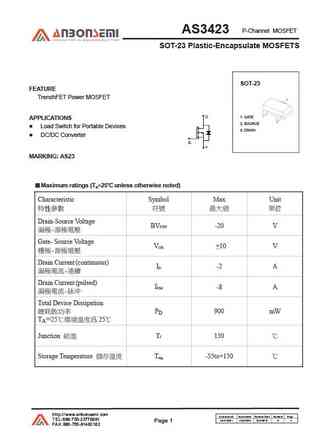
as3423.pdf
P-Channel MOSFET AS3423 SOT-23 Plastic-Encapsulate MOSFETS Dimensions In Millimeters Dimensions In Inches Symbol Min Max Min Max A 0.900 1.150 0.035 0.045 A1 0.000 0.100 0.000 0.004 A2 0.900 1.050 0.035 0.041 b 0.300 0.500 0.012 0.020 c 0.080 0.150 0.003 0.006 D 2.800 3.000 0.110 0.118 E 1.200 1.400 0.047 0.055 E1 2.250 2.550 0.089 0.100 e 0.
ao3423b.pdf
P-Channel MOSFET AO3423B SOT-23 Plastic-Encapsulate MOSFETS Dimensions In Millimeters Dimensions In Inches Symbol Min Max Min Max A 0.900 1.150 0.035 0.045 A1 0.000 0.100 0.000 0.004 A2 0.900 1.050 0.035 0.041 b 0.300 0.500 0.012 0.020 c 0.080 0.150 0.003 0.006 D 2.800 3.000 0.110 0.118 E 1.200 1.400 0.047 0.055 E1 2.250 2.550 0.089 0.100 e 0

as3423b.pdf
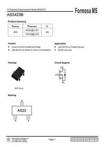
P-Channel Enhancement Mode MOSFET Formosa MS AS3423B Product Summary V(BR)DSS RDS(on)MAX ID 90m @-4.5V -20V -3A 110m @-2.5V Feature Application Advanced trench process technology Load Switch for Portable Devices High density cell design for ultra low on-resistance DC/DC Converter Package Circuit diagram SOT-23-3L Marking AS23 http //www.formosagr.com Document ID I


wst3423.pdf
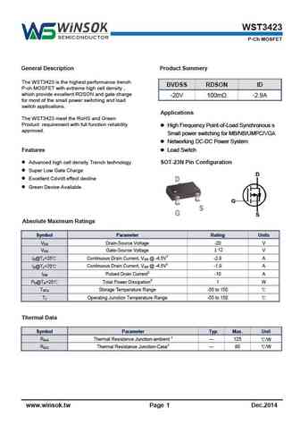
WST3423 P-Ch MOSFET General Description Product Summery The WST3423 is the highest performance trench BVDSS RDSON ID P-ch MOSFET with extreme high cell density , which provide excellent RDSON and gate charge -20V 100m -2.9A for most of the small power switching and load switch applications. Applications The WST3423 meet the RoHS and Green Product requirement with full fu
2sc4237t8tl.pdf
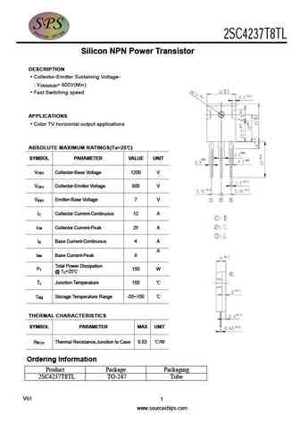
2SC4237T8TL Silicon NPN Power Transistor DESCRIPTION Collector-Emitter Sustaining Voltage- V = 800V(Min) CEO(SUS) Fast Switching speed APPLICATIONS Color TV horizontal output applications ABSOLUTE MAXIMUM RATINGS(Ta=25 ) SYMBOL PARAMETER VALUE UNIT V Collector-Base Voltage 1200 V CBO V Collector-Emitter Voltage 800 V CEO V Emitter-Base Voltage 7 V EBO I Collector Curr
ao3423.pdf
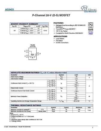
AO3423 www.VBsemi.tw P-Channel 20-V (D-S) MOSFET FEATURES MOSFET PRODUCT SUMMARY Halogen-free According to IEC 61249-2-21 VDS (V) RDS(on) ( )ID (A)a Qg (Typ.) Definition 0.035 at VGS = - 10 V - 5e TrenchFET Power MOSFET e - 20 0.043 at VGS = - 4.5 V - 5 10 nC 100 % Rg Tested 0.061 at VGS = - 2.5 V - 4.8 Compliant to RoHS Directive 2002/95/EC APPLICATIONS
ao4423.pdf
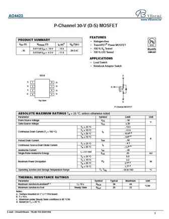
AO4423 www.VBsemi.tw P-Channel 30-V (D-S) MOSFET FEATURES PRODUCT SUMMARY Halogen-free VDS (V) RDS(on) ( ) ID (A)d Qg (Typ.) TrenchFET Power MOSFET 0.011 at VGS = - 10 V - 13.5 100 % Rg Tested RoHS - 30 29.5 nC COMPLIANT 100 % UIS Tested 0.015 at VGS = - 4.5 V - 11.6 APPLICATIONS Load Switch Notebook Adaptor Switch SO-8 S S 1 8 D S D 2 7 G S
si6423dq-t1.pdf
SI6423DQ-T1 www.VBsemi.tw P-Channel 20-V (G-S) MOSFET FEATURES PRODUCT SUMMARY Halogen-free VDS (V) RDS(on) ( )ID (A) Pb-free TrenchFET Power MOSFETs 0.012 at VGS = - 4.5 V Available - 9.0 RoHS* 0.015 at VGS = - 2.5 V -20 - 7.8 COMPLIANT 0.020 at VGS = - 1.8 V - 6.0 S* TSSOP-8 G D D 1 8 * Source Pins 2, 3, 6 and 7 S S must be tied common. 2 7 S S 3
hm4423.pdf
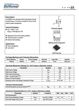
HM44 Description The HM44 uses advanced trench technology to provide excellent RDS(ON), This device is suitable for use as a load switch or power management. General Features Schematic diagram VDS = -30V,ID = -2 A RDS(ON)
2sc4237.pdf
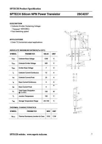
SPTECH Product Specification SPTECH Silicon NPN Power Transistor 2SC4237 DESCRIPTION Collector-Emitter Sustaining Voltage- V = 800V(Min) CEO(SUS) Fast Switching speed APPLICATIONS Color TV horizontal output applications ABSOLUTE MAXIMUM RATINGS(Ta=25 ) SYMBOL PARAMETER VALUE UNIT V Collector-Base Voltage 1200 V CBO V Collector-Emitter Voltage 800 V CEO V Emitter-Base Vo
2n6423.pdf
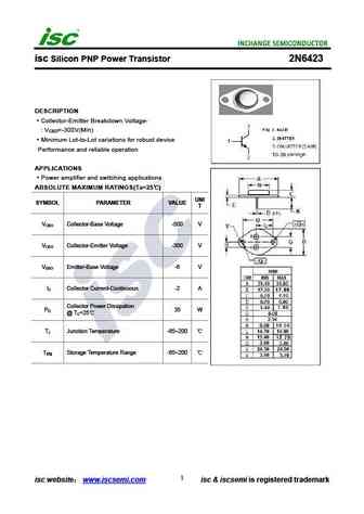
isc Silicon PNP Power Transistor 2N6423 DESCRIPTION Collector-Emitter Breakdown Voltage- V =-300V(Min) CEO Minimum Lot-to-Lot variations for robust device Performance and reliable operation APPLICATIONS Power amplifier and switching applications ABSOLUTE MAXIMUM RATINGS(Ta=25 ) UNI SYMBOL PARAMETER VALUE T V Collector-Base Voltage -500 V CBO V Collector-Emitter Voltage
aoi423.pdf
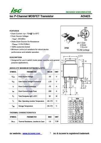
isc P-Channel MOSFET Transistor AOI423 FEATURES Drain Current I = -70A@ T =25 D C Drain Source Voltage- V = -30V(Min) DSS Static Drain-Source On-Resistance R = 8.5m (Max) DS(on) 100% avalanche tested Minimum Lot-to-Lot variations for robust device performance and reliable operation DESCRIPTION Designed for use in switch mode power supplies and general purpo
2sc4235.pdf
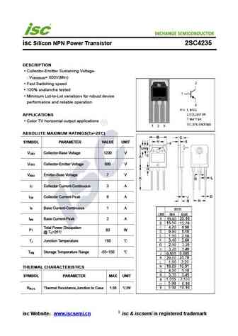
INCHANGE Semiconductor isc Silicon NPN Power Transistor 2SC4235 DESCRIPTION Collector-Emitter Sustaining Voltage- V = 800V(Min) CEO(SUS) Fast Switching speed 100% avalanche tested Minimum Lot-to-Lot variations for robust device performance and reliable operation APPLICATIONS Color TV horizontal output applications ABSOLUTE MAXIMUM RATINGS(Ta=25 ) SYMBOL PARAMETER VALU
2sc4231.pdf

INCHANGE Semiconductor isc Silicon NPN Power Transistor 2SC4231 DESCRIPTION Collector-Emitter Sustaining Voltage- V = 800V(Min) CEO(SUS) Fast Switching speed 100% avalanche tested Minimum Lot-to-Lot variations for robust device performance and reliable operation APPLICATIONS Electronic ballasts for fluorescent lighting Switch mode power supplies ABSOLUTE MAXIMUM RATIN
2sc3423-126.pdf
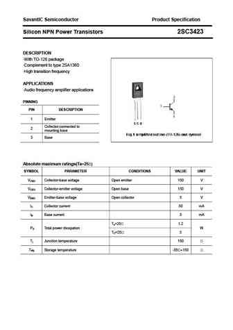
SavantIC Semiconductor Product Specification Silicon NPN Power Transistors 2SC3423 DESCRIPTION With TO-126 package Complement to type 2SA1360 High transition frequency APPLICATIONS Audio frequency amplifier applications PINNING PIN DESCRIPTION 1 Emitter Collector;connected to 2 mounting base 3 Base Absolute maximum ratings(Ta=25 ) SYMBOL PARAMETER CONDITION
2sc4233.pdf
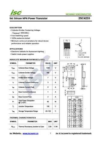
INCHANGE Semiconductor isc Silicon NPN Power Transistor 2SC4233 DESCRIPTION Collector-Emitter Sustaining Voltage- V = 800V(Min) CEO(SUS) Fast Switching speed 100% avalanche tested Minimum Lot-to-Lot variations for robust device performance and reliable operation APPLICATIONS Electronic ballasts for fluorescent lighting Switch mode power supplies ABSOLUTE MAXIMUM RATIN
aod423.pdf
INCHANGE Semiconductor isc P-Channel MOSFET Transistor AOD423 FEATURES With TO-252( DPAK ) packaging High speed switching Low gate input resistance Standard level gate drive Easy to use 100% avalanche tested Minimum Lot-to-Lot variations for robust device performance and reliable operation APPLICATIONS Power supply Switching applications ABSOLUTE MAXIMUM RA
aoy423.pdf
INCHANGE Semiconductor isc P-Channel MOSFET Transistor AOY423 FEATURES With TO-251(IPAK) packaging High speed switching Easy to use 100% avalanche tested Minimum Lot-to-Lot variations for robust device performance and reliable operation APPLICATIONS Power supply DC-DC converters Motor control Switching applications ABSOLUTE MAXIMUM RATINGS(T =25 ) a SYM
2sc4234.pdf
INCHANGE Semiconductor isc Silicon NPN Power Transistor 2SC4234 DESCRIPTION Collector-Emitter Sustaining Voltage- V = 800V(Min) CEO(SUS) Fast Switching speed 100% avalanche tested Minimum Lot-to-Lot variations for robust device performance and reliable operation APPLICATIONS Electronic ballasts for fluorescent lighting Switch mode power supplies ABSOLUTE MAXIMUM RATIN
2n4231.pdf
isc Silicon NPN Power Transistor 2N4231 DESCRIPTION Excellent Safe Operating Area Low Collector-Emitter Saturation Voltage 100% avalanche tested Minimum Lot-to-Lot variations for robust device performance and reliable operation. APPLICATIONS Designed for general-purpose power amplifier and switching applications ABSOLUTE MAXIMUM RATINGS(T =25 ) a SYMBOL PARAMETER VALUE U
2sc4236.pdf

INCHANGE Semiconductor isc Silicon NPN Power Transistor 2SC4236 DESCRIPTION Collector-Emitter Sustaining Voltage- V = 800V(Min) CEO(SUS) Fast Switching speed 100% avalanche tested Minimum Lot-to-Lot variations for robust device performance and reliable operation APPLICATIONS Color TV horizontal output applications ABSOLUTE MAXIMUM RATINGS(T =25 ) a SYMBOL PARAMETER V
2n4232a.pdf

isc Silicon NPN Power Transistor 2N4232A DESCRIPTION Excellent Safe Operating Area Low Collector-Emitter Saturation Voltage 100% avalanche tested Minimum Lot-to-Lot variations for robust device performance and reliable operation. APPLICATIONS Designed for general-purpose power amplifier and switching applications ABSOLUTE MAXIMUM RATINGS(T =25 ) a SYMBOL PARAMETER VALUE
2sc4232.pdf
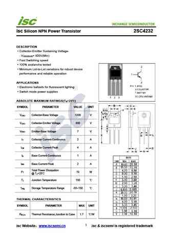
INCHANGE Semiconductor isc Silicon NPN Power Transistor 2SC4232 DESCRIPTION Collector-Emitter Sustaining Voltage- V = 800V(Min) CEO(SUS) Fast Switching speed 100% avalanche tested Minimum Lot-to-Lot variations for robust device performance and reliable operation APPLICATIONS Electronic ballasts for fluorescent lighting Switch mode power supplies ABSOLUTE MAXIMUM RATIN
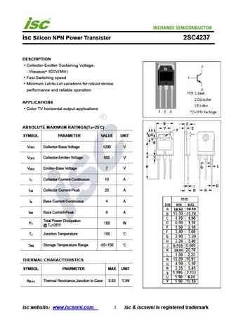
2sc4423.pdf
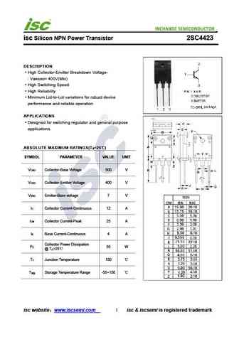
isc Silicon NPN Power Transistor 2SC4423 DESCRIPTION High Collector-Emitter Breakdown Voltage- V = 400V(Min) (BR)CEO High Switching Speed High Reliability Minimum Lot-to-Lot variations for robust device performance and reliable operation APPLICATIONS Designed for switching regulator and general purpose applications. ABSOLUTE MAXIMUM RATINGS(T =25 ) a SYMBOL PARAMETER
2sc4230.pdf
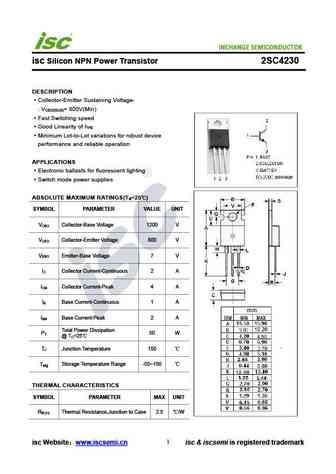
INCHANGE Semiconductor isc Silicon NPN Power Transistor 2SC4230 DESCRIPTION Collector-Emitter Sustaining Voltage- V = 800V(Min) CEO(SUS) Fast Switching speed Good Linearity of h FE Minimum Lot-to-Lot variations for robust device performance and reliable operation APPLICATIONS Electronic ballasts for fluorescent lighting Switch mode power supplies ABSOLUTE MAXIMUM RAT
2sc3423.pdf
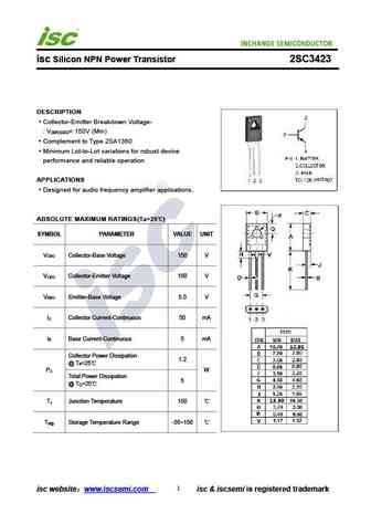
isc Silicon NPN Power Transistor 2SC3423 DESCRIPTION Collector-Emitter Breakdown Voltage- V = 150V (Min) (BR)CEO Complement to Type 2SA1360 Minimum Lot-to-Lot variations for robust device performance and reliable operation APPLICATIONS Designed for audio frequency amplifier applications. ABSOLUTE MAXIMUM RATINGS(Ta=25 ) SYMBOL PARAMETER VALUE UNIT V Collector-Base Voltag
2n4233a.pdf

isc Silicon NPN Power Transistor 2N4233A DESCRIPTION Excellent Safe Operating Area Low Collector-Emitter Saturation Voltage 100% avalanche tested Minimum Lot-to-Lot variations for robust device performance and reliable operation. APPLICATIONS Designed for general-purpose power amplifier and switching applications ABSOLUTE MAXIMUM RATINGS(T =25 ) a SYMBOL PARAMETER VALUE
mj423.pdf
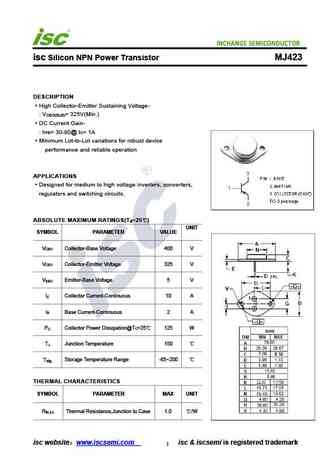
isc Silicon NPN Power Transistor MJ423 DESCRIPTION High Collector-Emitter Sustaining Voltage- V = 325V(Min.) CEO(SUS) DC Current Gain- h = 30-90@ I = 1A FE C Minimum Lot-to-Lot variations for robust device performance and reliable operation APPLICATIONS Designed for medium to high voltage inverters, converters, regulators and switching circuits. ABSOLUTE MAXIMUM RATINGS
2sc4237.pdf
isc Silicon NPN Power Transistor 2SC4237 DESCRIPTION Collector-Emitter Sustaining Voltage- V = 800V(Min) CEO(SUS) Fast Switching speed Minimum Lot-to-Lot variations for robust device performance and reliable operation APPLICATIONS Color TV horizontal output applications ABSOLUTE MAXIMUM RATINGS(Ta=25 ) SYMBOL PARAMETER VALUE UNIT V Collector-Base Voltage 1200 V CBO V C
2sk2423.pdf
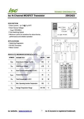
isc N-Channel MOSFET Transistor 2SK2423 DESCRIPTION Drain Current I = 7A@ T =25 D C Drain Source Voltage- V = 450V(Min) DSS Fast Switching Speed Minimum Lot-to-Lot variations for robust device performance and reliable operation APPLICATIONS Switching Regulators DC-DC Converter, Motor Control ABSOLUTE MAXIMUM RATINGS(T =25 ) a SYMBOL ARAMETER VALUE UNIT V Dr
Другие транзисторы: 41500, 41501, 41502, 41503, 41504, 41505, 41506, 41508, 2SC2655, 431, 43104, 45190, 45191, 45192, 45193, 45194, 45195
History: CFC3852
🌐 : EN ES РУ

Список транзисторов
Обновления
BJT: GA1A4M | SBT42 | 2SA200-Y | 2SA200-O | 2SD882-Q | 2SD882-P | 2SD882-E | 2SC945-L | 2SC945-H | 2SC4226-R23 | 2SC3357-F | 2SC3357-E | 2SC3356-R26 | 2SC3356-R24 | 2SC3356-R23 | 2SB772-Q | 2SB772-P | 2SB772-E | 2SA1015-L | 2SA1015-H | HSS8550
Popular searches
kn2907a | ncep028n85 datasheet | sw50n06 | 2sa1232 | 2sc1940 | ftp08n06a | 2n3405 | 2n3567