431 datasheet, аналоги, основные параметры
Наименование производителя: 431 📄📄
Тип материала: Si
Полярность: NPN
Предельные значения
Максимальная рассеиваемая мощность (Pc): 125 W
Макcимально допустимое напряжение коллектор-база (Ucb): 400 V
Макcимально допустимое напряжение коллектор-эмиттер (Uce): 325 V
Макcимально допустимое напряжение эмиттер-база (Ueb): 5 V
Макcимальный постоянный ток коллектора (Ic): 7 A
Предельная температура PN-перехода (Tj): 150 °C
Электрические характеристики
Граничная частота коэффициента передачи тока (ft): 4 MHz
Статический коэффициент передачи тока (hFE): 40
Корпус транзистора: TO3
📄📄 Копировать
Аналоги (замена) для 431
- подборⓘ биполярного транзистора по параметрам
431 даташит
irfb4310gpbf.pdf
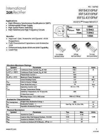
PD - 96190 IRFB4310GPbF Applications HEXFET Power MOSFET l High Efficiency Synchronous Rectification in SMPS l Uninterruptible Power Supply D VDSS 100V l High Speed Power Switching l Hard Switched and High Frequency Circuits RDS(on) typ. 5.6m G max. 7.0m ID 130A S Benefits l Improved Gate, Avalanche and Dynamic dV/dt Ruggedness l Fully Characterized Capacitance and Avalanche
irfb4310zpbf irfs4310zpbf irfsl4310zpbf.pdf
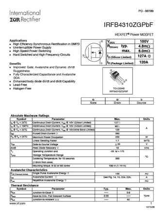
PD - 97115D IRFB4310ZPbF IRFS4310ZPbF IRFSL4310ZPbF HEXFET Power MOSFET Applications D VDSS 100V l High Efficiency Synchronous Rectification in SMPS RDS(on) typ. 4.8m l Uninterruptible Power Supply l High Speed Power Switching max. 6.0m l Hard Switched and High Frequency Circuits G ID (Silicon Limited) 127A c ID (Package Limited) 120A S Benefits l Improved Gate,
irfl4310pbf.pdf
PD - 95144 IRFL4310PbF HEXFET Power MOSFET D Surface Mount VDSS = 100V Dynamic dv/dt Rating Fast Switching Ease of Paralleling RDS(on) = 0.20 Advanced Process Technology G Ultra Low On-Resistance ID = 1.6A Lead-Free S Description Fifth Generation HEXFETs from International Rectifier utilize advanced processing techniques to achieve extremely low on-resistance per
irfl4315pbf.pdf

PD - 95258A IRFL4315PbF HEXFET Power MOSFET VDSS RDS(on) max ID Applications l High frequency DC-DC converters 150V 185mW@VGS = 10V 2.6A Benefits l Low Gate to Drain Charge to Reduce Switching Losses l Fully Characterized Capacitance Including Effective COSS to Simplify Design, (See App. Note AN1001) SOT-223 l Fully Characterized Avalanche Voltage and Current l Lead-Free Abs
irfb4310pbf irfs4310pbf irfsl4310pbf.pdf
PD - 14275D IRFB4310PbF IRFS4310PbF IRFSL4310PbF Applications HEXFET Power MOSFET l High Efficiency Synchronous Rectification in SMPS l Uninterruptible Power Supply D VDSS 100V l High Speed Power Switching l Hard Switched and High Frequency Circuits RDS(on) typ. 5.6m G max. 7.0m ID 130A S Benefits l Improved Gate, Avalanche and Dynamic dV/dt Ruggedness l Fully Characterized
irfb4310zgpbf.pdf
PD - 96189 IRFB4310ZGPbF HEXFET Power MOSFET Applications D VDSS 100V l High Efficiency Synchronous Rectification in SMPS RDS(on) typ. 4.8m l Uninterruptible Power Supply l High Speed Power Switching max. 6.0m l Hard Switched and High Frequency Circuits G ID (Silicon Limited) 127A ID (Package Limited) 120A S Benefits l Improved Gate, Avalanche and Dynamic dV/dt D Ruggedn
irfp4310zpbf.pdf
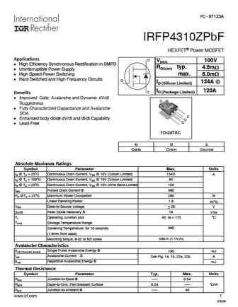
PD - 97123A IRFP4310ZPbF HEXFET Power MOSFET Applications D VDSS 100V l High Efficiency Synchronous Rectification in SMPS RDS(on) typ. 4.8m l Uninterruptible Power Supply l High Speed Power Switching max. 6.0m l Hard Switched and High Frequency Circuits G ID (Silicon Limited) 134A c ID (Package Limited) 120A S Benefits l Improved Gate, Avalanche and Dynamic dV/dt
auirfs4310trl.pdf
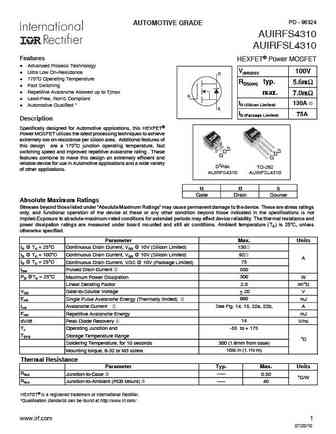
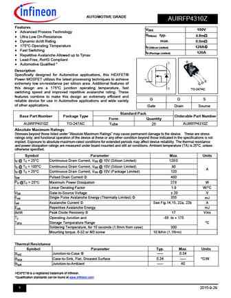
PD - 96324 AUTOMOTIVE GRADE AUIRFS4310 AUIRFSL4310 Features HEXFET Power MOSFET l Advanced Process Technology V(BR)DSS l Ultra Low On-Resistance 100V D l 175 C Operating Temperature RDS(on) typ. 5.6m l Fast Switching l Repetitive Avalanche Allowed up to Tjmax max. 7.0m G l Lead-Free, RoHS Compliant ID (Silicon Limited) 130A l Automotive Qualified * S ID (Package L
irfl4315.pdf
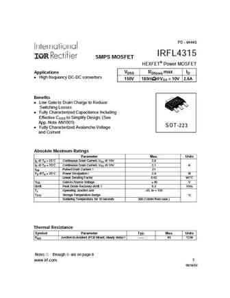
PD - 94445 IRFL4315 SMPS MOSFET HEXFET Power MOSFET VDSS RDS(on) max ID Applications High frequency DC-DC converters 150V 185m @VGS = 10V 2.6A Benefits Low Gate to Drain Charge to Reduce Switching Losses Fully Characterized Capacitance Including Effective COSS to Simplify Design, (See App. Note AN1001) SOT-223 Fully Characterized Avalanche Voltage an
irfl4310.pdf
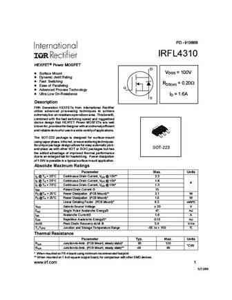
PD - 91368B IRFL4310 HEXFET Power MOSFET D VDSS = 100V l Surface Mount l Dynamic dv/dt Rating l Fast Switching RDS(on) = 0.20W l Ease of Paralleling G l Advanced Process Technology l Ultra Low On-Resistance ID = 1.6A S Description Fifth Generation HEXFETs from International Rectifier utilize advanced processing techniques to achieve extremely low on-resistance per silicon ar
auirfp4310z.pdf
AUTOMOTIVE GRADE AUIRFP4310Z Features VDSS 100V Advanced Process Technology RDS(on) typ. 4.8m Ultra Low On-Resistance max. Dynamic dv/dt Rating 6.0m 175 C Operating Temperature ID (Silicon Limited) 128A Fast Switching ID (Package Limited) 120A Repetitive Avalanche Allowed up to Tjmax Lead-Free, RoHS Compliant D Autom
2sc4315.pdf
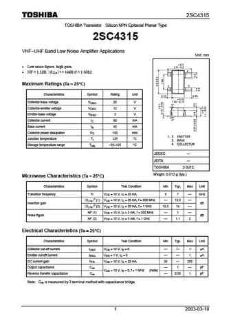
2SC4315 TOSHIBA Transistor Silicon NPN Epitaxial Planar Type 2SC4315 VHF UHF Band Low Noise Amplifier Applications Unit mm Low noise figure, high gain. NF = 1.1dB, S 2 = 14dB (f = 1 GHz) 21e Maximum Ratings (Ta = = 25 C) = = Characteristics Symbol Rating Unit Collector-base voltage VCBO 20 V Collector-emitter voltage VCEO 12 V Emitter-base voltage VEBO 3 V C
2sc4317.pdf
2SC4317 TOSHIBA Transistor Silicon NPN Epitaxial Planar Type 2SC4317 VHF UHF Band Low Noise Amplifier Applications Unit mm Low noise figure, high gain. NF = 1.1dB, S 2 = 13dB (f = 1 GHz) 21e Maximum Ratings (Ta = = 25 C) = = Characteristics Symbol Rating Unit Collector-base voltage VCBO 20 V Collector-emitter voltage VCEO 10 V Emitter-base voltage VEBO 1.5 V
mch6431.pdf
MCH6431 Ordering number ENA1852 SANYO Semiconductors DATA SHEET N-Channel Silicon MOSFET General-Purpose Switching Device MCH6431 Applications Features ON-resistance RDS(on)1=42m (typ.) 4V drive Halogen free compliance. Specifications at Ta=25 C Absolute Maximum Ratings Parameter Symbol Conditions Ratings Unit Drain-to-Source Voltage VDSS 30 V Gate-to-Sour
2sk1431.pdf
Ordering number EN3569 N-Channel Silicon MOSFET 2SK1431 Ultrahigh-Speed Switching Applications Features Package Dimensions Low ON-state resistance. unit mm Ultrahigh-speed switching. 2063A Converters. [2SK1431] Micaless package facilitating easy mounting. 4.5 10.0 2.8 3.2 2.4 1.6 1.2 0.7 0.75 1 2 3 1 Gate 2.55 2.55 2 Drain 3 Source 2.55 2.55 SANYO
sft1431.pdf
SFT1431 Ordering number ENA1624 SANYO Semiconductors DATA SHEET N-Channel Silicon MOSFET General-Purpose Switching Device SFT1431 Applications Features Motor drive application. Low ON-resistance. 4V drive. Specifications at Ta=25 C Absolute Maximum Ratings Parameter Symbol Conditions Ratings Unit Drain-to-Source Voltage VDSS 35 V Gate-to-Source Voltage VGSS 20
r07ds0431ej 2sc1213a-1.pdf
Preliminary Datasheet R07DS0431EJ0300 2SC1213, 2SC1213A (Previous REJ03G0684-0200) Rev.3.00 Silicon NPN Epitaxial Jun 07, 2011 Application Low frequency amplifier Complementary pair with 2SA673 and 2SA673A Outline RENESAS Package code PRSS0003DA-A (Package name TO-92 (1)) 1. Emitter 2. Collector 3. Base 3 2 1 Absolute Maximum Ratings (Ta = 25 C) Item S
2sk3431-s-z-zj.pdf
To our customers, Old Company Name in Catalogs and Other Documents On April 1st, 2010, NEC Electronics Corporation merged with Renesas Technology Corporation, and Renesas Electronics Corporation took over all the business of both companies. Therefore, although the old company name remains in this document, it is a valid Renesas Electronics document. We appreciate your understanding.
fjn4312r.pdf
FJN4312R Switching Application (Bias Resistor Built In) Switching circuit, Inverter, Interface circuit, Driver Circuit Built in bias Resistor (R=47K ) Complement to FJN3312R TO-92 1 1. Emitter 2. Collector 3. Base PNP Epitaxial Silicon Transistor Absolute Maximum Ratings Ta=25 C unless otherwise noted Equivalent Circuit C Symbol Parameter Value Units VCBO Collector-
fjn4310r.pdf
FJN4310R Switching Application (Bias Resistor Built In) Switching circuit, Inverter, Interface circuit, Driver Circuit Built in bias Resistor (R=10K ) Complement to FJN3310R TO-92 1 1. Emitter 2. Collector 3. Base PNP Epitaxial Silicon Transistor Absolute Maximum Ratings Ta=25 C unless otherwise noted Equivalent Circuit C Symbol Parameter Value Units VCBO Collector-
fjn4313r.pdf

FJN4313R Switching Application (Bias Resistor Built In) Switching circuit, Inverter, Interface circuit, Driver Circuit Built in bias Resistor (R1=2.2K , R2=47K ) Complement to FJN3313R TO-92 1 1. Emitter 2. Collector 3. Base PNP Epitaxial Silicon Transistor Absolute Maximum Ratings Ta=25 C unless otherwise noted Equivalent Circuit Symbol Parameter Value Units C VCB
2sc5200 fjl4315.pdf

January 2009 2SC5200/FJL4315 NPN Epitaxial Silicon Transistor Applications High-Fidelity Audio Output Amplifier General Purpose Power Amplifier Features High Current Capability IC = 17A. TO-264 1 High Power Dissipation 150watts. High Frequency 30MHz. 1.Base 2.Collector 3.Emitter High Voltage VCEO=250V Wide S.O.A for reliable operation. Excel
fjn4311r.pdf
FJN4311R Switching Application (Bias Resistor Built In) Switching circuit, Inverter, Interface circuit, Driver Circuit Built in bias Resistor (R=22K ) Complement to FJN3311R TO-92 1 1. Emitter 2. Collector 3. Base PNP Epitaxial Silicon Transistor Absolute Maximum Ratings Ta=25 C unless otherwise noted Equivalent Circuit Symbol Parameter Value Units C VCBO Collector-
fja4313.pdf
FJA4313 Audio Power Amplifier High Current Capability IC=15A High Power Dissipation Wide S.O.A Complement to FJA4213 TO-3P 1 1.Base 2.Collector 3.Emitter NPN Epitaxial Silicon Transistor Absolute Maximum Ratings TC=25 C unless otherwise noted Symbol Parameter Value Units VCBO Collector-Base Voltage 230 V VCEO Collector-Emitter Voltage 230 V VEBO Emitter-Base
fjaf4310.pdf
FJAF4310 Audio Power Amplifier High Current Capability IC=10A High Power Dissipation Wide S.O.A Complement to FJAF4210 TO-3PF 1 1.Base 2.Collector 3.Emitter NPN Epitaxial Silicon Transistor Absolute Maximum Ratings TC=25 C unless otherwise noted Symbol Parameter Value Units VCBO Collector-Base Voltage 200 V VCEO Collector-Emitter Voltage 140 V VEBO Emitter-Base
fjn4314r.pdf
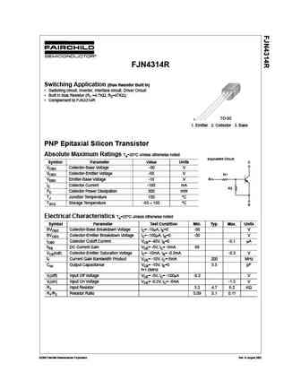
FJN4314R Switching Application (Bias Resistor Built In) Switching circuit, Inverter, Interface circuit, Driver Circuit Built in bias Resistor (R1 =4.7K , R2=47K ) Complement to FJN3314R TO-92 1 1. Emitter 2. Collector 3. Base PNP Epitaxial Silicon Transistor Absolute Maximum Ratings Ta=25 C unless otherwise noted Equivalent Circuit Symbol Parameter Value Units C VC
fds9431a.pdf
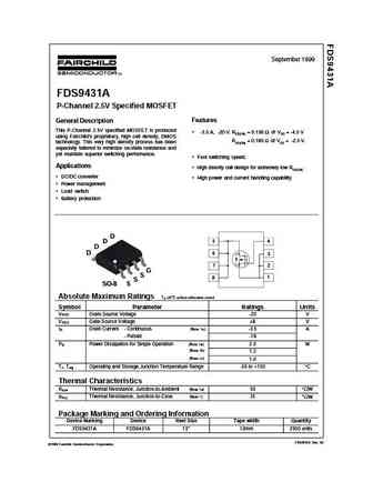
September 1999 FDS9431A P-Channel 2.5V Specified MOSFET Features General Description This P-Channel 2.5V specified MOSFET is produced -3.5 A, -20 V. RDS(ON) = 0.130 @ VGS = -4.5 V using Fairchild's proprietary, high cell density, DMOS RDS(ON) = 0.180 @ VGS = -2.5 V. technology. This very high density process has been especially tailored to minimize on-state resistance and
fja4310.pdf
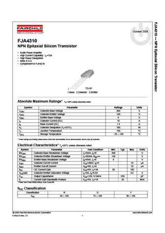
October 2008 FJA4310 NPN Epitaxial Silicon Transistor Audio Power Amplifier High Current Capability IC=10A High Power Dissipation Wide S.O.A Complement to FJA4210 TO-3P 1 1.Base 2.Collector 3.Emitter Absolute Maximum Ratings* Ta = 25 C unless otherwise noted Symbol Parameter Ratings Units VCBO Collector-Base Voltage 200 V VCEO Collector-Emitter Voltage 140 V
2sc5242 fja4313.pdf
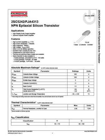
January 2009 2SC5242/FJA4313 NPN Epitaxial Silicon Transistor Applications High-Fidelity Audio Output Amplifier General Purpose Power Amplifier Features High Current Capability IC = 17A TO-3P 1 High Power Dissipation 130watts 1.Base 2.Collector 3.Emitter High Frequency 30MHz. High Voltage VCEO=250V Wide S.O.A for reliable operation. Excelle
fds9431a f085.pdf
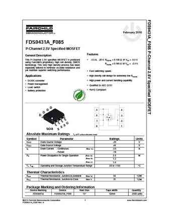
February 2010 tm FDS9431A_F085 P-Channel 2.5V Specified MOSFET Features General Description This P-Channel 2.5V specified MOSFET is produced -3.5 A, -20 V. RDS(ON) = 0.130 @ VGS = -4.5 V using Fairchild's proprietary, high cell density, DMOS RDS(ON) = 0.180 @ VGS = -2.5 V. technology. This very high density process has been especially tailored to minimize on-state resistan
fjl4315.pdf
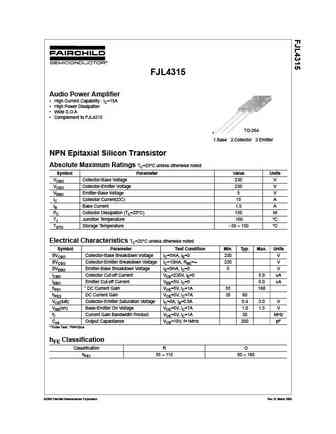
FJL4315 Audio Power Amplifier High Current Capability IC=15A High Power Dissipation Wide S.O.A Complement to FJL4215 TO-264 1 1.Base 2.Collector 3.Emitter NPN Epitaxial Silicon Transistor Absolute Maximum Ratings TC=25 C unless otherwise noted Symbol Parameter Value Units VCBO Collector-Base Voltage 230 V VCEO Collector-Emitter Voltage 230 V VEBO Emitter-Base
2sc5431.pdf
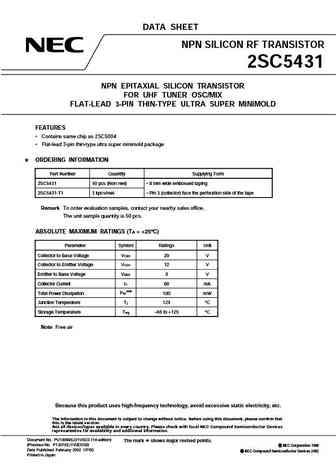
DATA SHEET NPN SILICON RF TRANSISTOR 2SC5431 NPN EPITAXIAL SILICON TRANSISTOR FOR UHF TUNER OSC/MIX FLAT-LEAD 3-PIN THIN-TYPE ULTRA SUPER MINIMOLD FEATURES Contains same chip as 2SC5004 Flat-lead 3-pin thin-type ultra super minimold package ORDERING INFORMATION Part Number Quantity Supplying Form 2SC5431 50 pcs (Non reel) 8 mm wide embossed taping 2SC5431-T1 3 kpcs/reel
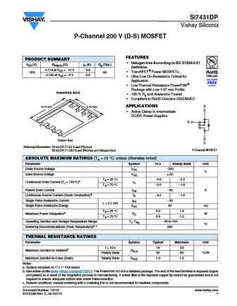
sia431dj.pdf
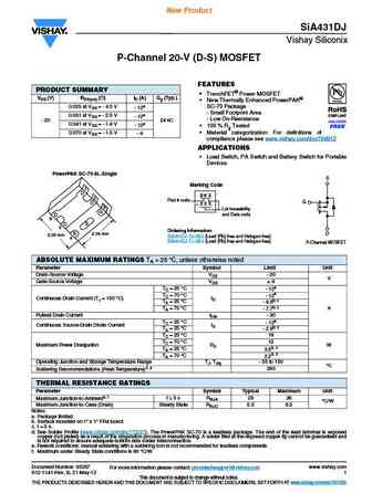
New Product SiA431DJ Vishay Siliconix P-Channel 20-V (D-S) MOSFET FEATURES PRODUCT SUMMARY TrenchFET Power MOSFET VDS (V) RDS(on) ( )ID (A) Qg (Typ.) New Thermally Enhanced PowerPAK 0.025 at VGS = - 4.5 V SC-70 Package - 12a - Small Footprint Area 0.031 at VGS = - 2.5 V - 12a - Low On-Resistance - 20 24 nC 0.041 at VGS = - 1.8 V - 12a 100 % Rg Tested 0
u430 u431.pdf
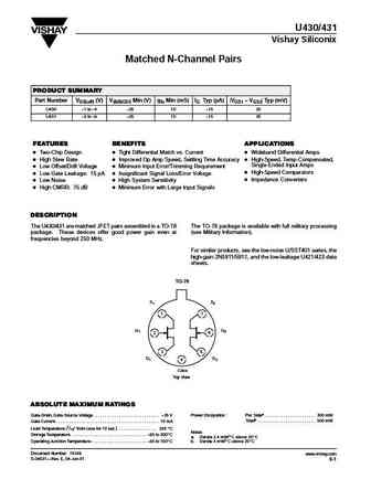
U430/431 Vishay Siliconix Matched N-Channel Pairs PRODUCT SUMMARY Part Number VGS(off) (V) V(BR)GSS Min (V) gfs Min (mS) IG Typ (pA) jVGS1 VGS2j Typ (mV) U430 1 to 4 25 10 15 25 U431 2 to 6 25 10 15 25 FEATURES BENEFITS APPLICATIONS D Two-Chip Design D Tight Differential Match vs. Current D Wideband Differential Amps D High Slew Rate D Improved Op Amp Speed,
si1431dh.pdf
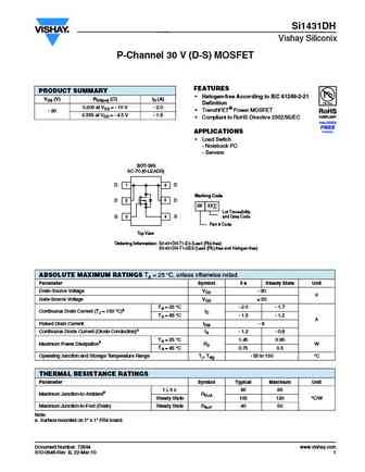
Si1431DH Vishay Siliconix P-Channel 30 V (D-S) MOSFET FEATURES PRODUCT SUMMARY Halogen-free According to IEC 61249-2-21 VDS (V) RDS(on) ( )ID (A) Definition 0.200 at VGS = - 10 V - 2.0 TrenchFET Power MOSFET - 30 0.355 at VGS = - 4.5 V - 1.6 Compliant to RoHS Directive 2002/95/EC APPLICATIONS Load Switch - Notebook PC - Servers SOT-363 SC-70 (6-LEADS)
si4310bd.pdf
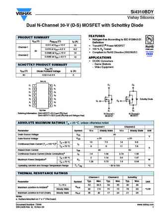
Si4310BDY Vishay Siliconix Dual N-Channel 30-V (D-S) MOSFET with Schottky Diode FEATURES PRODUCT SUMMARY Halogen-free According to IEC 61249-2-21 VDS (V) RDS(on) ( ) ID (A) Definition 0.011 at VGS = 10 V 10 TrenchFET Power MOSFET Channel-1 0.016 at VGS = 4.5 V 8.2 100 % Rg Tested 30 Compliant to RoHS Directive 2002/95/EC 0.0085 at VGS = 10 V 14 Chann
sqj431ep.pdf
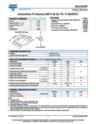
SQJ431EP www.vishay.com Vishay Siliconix Automotive P-Channel 200 V (D-S) 175 C MOSFET FEATURES PRODUCT SUMMARY Halogen-free According to IEC 61249-2-21 VDS (V) - 200 Definition RDS(on) ( ) at VGS = - 10 V 0.213 TrenchFET Power MOSFET RDS(on) ( ) at VGS = - 6 V 0.221 AEC-Q101 Qualifiedd ID (A) - 12 100 % Rg and UIS Tested Configuration Single Complian
si4431ady.pdf
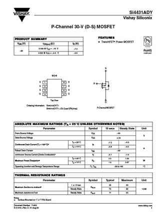
Si4431ADY Vishay Siliconix P-Channel 30-V (D-S) MOSFET FEATURES PRODUCT SUMMARY D TrenchFETr Power MOSFET VDS (V) rDS(on) (W) ID (A) 0.030 @ VGS = 10 V 7.2 30 30 0.052 @ VGS = 4.5 V 5.5 S SO-8 SD 1 8 G S D 2 7 SD 3 6 G D 4 5 Top View D Ordering Information Si4431ADY-T1 P-Channel MOSFET Si4431ADY-T1 E3 (Lead (Pb)-free) ABSOLUTE MAXIMUM RATINGS (TA
si4431dy.pdf
Si4431DY Vishay Siliconix P-Channel 30-V (D-S) MOSFET FEATURES PRODUCT SUMMARY D TrenchFETr Power MOSFET VDS (V) rDS(on) (W) ID (A) D 100% UIS Tested 0.040 @ VGS = 10 V "5.8 30 30 0.070 @ VGS = 4.5 V "4.5 S SO-8 SD 1 8 G S D 2 7 SD 3 6 G D 4 5 Top View D Ordering Information Si4431DY-T1 P-Channel MOSFET Si4431DY-T1 E3 (Lead (Pb)-Free) ABSOLUTE MAXIMUM RAT
si4431bd.pdf

Si4431BDY Vishay Siliconix P-Channel 30-V (D-S) MOSFET FEATURES PRODUCT SUMMARY Halogen-free According to IEC 61249-2-21 VDS (V) RDS(on) ( )ID (A) Available 0.030 at VGS = - 10 V - 7.5 TrenchFET Power MOSFETs - 30 0.050 at VGS = - 4.5 V - 5.8 SO-8 S 1 8 D S S D 2 7 S 3 6 D G G D 4 5 Top View D Ordering Information Si4431BDY-T1-E3 (Lead (Pb)-free)
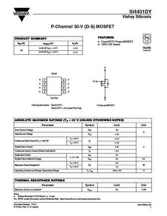
si4431cdy.pdf

New Product Si4431CDY Vishay Siliconix P-Channel 30-V (D-S) MOSFET FEATURES PRODUCT SUMMARY Halogen-free According to IEC 61249-2-21 VDS (V) RDS(on) ( ) ID (A)d Qg (Typ.) Definition 0.032 at VGS = - 10 V - 9.0 TrenchFET Power MOSFET - 30 13 nC 100 % Rg Tested 0.049 at VGS = - 4.5 V - 5.8 APPLICATIONS Load Switch Battery Switch SO-8 S S 1 8 D S
sq4431ey.pdf
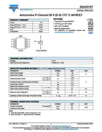
SQ4431EY www.vishay.com Vishay Siliconix Automotive P-Channel 30 V (D-S) 175 C MOSFET FEATURES PRODUCT SUMMARY TrenchFET Power MOSFET VDS (V) - 30 100 % Rg and UIS Tested RDS(on) ( ) at VGS = - 10 V 0.030 AEC-Q101 Qualifiedc RDS(on) ( ) at VGS = - 4.5 V 0.052 Material categorization ID (A) - 10.8 For definitions of compliance please see Configuration
sib431ed.pdf
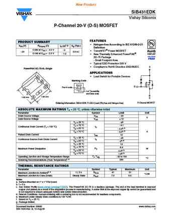
New Product SiB431EDK Vishay Siliconix P-Channel 20-V (D-S) MOSFET FEATURES PRODUCT SUMMARY Halogen-free According to IEC 61249-2-21 VDS (V) RDS(on) ( ) ID (A)f, g Qg (Typ.) Definition 0.080 at VGS = - 4.5 V - 9 TrenchFET Power MOSFET - 20 3.9 nC 0.149 at VGS = - 2.5 V - 1.2 New Thermally Enhanced PowerPAK SC-75 Package - Small Footprint Area Typical E
si4431cd.pdf
New Product Si4431CDY Vishay Siliconix P-Channel 30-V (D-S) MOSFET FEATURES PRODUCT SUMMARY Halogen-free According to IEC 61249-2-21 VDS (V) RDS(on) ( ) ID (A)d Qg (Typ.) Definition 0.032 at VGS = - 10 V - 9.0 TrenchFET Power MOSFET - 30 13 nC 100 % Rg Tested 0.049 at VGS = - 4.5 V - 5.8 APPLICATIONS Load Switch Battery Switch SO-8 S S 1 8 D S
sq1431eh.pdf
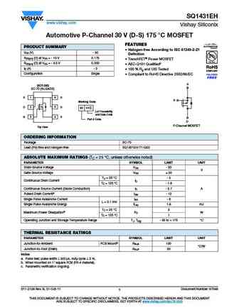
SQ1431EH www.vishay.com Vishay Siliconix Automotive P-Channel 30 V (D-S) 175 C MOSFET FEATURES PRODUCT SUMMARY Halogen-free According to IEC 61249-2-21 VDS (V) - 30 Definition RDS(on) ( ) at VGS = - 10 V 0.175 TrenchFET Power MOSFET RDS(on) ( ) at VGS = - 4.5 V 0.300 AEC-Q101 Qualifiedc ID (A) - 3 100 % Rg and UIS Tested Configuration Single Compliant
si4431bdy.pdf
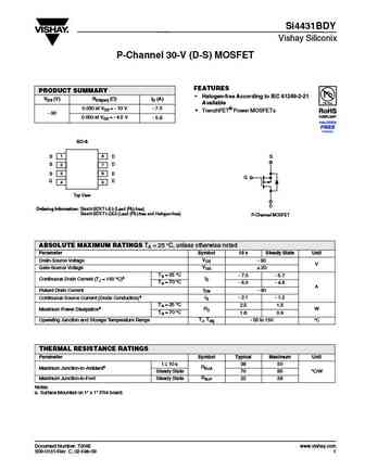
Si4431BDY Vishay Siliconix P-Channel 30-V (D-S) MOSFET FEATURES PRODUCT SUMMARY Halogen-free According to IEC 61249-2-21 VDS (V) RDS(on) ( )ID (A) Available 0.030 at VGS = - 10 V - 7.5 TrenchFET Power MOSFETs - 30 0.050 at VGS = - 4.5 V - 5.8 SO-8 S 1 8 D S S D 2 7 S 3 6 D G G D 4 5 Top View D Ordering Information Si4431BDY-T1-E3 (Lead (Pb)-free)
si7431dp.pdf
Si7431DP Vishay Siliconix P-Channel 200 V (D-S) MOSFET FEATURES PRODUCT SUMMARY Halogen-free According to IEC 61249-2-21 VDS (V) RDS(on) ( )ID (A) Qg (Typ.) Definition 0.174 at VGS = - 10 V - 3.8 TrenchFET Power MOSFETs - 200 88 0.180 at VGS = - 6 V - 3.6 Ultra-Low On-Resistance Critical for Application Low Thermal Resistance PowerPAK Package with Lo
2n6430 2n6431 2n6432 2n6433.pdf
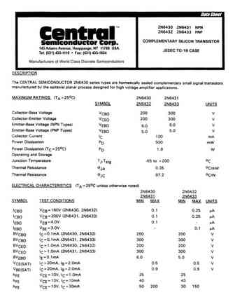
145 Adams Avenue, Hauppauge, NY 11788 USA Tel (631) 435-1110 Fax (631) 435-1824 TM Central Semiconductor Corp. 145 Adams Avenue Hauppauge, NY 11788 USA Tel (631) 435-1110 Fax (631) 435-1824 www.centralsemi.com
zvn4310a.pdf
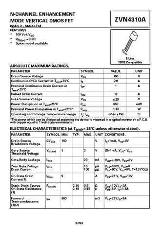
N-CHANNEL ENHANCEMENT ZVN4310A MODE VERTICAL DMOS FET ISSUE 2 MARCH 94 FEATURES . * 100 Volt VDS * RDS(on) = 0.5 * Spice model available D 1MHz G S E-Line TO92 Compatible ABSOLUTE MAXIMUM RATINGS. PARAMETER SYMBOL VALUE UNIT Drain-Source Voltage VDS 100 V ID=3A Continuous Drain Current at Tamb=25 C ID 0.9 A Practical Continuous Drain Current at IDP 1A Tamb=25 C P
zvn4310astoa zvn4310astob zvn4310astz.pdf

N-CHANNEL ENHANCEMENT ZVN4310A MODE VERTICAL DMOS FET ISSUE 2 MARCH 94 FEATURES . * 100 Volt VDS * RDS(on) = 0.5 * Spice model available D 1MHz G S E-Line TO92 Compatible ABSOLUTE MAXIMUM RATINGS. PARAMETER SYMBOL VALUE UNIT Drain-Source Voltage VDS 100 V ID=3A Continuous Drain Current at Tamb=25 C ID 0.9 A Practical Continuous Drain Current at IDP 1A Tamb=25 C P
zvn4310g.pdf
SOT223 N-CHANNEL ENHANCEMENT ZVN4310G MODE VERTICAL DMOS FET ISSUE 3 - FEBRUARY 1996 FEATURES * Very low RDS(ON) = .54 D APPLICATIONS * DC - DC Converters * Solenoids/Relay Drivers for Automotive S PARTMARKING DETAIL - ZVN4310 D G ABSOLUTE MAXIMUM RATINGS. 00 PARAMETER SYMBOL VALUE UNIT Drain-Source Voltage VDS 100 V Continuous Drain Current at Tamb=25 C ID 1.67 A Pulsed D
auirfs4310z.pdf
AUTOMOTIVE GRADE AUIRFS4310Z HEXFET Power MOSFET Features VDSS 100V Advanced Process Technology RDS(on) typ. 4.8m Ultra Low On-Resistance max. Dynamic dv/dt Rating 6.0m 175 C Operating Temperature ID (Silicon Limited) 127A Fast Switching ID (Package Limited) 120A Repetitive Avalanche Allowed up to Tjmax Lead-Free, RoHS
auirfs4310 auirfsl4310.pdf
AUIRFS4310 AUTOMOTIVE GRADE AUIRFSL4310 HEXFET Power MOSFET Features VDSS 100V Advanced Process Technology RDS(on) typ. 5.6m Ultra Low On-Resistance max. 7.0m 175 C Operating Temperature Fast Switching ID (Silicon Limited) 130A Repetitive Avalanche Allowed up to Tjmax ID (Package Limited) 75A Lead-Free, RoHS Compliant Au
ntmfs5h431nl.pdf
NTMFS5H431NL MOSFET Power, Single, N-Channel 40 V, 3.3 mW, 106 A Features Small Footprint (5x6 mm) for Compact Design www.onsemi.com Low RDS(on) to Minimize Conduction Losses Low QG and Capacitance to Minimize Driver Losses These Devices are Pb-Free and are RoHS Compliant V(BR)DSS RDS(ON) MAX ID MAX 3.3 mW @ 10 V 40 V MAXIMUM RATINGS (TJ = 25 C unless otherwise
fjaf4310.pdf

Is Now Part of To learn more about ON Semiconductor, please visit our website at www.onsemi.com Please note As part of the Fairchild Semiconductor integration, some of the Fairchild orderable part numbers will need to change in order to meet ON Semiconductor s system requirements. Since the ON Semiconductor product management systems do not have the ability to manage part nomenclatur
fds9431a.pdf
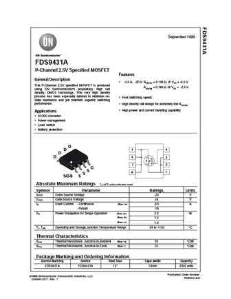
September 1999 FDS9431A P-Channel 2.5V Specified MOSFET Features General Description -3.5 A, -20 V. RDS(ON) = 0.130 @ VGS = -4.5 V This P-Channel 2.5V specified MOSFET is produced RDS(ON) = 0.180 @ VGS = -2.5 V. using ON Semiconductor's proprietary, high cell density, DMOS technology. This very high density process has been especially tailored to minimize on- Fast
fja4310.pdf

Is Now Part of To learn more about ON Semiconductor, please visit our website at www.onsemi.com Please note As part of the Fairchild Semiconductor integration, some of the Fairchild orderable part numbers will need to change in order to meet ON Semiconductor s system requirements. Since the ON Semiconductor product management systems do not have the ability to manage part nomenclatur
2sc5242 fja4313.pdf

Is Now Part of To learn more about ON Semiconductor, please visit our website at www.onsemi.com Please note As part of the Fairchild Semiconductor integration, some of the Fairchild orderable part numbers will need to change in order to meet ON Semiconductor s system requirements. Since the ON Semiconductor product management systems do not have the ability to manage part nomenclatur
fjl4315 2sc5200.pdf
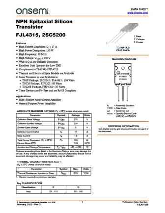
DATA SHEET www.onsemi.com NPN Epitaxial Silicon Transistor FJL4315, 2SC5200 1. Base 2. Collector 3. Emitter Features 1 High Current Capability IC = 17 A TO-264-3LD CASE 340CA High Power Dissipation 150 W High Frequency 30 MHz High Voltage VCEO = 250 V MARKING DIAGRAM Wide S.O.A. for Reliable Operation Excellent Gain Linearity for Low THD Comple
2sk2431.pdf
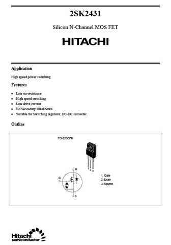
2SK2431 Silicon N-Channel MOS FET Application High speed power switching Features Low on-resistance High speed switching Low drive current No Secondary Breakdown Suitable for Switching regulator, DC-DC converter. Outline TO-220CFM 1 D 2 3 1. Gate G 2. Drain 3. Source S 2SK2431 Absolute Maximum Ratings (Ta = 25 C) Item Symbol Ratings Unit Drain to so
cv7431-o.pdf
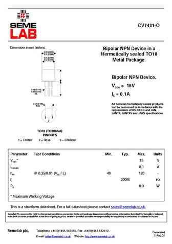
CV7431-O Dimensions in mm (inches). Bipolar NPN Device in a 5.84 (0.230) 5.31 (0.209) Hermetically sealed TO18 4.95 (0.195) 4.52 (0.178) Metal Package. Bipolar NPN Device. VCEO = 15V 0.48 (0.019) 0.41 (0.016) dia. IC = 0.1A 2.54 (0.100) All Semelab hermetically sealed products Nom. can be processed in accordance with the requirements of BS, CECC and JAN, JANTX, J
cv7431.pdf

CV7431 Dimensions in mm (inches). Bipolar NPN Device in a 5.84 (0.230) 5.31 (0.209) Hermetically sealed TO18 4.95 (0.195) 4.52 (0.178) Metal Package. Bipolar NPN Device. VCEO = 15V 0.48 (0.019) 0.41 (0.016) dia. IC = 0.1A 2.54 (0.100) All Semelab hermetically sealed products Nom. can be processed in accordance with the requirements of BS, CECC and JAN, JANTX, JAN
ssp7431p.pdf
SSP7431P -17A, -30V, RDS(ON) 13 m P-Channel Enhancement MOSFET Elektronische Bauelemente RoHS Compliant Product A suffix of -C specifies halogen & lead-free DESCRIPTION SOP-8PP These miniature surface mount MOSFETs utilize a high cell density trench process to provide low RDS(on) and to ensure minimal power loss and heat dissipation. FEATURES Low RDS(on) pro
tsm4431cs.pdf
TSM4431 30V P-Channel MOSFET SOP-8 Pin Definition PRODUCT SUMMARY 1. Source 2. Source VDS (V) RDS(on)(m ) ID (A) 3. Source 40 @ VGS = -10V -5.8 4. Gate -30 5, 6, 7, 8. Drain 70 @ VGS = -4.5V -4.5 Features Block Diagram Advance Trench Process Technology High Density Cell Design for Ultra Low On-resistance Application DC-DC Conversion A
2sd1431.pdf
NPN TRIPLE DIFFUSED 2SD1431 PLANAR SILICON TRANSISTOR COLOR TV HORIZONTAL OUTPUT APPLICATIONS(No Damper Diode) High Collector-Base Voltage(VCBO=1500V) 2-16D3A High Speed Switching ABSOLUTE MAXIMUM RATINGS (T =25oC) A Characteristic Symbol Rating Unit Collector-Base Voltage VCBO 1500 V Collector-Emitter Voltage VCEO 600 V Emitter-Base voltage VEBO 6 V Collector Current (DC) IC
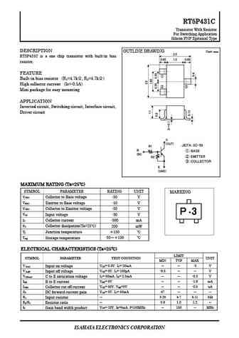
rt5n431c.pdf
RT5N431C Transistor With Resistor For Switching Application Silicon NPN Epitaxial Type DESCRIPTION OUTLINE DRAWING Unit mm 2.8 RT5N431C is a one chip transistor with built-in bias 0.65 1.5 0.65 resistor, PNP type is RT5P431C. FEATURE Built-in bias resistor R =4.7k , R =4.7k 1 2 High collector current Ic=0.5A Mini package for easy mounting
rt1n431c rt1n431m rt1n431s rt1n431u.pdf
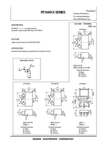
Transistor RT1N431X SERIES Transistor With Resistor For Switching Application Silicon NPN Epitaxial Type OUTLINE DRAWING DESCRIPTION UNIT mm RT1N431X is a one chip transistor RT1N431C with built-in bias resistor,PNP type is RT1P431X. 2.8 0.65 1.5 0.65 FEATURE Built-in bias resistor (R1=4.7k ,R2=4.7k ). APPLICATION Inverted circuit,swit
rt5p431c.pdf
RT5P431C Transistor With Resistor For Switching Application Silicon PNP Epitaxial Type DESCRIPTION OUTLINE DRAWING Unit mm 2.8 RT5P431C is a one chip transistor with built-in bias 0.65 1.5 0.65 resistor. FEATURE Built-in bias resistor R =4.7k , R =4.7k 1 2 High collector current Ic=-0.5A Mini package for easy mounting APPLICATION Inve
rt5p431s.pdf
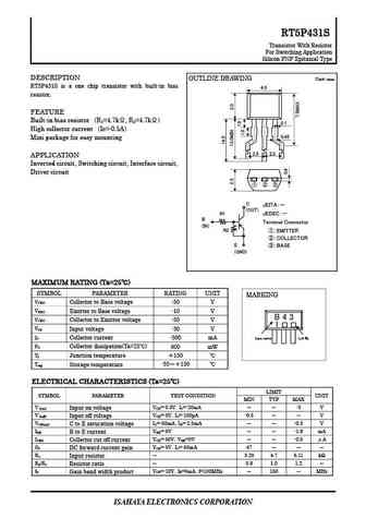
RT5P431S Transistor With Resistor For Switching Application Silicon PNP Epitaxial Type DESCRIPTION OUTLINE DRAWING Unit mm RT5P431S is a one chip transistor with built-in bias 4.0 resistor. FEATURE Built-in bias resistor R =4.7k , R =4.7k 1 2 0.1 High collector current Ic=-0.5A 0.45 Mini package for easy mounting 2.5 2.5 APPLICATION Inverted circ
rt1p431c rt1p431m rt1p431s.pdf
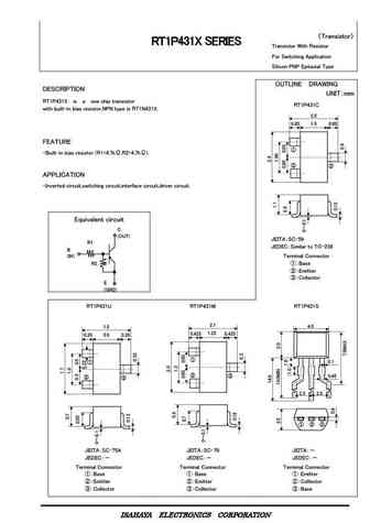
Transistor RT1P431X SERIES Transistor With Resistor For Switching Application Silicon PNP Epitaxial Type OUTLINE DRAWING DESCRIPTION UNIT mm RT1P431X is a one chip transistor RT1P431C with built-in bias resistor,NPN type is RT1N431X. 2.8 0.65 1.5 0.65 FEATURE Built-in bias resistor (R1=4.7k ,R2=4.7k ). APPLICATION Inverted circuit,s
sta431a.pdf
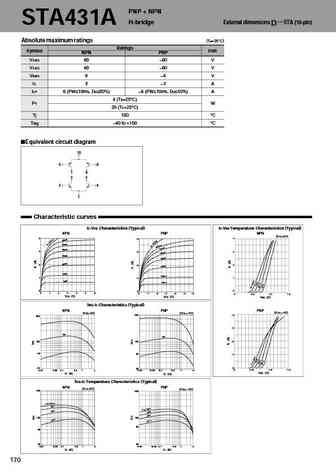
PNP + NPN H-bridge External dimensions STA (10-pin) STA431A D Absolute maximum ratings (Ta=25 C) Ratings Symbol Unit NPN PNP VCBO 60 60 V VCEO 60 60 V VEBO 6 6V IC 3 3A ICP 6 (PW 10ms, Du 50%) 6 (PW 10ms, Du 50%) A 4 (Ta=25 C) PT W 20 (Tc=25 C) Tj 150 C Tstg 40 to +150 C Equivalent circuit diagram 10 6 8 7 9 3 5 24 1 Charact
ced4311 ceu4311.pdf
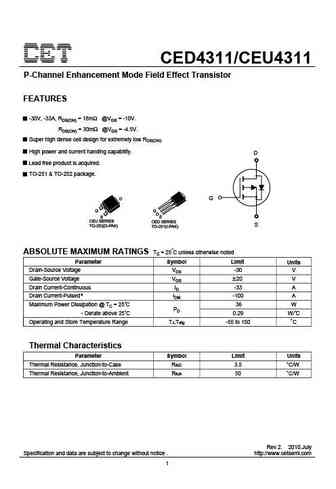
CED4311/CEU4311 P-Channel Enhancement Mode Field Effect Transistor FEATURES -30V, -33A, RDS(ON) = 18m @VGS = -10V. RDS(ON) = 30m @VGS = -4.5V. Super high dense cell design for extremely low RDS(ON). High power and current handing capability. D Lead free product is acquired. TO-251 & TO-252 package. D G G S CEU SERIES CED SERIES S TO-252(D-PAK) TO-251(I-PAK) ABSOLUTE MAX
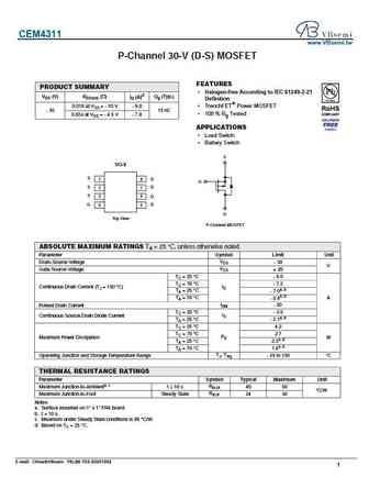
cem4311.pdf
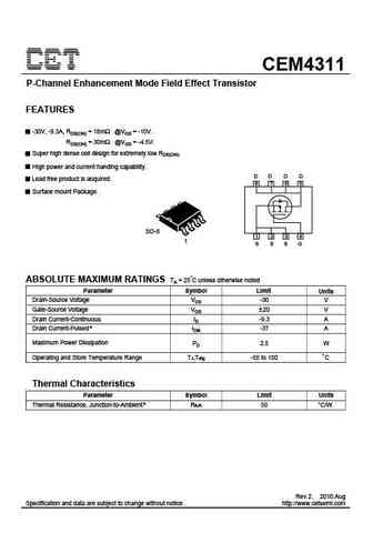
CEM4311 P-Channel Enhancement Mode Field Effect Transistor FEATURES -30V, -9.3A, RDS(ON) = 18m @VGS = -10V. RDS(ON) = 30m @VGS = -4.5V. Super high dense cell design for extremely low RDS(ON). High power and current handing capability. D D D D Lead free product is acquired. 8 7 6 5 Surface mount Package. SO-8 1 2 3 4 1 S S S G ABSOLUTE MAXIMUM RATINGS TA = 25 C unless othe
gm431.pdf
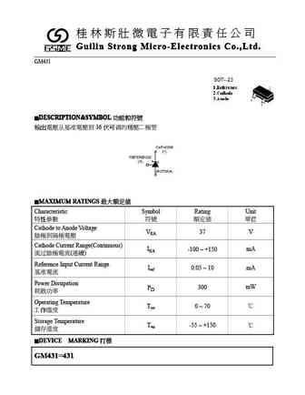
Guilin Strong Micro-Electronics Co.,Ltd. Guilin Strong Micro-Electronics Co.,Ltd. Guilin Strong Micro-Electronics Co.,Ltd. GM431 DESCRIPTION&SYMBOL DESCRIPTION&SYMBOL DESCRIPTION&SYMBOL 36 MAXIMUM RATINGS MAXIMUM RATINGS MAXIMUM RATINGS
wtk9431.pdf
WTK9431 Surface Mount P-Channel Enhancement Mode MOSFET DRAIN CURRENT P b Lead(Pb)-Free -3.5 AMPERES DRAIN SOURCE VOLTAGE Features -20 VOLTAGE * Super high dense * Cell design for low RDS(ON) * R
ao4314.pdf

AO4314 36V N-Channel MOSFET General Description Product Summary VDS 36V The AO4314 uses trench MOSFET technology that is uniquely optimized to provide the most efficient high ID (at VGS=10V) 20A frequency switching performance.Power losses are RDS(ON) (at VGS=10V)
ao4312.pdf
AO4312 36V N-Channel MOSFET General Description Product Summary VDS 36V The AO4312 uses trench MOSFET technology that is uniquely optimized to provide the most efficient high ID (at VGS=10V) 23A frequency switching performance.Power losses are RDS(ON) (at VGS=10V)
ao4310.pdf
AO4310 36V N-Channel MOSFET General Description Product Summary VDS 36V The AO4310 uses trench MOSFET technology that is uniquely optimized to provide the most efficient high ID (at VGS=10V) 27A frequency switching performance.Power losses are RDS(ON) (at VGS=10V)
aons74312.pdf
AONS74312 30V N-Channel MOSFET General Description Product Summary VDS 30V Trench Power MOSFET technology Very Low RDS(on) ID (at VGS=10V) 210A Low Gate Charge RDS(ON) (at VGS=10V)
ap9431gh-hf.pdf
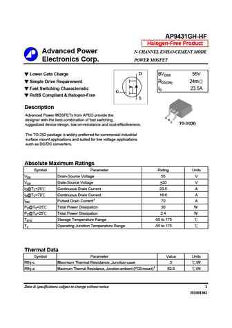
AP9431GH-HF Halogen-Free Product Advanced Power N-CHANNEL ENHANCEMENT MODE Electronics Corp. POWER MOSFET Lower Gate Charge D BVDSS 55V Simple Drive Requirement RDS(ON) 24m Fast Switching Characteristic ID 23.5A G RoHS Compliant & Halogen-Free S Description Advanced Power MOSFETs from APEC provide the G D designer with the best combination of fast switching,
am7431p.pdf
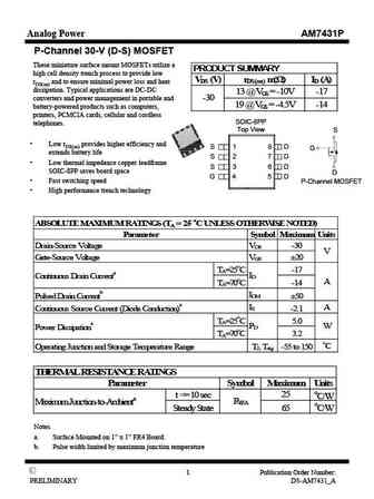
Analog Power AM7431P P-Channel 30-V (D-S) MOSFET These miniature surface mount MOSFETs utilize a PRODUCT SUMMARY high cell density trench process to provide low VDS (V) rDS(on) m( )ID (A) rDS(on) and to ensure minimal power loss and heat dissipation. Typical applications are DC-DC 13 @ VGS = -10V -17 converters and power management in portable and -30 19 @ VGS = -4.5V -14 batte
am4431p.pdf
Analog Power AM4431P P-Channel 30-V (D-S) MOSFET PRODUCT SUMMARY Key Features rDS(on) (m ) VDS (V) ID(A) Low r trench technology DS(on) 5 @ VGS = -10V -21 Low thermal impedance -30 7 @ VGS = -4.5V -17 Fast switching speed Typical Applications White LED boost converters Automotive Systems Industrial DC/DC Conversion Circuits ABSOLUTE MAXIMUM RA
amcc431p.pdf
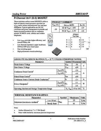
Analog Power AMCC431P P-Channel 30-V (D-S) MOSFET These miniature surface mount MOSFETs utilize a PRODUCT SUMMARY high cell density trench process to provide low VDS (V) rDS(on) m( ) ID (A) rDS(on) and to ensure minimal power loss and heat dissipation. Typical applications are DC-DC 60 @ VGS = -10V -5.9 converters and power management in portable and -30 90 @ VGS = -4.5V -4.8 b
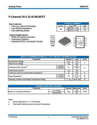
am3431p.pdf
Analog Power AM3431P P-Channel 30-V (D-S) MOSFET PRODUCT SUMMARY Key Features rDS(on) (m ) VDS (V) ID (A) Low r trench technology DS(on) 24 @ VGS = -10V -7.5 Low thermal impedance -30 36 @ VGS = -4.5V -6.1 Fast switching speed Typical Applications TSOP-6 Load Switches DC/DC Conversion Motor Drives ABSOLUTE MAXIMUM RATINGS (TA = 25 C UNLESS
am1431p.pdf
Analog Power AM1431P P-Channel 30-V (D-S) MOSFET These miniature surface mount MOSFETs utilize a high cell density trench process to provide low PRODUCT SUMMARY rDS(on) and to ensure minimal power loss and heat VDS (V) rDS(on) (OHM) ID (A) dissipation. Typical applications are DC-DC 0.112 @ VGS = -10V -3.1 converters and power management in portable and -30 battery-powered product
apm4315k.pdf
APM4315K P-Channel Enhancement Mode MOSFET Features Pin Description D D -30V/-11A, D D RDS(ON)= 11m (typ.) @ VGS=-10V RDS(ON)= 20m (typ.) @ VGS=-4.5V S S Super High Dense Cell Design S G Reliable and Rugged Lead Free and Green Devices Available Top View of SOP-8 (RoHS Compliant) ( 1, 2, 3 ) S S S Applications (4) G Power Management in Notebook Computer, Port
apm4317k.pdf
APM4317K P-Channel Enhancement Mode MOSFET Features Pin Description D D -30V/-9A, D D RDS(ON) = 16m (typ.) @ VGS = -10V RDS(ON) = 24m (typ.) @ VGS = -4.5V S S Super High Dense Cell Design S G Reliable and Rugged Lead Free and Green Devices Available Top View of SOP-8 (RoHS Compliant) ( 1, 2, 3 ) S S S Applications (4) G Power Management in Notebook Computer, P
apm4431k.pdf
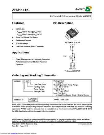
APM4431K P-Channel Enhancement Mode MOSFET Features Pin Description -30V/-5.3A , RDS(ON)=32m (typ.) @ VGS=-10V RDS(ON)=50m (typ.) @ VGS=-4.5V Super High Dense Cell Design Reliable and Rugged Top View of SOP - 8 SOP-8 Package (1, 2, 3) S S S Lead Free Available (RoHS Compliant) Applications (4)G Power Management in Notebook Computer, Portable Equipment and Batter
sm4310psk.pdf
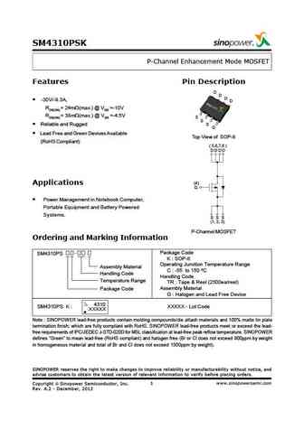
SM4310PSK P-Channel Enhancement Mode MOSFET Features Pin Description D D D -30V/-9.3A, D RDS(ON) = 24m (max.) @ VGS =-10V RDS(ON) = 38m (max.) @ VGS =-4.5V S S Reliable and Rugged S G Lead Free and Green Devices Available Top View of SOP-8 (RoHS Compliant) ( 5,6,7,8 ) D D D D (4) Applications G Power Management in Notebook Computer, Portable Equipment and Battery P
sm4311pskp.pdf
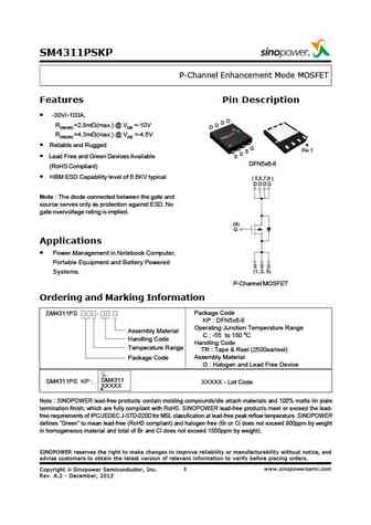
SM4311PSKP P-Channel Enhancement Mode MOSFET Features Pin Description -30V/-100A, D D RDS(ON) =2.8m (max.) @ VGS =-10V D D RDS(ON) =4.3m (max.) @ VGS =-4.5V Reliable and Rugged G Pin 1 S S Lead Free and Green Devices Available S DFN5x6-8 (RoHS Compliant) HBM ESD Capability level of 6.6KV typical ( 5,6,7,8 ) D D D D Note The diode connected between the gate and sour
ao4314.pdf
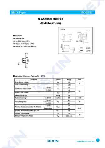
SMD Type MOSFET N-Channel MOSFET AO4314 (KO4314) SOP-8 Features VDS (V) = 36V 1.50 0.15 ID = 20 A (VGS = 10V) RDS(ON) 6m (VGS = 10V) RDS(ON) 8.5m (VGS = 4.5V) 1 Source 5 Drain 6 Drain 2 Source 7 Drain 3 Source 8 Drain 4 Gate D D G G S S Absolute Maximum Ratings Ta = 25 Parameter Symbol Rating Unit Drain-Source Voltage VDS 36
ao4312.pdf
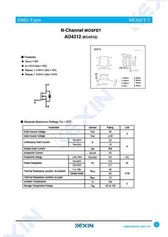
SMD Type MOSFET N-Channel MOSFET AO4312 (KO4312) SOP-8 Features VDS (V) = 36V ID = 23 A (VGS = 10V) 1.50 0.15 RDS(ON) 4.5m (VGS = 10V) RDS(ON) 6.2m (VGS = 4.5V) 1 Source 5 Drain 6 Drain 2 Source 7 Drain 3 Source D D 8 Drain 4 Gate G G S S Absolute Maximum Ratings Ta = 25 Parameter Symbol Rating Unit Drain-Source Voltage VDS 36
ao4310.pdf
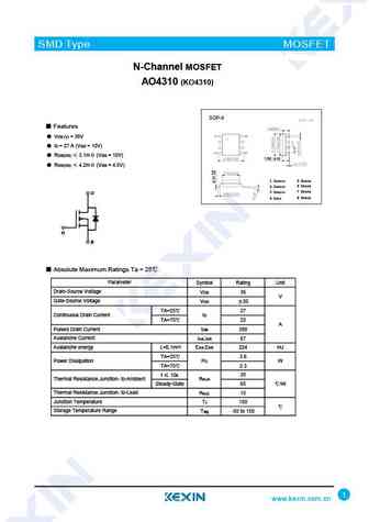
SMD Type MOSFET N-Channel MOSFET AO4310 (KO4310) SOP-8 Features VDS (V) = 36V ID = 27 A (VGS = 10V) RDS(ON) 3.1m (VGS = 10V) 1.50 0.15 RDS(ON) 4.2m (VGS = 4.5V) 1 Source 5 Drain 6 Drain 2 Source 7 Drain 3 Source D D 8 Drain 4 Gate G G S S Absolute Maximum Ratings Ta = 25 Parameter Symbol Rating Unit Drain-Source Voltage VDS 36
2sc4317.pdf
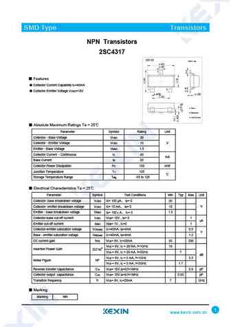
SMD Type Transistors NPN Transistors 2SC4317 SOT-23 Unit mm +0.1 2.9-0.1 +0.1 0.4 -0.1 3 Features Collector Current Capability IC=40mA 1 2 Collector Emitter Voltage VCEO=10V +0.05 0.95+0.1 -0.1 0.1 -0.01 1.9+0.1 -0.1 1.Base 2.Emitter 3.collector Absolute Maximum Ratings Ta = 25 Parameter Symbol Rating Unit Collector - Base Voltage VCBO 20 Collect
pja3431.pdf
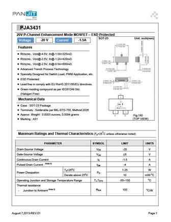
PPJA3431 20V P-Channel Enhancement Mode MOSFET ESD Protected SOT-23 Unit inch(mm) Voltage -20 V Current -1.5A Features RDS(ON) , VGS@-4.5V, ID@-1.5A
chm4311pagp.pdf
CHENMKO ENTERPRISE CO.,LTD CHM4311PAGP SURFACE MOUNT P-Channel Enhancement Mode Field Effect Transistor VOLTAGE 30 Volts CURRENT 33 Ampere APPLICATION * Servo motor control. * Power MOSFET gate drivers. * Other switching applications. D-PAK(TO-252) FEATURE * Small flat package. ( TO-252 ) * Super high density cell design for extremely low RDS(ON). .094 (2.40) * High power and
chm4431jgp.pdf

CHENMKO ENTERPRISE CO.,LTD CHM4431JGP SURFACE MOUNT P-Channel Enhancement Mode Field Effect Transistor VOLTAGE 30 Volts CURRENT 5.8 Ampere APPLICATION * Servo motor control. * Power MOSFET gate drivers. * Other switching applications. SO-8 FEATURE * Small flat package. (SO-8 ) ( ) * Super high dense cell design for extremely low RDS(ON). 4.06 0.160 ( ) 3.70 0.146 * High power
chm4311jgp.pdf
CHENMKO ENTERPRISE CO.,LTD CHM4311JGP SURFACE MOUNT P-Channel Enhancement Mode Field Effect Transistor VOLTAGE 30 Volts CURRENT 9.3 Ampere APPLICATION * Servo motor control. * Power MOSFET gate drivers. * Other switching applications. SO-8 FEATURE * Small flat package. (SO-8 ) ( ) * Super high dense cell design for extremely low RDS(ON). 4.06 0.160 ( ) 3.70 0.146 * High power
wej431.pdf
RoHS WEJ431 WEJ431 Adjustable Accurate Reference Source SOT-89 FEATURES The output voltage can be adjusted to 36V 1. REFERENCE Low dynamic output impedance, its typical value is 0.2 Trapping current capability is 1 to 100mA 1 2. ANODE The typical value of the equivalent temperature factor in the 2 whole temperature scope is 50 ppm/ 3 3. CATHODE The effec
hsm4313.pdf
HSM4313 Dual P-Ch 40V Fast Switching MOSFETs Description Product Summary The HSM4313 is the high cell density trenched P- V -40 V DS ch MOSFETs, which provide excellent RDSON and gate charge for most of the synchronous buck R 45 m DS(ON),max converter applications. I -6.5 A D The HSM4313 meet the RoHS and Green Product requirement, 100% EAS guaranteed with full fun
vba4317.pdf
VBA4317 www.VBsemi.com Dual P-Channel 30-V (D-S) MOSFET FEATURES PRODUCT SUMMARY Halogen-free VDS (V) RDS(on) ( ) ID (A)d, e Qg (Typ.) TrenchFET Power MOSFET 0.021 at VGS = - 10 V - 9.5 100 % UIS Tested RoHS - 30 15 nC COMPLIANT 0.028 at VGS = - 4.5 V - 8.0 APPLICATIONS Load Switches - Notebook PCs - Desktop PCs SO-8 S1 S2 - Game Stations S1 1 D1 8 G1
si4431cdy-t1-e3.pdf
SI4431CDY-T1-E3 www.VBsemi.tw P-Channel 30-V (D-S) MOSFET FEATURES PRODUCT SUMMARY Halogen-free According to IEC 61249-2-21 VDS (V) RDS(on) ( ) ID (A)d Qg (Typ.) Definition 0.018 at VGS = - 10 V - 9.0 TrenchFET Power MOSFET - 30 13 nC 100 % Rg Tested 0.024 at VGS = - 4.5 V - 7.8 APPLICATIONS Load Switch Battery Switch S SO-8 S 1 8 D G S D 2 7 S
irfl4310tr.pdf
IRFL4310TR www.VBsemi.tw N-Channel 30 V (D-S) MOSFET FEATURES PRODUCT SUMMARY TrenchFET Power MOSFET VDS (V) 30 AEC-Q101 Qualifiedc RDS(on) ( ) at VGS = 10 V 0.019 100 % Rg and UIS Tested RDS(on) ( ) at VGS = 4.5 V 0.021 ID (A) 7 Configuration Single D SOT-223 G D S D G S N-Channel MOSFET ABSOLUTE MAXIMUM RATINGS (TC = 25 C, unless otherwise noted) PA
vba4311.pdf
VBA4311 www.VBsemi.com Dual P-Channel 30-V (D-S) MOSFET FEATURES PRODUCT SUMMARY Halogen-free VDS (V) RDS(on) ( ) , ID (A)d, e Qg (Typ.) Typ. TrenchFET Power MOSFET 0.011 at VGS = - 10 V - 12 100 % UIS Tested RoHS - 30 15 nC COMPLIANT 0.013 at VGS = - 4.5 V - 10 APPLICATIONS Load Switches - Notebook PCs - Desktop PCs - Game Stations S1 S2 SO-8 S1 1 D1
cem4311.pdf
CEM4311 www.VBsemi.tw P-Channel 30-V (D-S) MOSFET FEATURES PRODUCT SUMMARY Halogen-free According to IEC 61249-2-21 VDS (V) RDS(on) ( ) ID (A)d Qg (Typ.) Definition 0.018 at VGS = - 10 V - 9.0 TrenchFET Power MOSFET - 30 13 nC 100 % Rg Tested 0.024 at VGS = - 4.5 V - 7.8 APPLICATIONS Load Switch Battery Switch S SO-8 S 1 8 D G S D 2 7 S 3 6 D G
hm4310.pdf
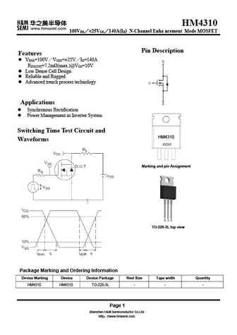
HM4310 100VDS 25VGS 140A(ID) N-Channel Enha ncement Mode MOSFET Pin Description Features VDSS=100V VGSS= 25V ID=140A RDS(ON)=7.2m (max.)@VGS=10V Low Dense Cell Design Reliable and Rugged Advanced trench process technology Applications Synchronous Rectification Power Management in Inverter System Switching Time Test Cir
2sk3431-z.pdf
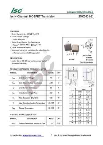
isc N-Channel MOSFET Transistor 2SK3431-Z FEATURES Drain Current I = 83A@ T =25 D C Drain Source Voltage V = 40V(Min) DSS Static Drain-Source On-Resistance R = 5.6m (Max) @ V = 10V DS(on) GS 100% avalanche tested Minimum Lot-to-Lot variations for robust device performance and reliable operation DESCRIPTION motor drive, DC-DC converter, power switch and solen
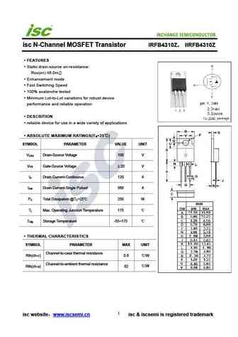
irfsl4310 .pdf
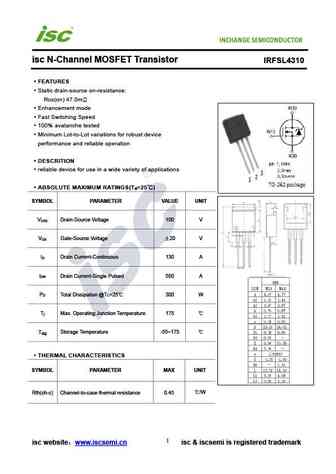
isc N-Channel MOSFET Transistor IRFSL4310 FEATURES Static drain-source on-resistance RDS(on) 7.0m Enhancement mode Fast Switching Speed 100% avalanche tested Minimum Lot-to-Lot variations for robust device performance and reliable operation DESCRITION reliable device for use in a wide variety of applications ABSOLUTE MAXIMUM RATINGS(T =25 ) a SYMBOL PARAM
2sb1431.pdf
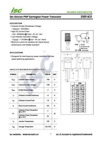
isc Silic on PNP Darlington Power Transistor 2SB1431 DESCRIPTION Collector-Emitter Breakdown Voltage- V = -100V(Min) (BR)CEO High DC Current Gain- h = 2000(Min)@ (V = -2V, I = -3A) FE CE C Low Collector Saturation Voltage- V = -1.5V(Max)@ (I = -3A, I = -3mA) CE(sat) C B Minimum Lot-to-Lot variations for robust device performance and reliable operation APPLICATIONS
2sk2431.pdf
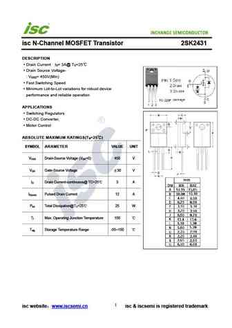
isc N-Channel MOSFET Transistor 2SK2431 DESCRIPTION Drain Current I = 3A@ T =25 D C Drain Source Voltage- V = 450V(Min) DSS Fast Switching Speed Minimum Lot-to-Lot variations for robust device performance and reliable operation APPLICATIONS Switching Regulators DC-DC Converter, Motor Control ABSOLUTE MAXIMUM RATINGS(T =25 ) a SYMBOL ARAMETER VALUE UNIT V Dr
irfb4310.pdf
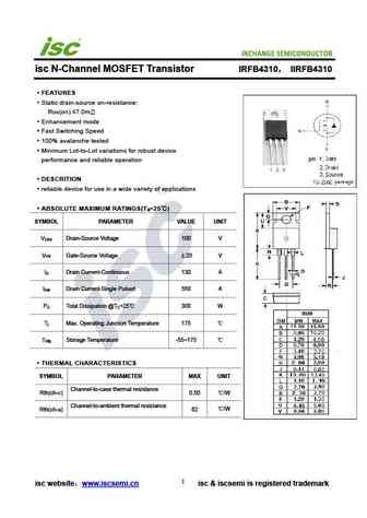
INCHANGE Semiconductor isc N-Channel MOSFET Transistor IRFB4310 IIRFB4310 FEATURES Static drain-source on-resistance RDS(on) 7.0m Enhancement mode Fast Switching Speed 100% avalanche tested Minimum Lot-to-Lot variations for robust device performance and reliable operation DESCRITION reliable device for use in a wide variety of applications ABSOLUTE MAXIMU
2sk3431.pdf
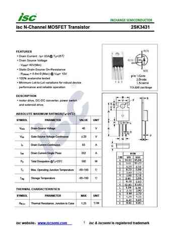
isc N-Channel MOSFET Transistor 2SK3431 FEATURES Drain Current I = 83A@ T =25 D C Drain Source Voltage V = 40V(Min) DSS Static Drain-Source On-Resistance R = 5.6m (Max) @ V = 10V DS(on) GS 100% avalanche tested Minimum Lot-to-Lot variations for robust device performance and reliable operation DESCRIPTION motor drive, DC-DC converter, power switch and solenoi
2sc1431.pdf
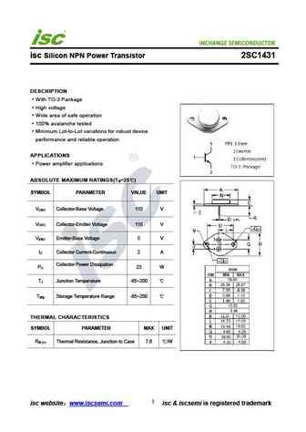
INCHANGE Semiconductor isc Silicon NPN Power Transistor 2SC1431 DESCRIPTION With TO-3 Package High voltage Wide area of safe operation 100% avalanche tested Minimum Lot-to-Lot variations for robust device performance and reliable operation APPLICATIONS Power amplifier applications ABSOLUTE MAXIMUM RATINGS(T =25 ) a SYMBOL PARAMETER VALUE UNIT V Collector-Base Voltage
irfb4310z.pdf
INCHANGE Semiconductor isc N-Channel MOSFET Transistor IRFB4310Z IIRFB4310Z FEATURES Static drain-source on-resistance RDS(on) 6.0m Enhancement mode Fast Switching Speed 100% avalanche tested Minimum Lot-to-Lot variations for robust device performance and reliable operation DESCRITION reliable device for use in a wide variety of applications ABSOLUTE MAXI
2sk3431-s.pdf
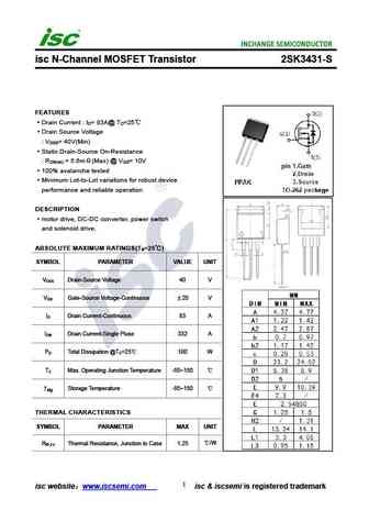
isc N-Channel MOSFET Transistor 2SK3431-S FEATURES Drain Current I = 83A@ T =25 D C Drain Source Voltage V = 40V(Min) DSS Static Drain-Source On-Resistance R = 5.6m (Max) @ V = 10V DS(on) GS 100% avalanche tested Minimum Lot-to-Lot variations for robust device performance and reliable operation DESCRIPTION motor drive, DC-DC converter, power switch and solen
2sd1431.pdf
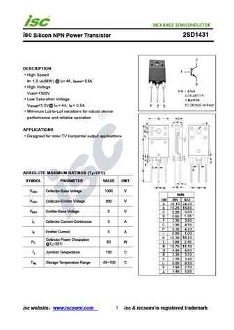
isc Silicon NPN Power Transistor 2SD1431 DESCRIPTION High Speed t = 1.0 us(MIN) @ I = 4A , I = 0.8A f C B(end) High Voltage V =1300V CBO Low Saturation Voltage V
irfs4310z.pdf
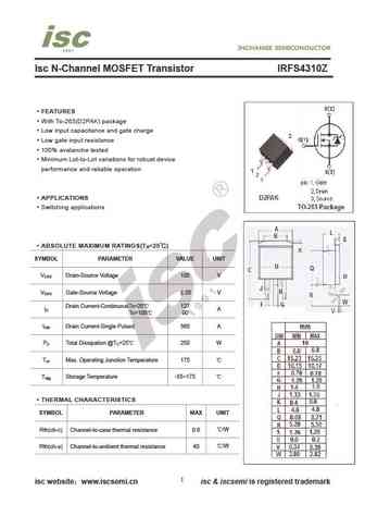
Isc N-Channel MOSFET Transistor IRFS4310Z FEATURES With To-263(D2PAK) package Low input capacitance and gate charge Low gate input resistance 100% avalanche tested Minimum Lot-to-Lot variations for robust device performance and reliable operation APPLICATIONS Switching applications ABSOLUTE MAXIMUM RATINGS(T =25 ) a SYMBOL PARAMETER VALUE UNIT V Drain-Source Vol
irfsl4310.pdf
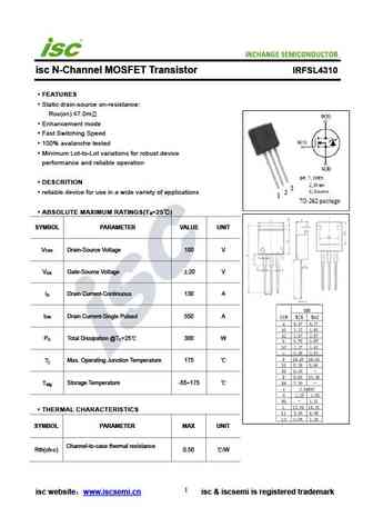
INCHANGE Semiconductor isc N-Channel MOSFET Transistor IRFSL4310 FEATURES Static drain-source on-resistance RDS(on) 7.0m Enhancement mode Fast Switching Speed 100% avalanche tested Minimum Lot-to-Lot variations for robust device performance and reliable operation DESCRITION reliable device for use in a wide variety of applications ABSOLUTE MAXIMUM RATINGS(T
mj431.pdf
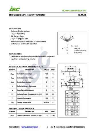
isc Silicon NPN Power Transistor MJ431 DESCRIPTION Collector-Emitter Voltage- V = 400V(Min) CEX DC Current Gain- h = 15-35@ I = 2.5A FE C Minimum Lot-to-Lot variations for robust device performance and reliable operation APPLICATIONS Designed for medium-to-high-voltage inverters, converters, regulators and switching circuits. ABSOLUTE MAXIMUM RATINGS(T =25 ) a SYMBO
irfp4310z.pdf
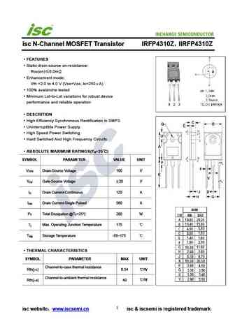
INCHANGE Semiconductor isc N-Channel MOSFET Transistor IRFP4310Z IIRFP4310Z FEATURES Static drain-source on-resistance RDS(on) 6.0m Enhancement mode Vth =2.0 to 4.0 V (VDS=VGS, ID=250 A) 100% avalanche tested Minimum Lot-to-Lot variations for robust device performance and reliable operation DESCRITION High Efficiency Synchronous Rectification in SMPS Unin
irfb4310zpbf.pdf
INCHANGE Semiconductor isc N-Channel MOSFET Transistor IRFB4310ZPBF FEATURES With TO-220 packaging High speed switching Easy to use 100% avalanche tested Minimum Lot-to-Lot variations for robust device performance and reliable operation APPLICATIONS Power supply DC-DC converters Motor control Switching applications ABSOLUTE MAXIMUM RATINGS(T =25 ) a SYM
2sc4313.pdf
INCHANGE Semiconductor isc Silicon NPN Power Transistor 2SC4313 DESCRIPTION Collector-Emitter Sustaining Voltage- VCEO(SUS)= 800V(Min) Fast Switching speed Minimum Lot-to-Lot variations for robust device performance and reliable operation APPLICATIONS Color TV horizontal output applications ABSOLUTE MAXIMUM RATINGS(T =25 ) a SYMBOL PARAMETER VALUE UNIT V Collector-Base
Другие транзисторы: 41501, 41502, 41503, 41504, 41505, 41506, 41508, 423, D880, 43104, 45190, 45191, 45192, 45193, 45194, 45195, 4NU72
Параметры биполярного транзистора и их взаимосвязь

Список транзисторов
Обновления
BJT: ZDT6705 | GA1L4Z | GA1A4M | SBT42 | 2SA200-Y | 2SA200-O | 2SD882-Q | 2SD882-P | 2SD882-E | 2SC945-L | 2SC945-H | 2SC4226-R23 | 2SC3357-F | 2SC3357-E | 2SC3356-R26 | 2SC3356-R24 | 2SC3356-R23 | 2SB772-Q | 2SB772-P | 2SB772-E | 2SA1015-L
Popular searches
ncep028n85 datasheet | sw50n06 | 2sa1232 | 2sc1940 | ftp08n06a | 2n3405 | 2n3567 | 2sc1226