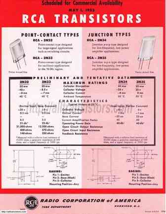
2N32 datasheet, аналоги, основные параметры
Наименование производителя: 2N32 📄📄
Тип материала: Ge
Полярность: PNP
Предельные значения
Максимальная рассеиваемая мощность (Pc): 0.05 W
Макcимально допустимое напряжение коллектор-база (Ucb): 40 V
Макcимально допустимое напряжение коллектор-эмиттер (Uce): 35 V
Макcимальный постоянный ток коллектора (Ic): 0.008 A
Предельная температура PN-перехода (Tj): 100 °C
Электрические характеристики
Граничная частота коэффициента передачи тока (ft): 0.9 MHz
Ёмкость коллекторного перехода (Cc): 45 pf
Статический коэффициент передачи тока (hFE): 22
Корпус транзистора: TO22
📄📄 Копировать
Аналоги (замена) для 2N32
- подборⓘ биполярного транзистора по параметрам
2N32 даташит
0.8. Size:88K central
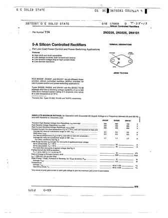
2n3250 2n3251.pdf 
145 Adams Avenue, Hauppauge, NY 11788 USA Tel (631) 435-1110 Fax (631) 435-1824
0.10. Size:11K semelab
2n3251csm.pdf 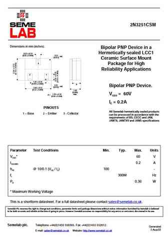
2N3251CSM Dimensions in mm (inches). Bipolar PNP Device in a 0.51 0.10 Hermetically sealed LCC1 (0.02 0.004) 0.31 rad. (0.012) Ceramic Surface Mount 3 Package for High Reliability Applications 21 1.91 0.10 (0.075 0.004) A 0.31 rad. Bipolar PNP Device. (0.012) 3.05 0.13 (0.12 0.005) 1.40 (0.055) 1.02 0.10 max. VCEO = 60V A = (0.04 0.004
0.11. Size:11K semelab
2n3244.pdf 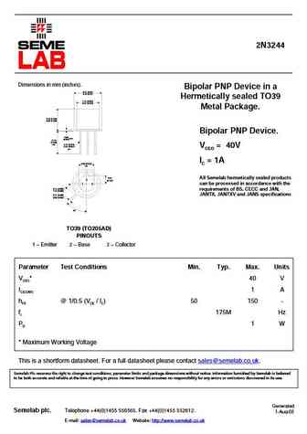
2N3244 Dimensions in mm (inches). Bipolar PNP Device in a 8.51 (0.34) 9.40 (0.37) Hermetically sealed TO39 7.75 (0.305) 8.51 (0.335) Metal Package. 6.10 (0.240) 6.60 (0.260) Bipolar PNP Device. 0.89 max. (0.035) 12.70 (0.500) min. 0.41 (0.016) 0.53 (0.021) VCEO = 40V dia. IC = 1A 5.08 (0.200) typ. 2.54 All Semelab hermetically sealed products 2 (0.100) 1 3
0.12. Size:11K semelab
2n3202.pdf 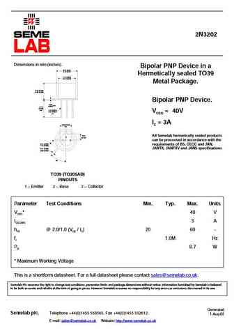
2N3202 Dimensions in mm (inches). Bipolar PNP Device in a 8.51 (0.34) 9.40 (0.37) Hermetically sealed TO39 7.75 (0.305) 8.51 (0.335) Metal Package. 6.10 (0.240) 6.60 (0.260) Bipolar PNP Device. 0.89 max. (0.035) 12.70 (0.500) min. 0.41 (0.016) 0.53 (0.021) VCEO = 40V dia. IC = 3A 5.08 (0.200) typ. 2.54 All Semelab hermetically sealed products 2 (0.100) 1 3
0.13. Size:24K semelab
2n3209x.pdf 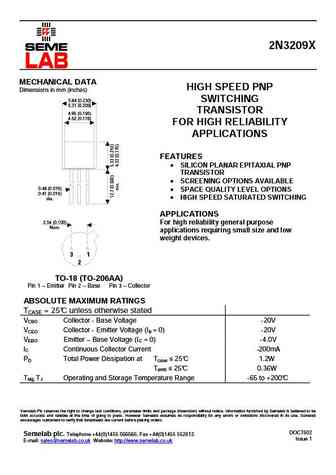
2N3209X MECHANICAL DATA HIGH SPEED PNP Dimensions in mm (inches) 5.84 (0.230) SWITCHING 5.31 (0.209) TRANSISTOR 4.95 (0.195) 4.52 (0.178) FOR HIGH RELIABILITY APPLICATIONS FEATURES SILICON PLANAR EPITAXIAL PNP TRANSISTOR SCREENING OPTIONS AVAILABLE 0.48 (0.019) SPACE QUALITY LEVEL OPTIONS 0.41 (0.016) HIGH SPEED SATURATED SWITCHING dia. APPLI
0.14. Size:25K semelab
2n3209xcsm.pdf 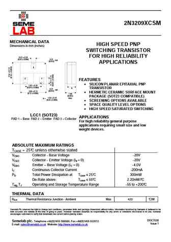
2N3209XCSM MECHANICAL DATA HIGH SPEED PNP Dimensions in mm (inches) SWITCHING TRANSISTOR FOR HIGH RELIABILITY 0.51 0.10 (0.02 0.004) 0.31 rad. (0.012) APPLICATIONS 3 2 1 FEATURES SILICON PLANAR EPITAXIAL PNP 1.91 0.10 (0.075 0.004) A TRANSISTOR 0.31 rad. (0.012) 3.05 0.13 HERMETIC CERAMIC SURFACE MOUNT (0.12 0.005) 1.40 (0.055) PA
0.15. Size:417K semelab
2n3251dcsm.pdf 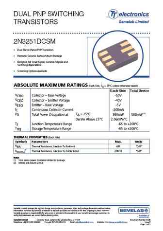
DUAL PNP SWITCHING TRANSISTORS 2N3251DCSM Dual Silicon Planer PNP Transistors Hermetic Ceramic Surface Mount Package Designed For Small Signal, General Purpose and Switching Applications Screening Options Available ABSOLUTE MAXIMUM RATINGS (Each Side, TA = 25 C unless otherwise stated) Each Side Total Device VCBO Collector Base Voltage -50V VCEO C
0.16. Size:183K bocasemi
2n3250 2n3251-a.pdf 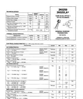
Boca Semiconductor Corp. BSC http //www.bocasemi.com http //www.bocasemi.com http //www.bocasemi.com http //www.bocasemi.com http //www.bocasemi.com
0.17. Size:208K cdil
2n3250 1.pdf 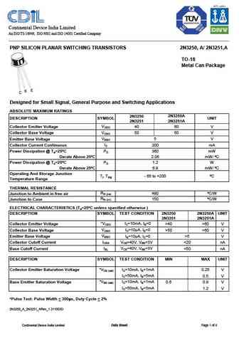
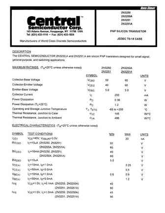
Continental Device India Limited An ISO/TS 16949, ISO 9001 and ISO 14001 Certified Company PNP SILICON PLANAR SWITCHING TRANSISTORS 2N3250, A/ 2N3251,A TO-18 Metal Can Package Designed for Small Signal, General Purpose and Switching Applications ABSOLUTE MAXIMUM RATINGS 2N3250 2N3250A DESCRIPTION SYMBOL UNIT 2N3251 2N3251A VCEO Collector Emitter Voltage 40 60 V VCBO Collector Bas
0.18. Size:129K microsemi
2n3250aub.pdf 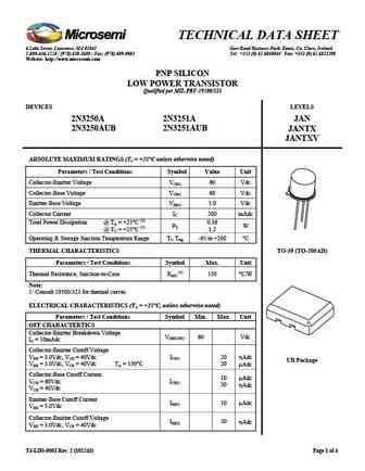
TECHNICAL DATA SHEET 6 Lake Street, Lawrence, MA 01841 Gort Road Business Park, Ennis, Co. Clare, Ireland. 1-800-446-1158 / (978) 620-2600 / Fax (978) 689-0803 Tel +353 (0) 65 6840044 Fax +353 (0) 65 6822298 Website http //www.microsemi.com PNP SILICON LOW POWER TRANSISTOR Qualified per MIL-PRF-19500/323 DEVICES LEVELS 2N3250A 2N3251A JAN 2N3250AUB 2N3251AUB JANTX JAN
0.19. Size:347K willsemi
wpt2n32.pdf 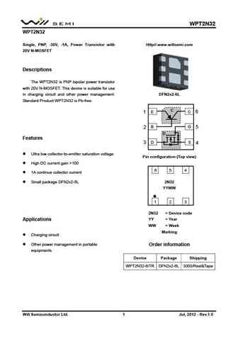
WPT2N32 WPT2N32 Single, PNP, -30V, -1A, Power Transistor with Http// www.willsemi.com 20V N-MOSFET Descriptions The WPT2N32 is PNP bipolar power transistor with 20V N-MOSFET. This device is suitable for use in charging circuit and other power management. DFN2x2-6L Standard Product WPT2N32 is Pb-free. C 6 1 E C B G 5 2 D Features D 3 S 4 Ultra low collec
0.20. Size:129K inchange semiconductor
2n3232.pdf 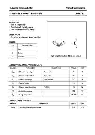
Inchange Semiconductor Product Specification Silicon NPN Power Transistors 2N3232 DESCRIPTION With TO-3 package Excellent safe operating area Low collector saturation voltage APPLICATIONS For audio amplifier and power switching PINNING PIN DESCRIPTION 1 Base 2 Emitter Fig.1 simplified outline (TO-3) and symbol 3 Collector ABSOLUTE MAXIMUM RATINGS(Ta=25 ) SYM
0.21. Size:129K inchange semiconductor
2n3233.pdf 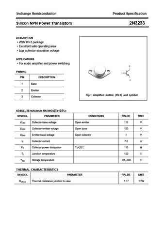
Inchange Semiconductor Product Specification Silicon NPN Power Transistors 2N3233 DESCRIPTION With TO-3 package Excellent safe operating area Low collector saturation voltage APPLICATIONS For audio amplifier and power switching PINNING PIN DESCRIPTION 1 Base 2 Emitter Fig.1 simplified outline (TO-3) and symbol 3 Collector ABSOLUTE MAXIMUM RATINGS(Ta=25 ) SYM
0.22. Size:171K inchange semiconductor
2n3238.pdf 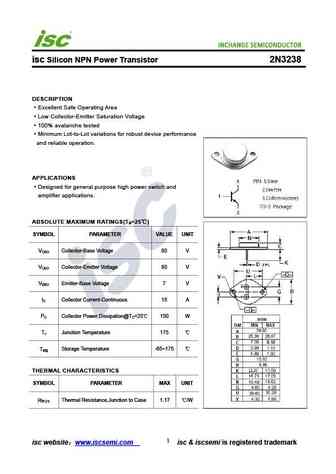
isc Silicon NPN Power Transistor 2N3238 DESCRIPTION Excellent Safe Operating Area Low Collector-Emitter Saturation Voltage 100% avalanche tested Minimum Lot-to-Lot variations for robust device performance and reliable operation. APPLICATIONS Designed for general purpose high power switch and amplifier applications. ABSOLUTE MAXIMUM RATINGS(T =25 ) a SYMBOL PARAMETER VALU
0.23. Size:170K inchange semiconductor
2n3239.pdf 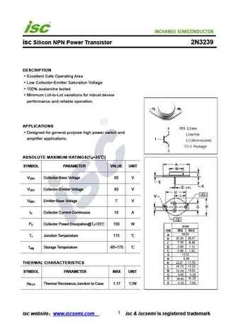
isc Silicon NPN Power Transistor 2N3239 DESCRIPTION Excellent Safe Operating Area Low Collector-Emitter Saturation Voltage 100% avalanche tested Minimum Lot-to-Lot variations for robust device performance and reliable operation. APPLICATIONS Designed for general purpose high power switch and amplifier applications. ABSOLUTE MAXIMUM RATINGS(T =25 ) a SYMBOL PARAMETER VALU
0.24. Size:170K inchange semiconductor
2n3226.pdf 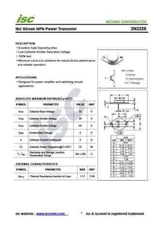
isc Silicon NPN Power Transistor 2N3226 DESCRIPTION Excellent Safe Operating Area Low Collector-Emitter Saturation Voltage 100% test Minimum Lot-to-Lot variations for robust device performance and reliable operation. APPLICATIONS Designed for power amplifier and switching circuits applications ABSOLUTE MAXIMUM RATINGS(T =25 ) a SYMBOL PARAMETER VALUE UNIT V Collector-Ba
0.25. Size:129K inchange semiconductor
2n3235.pdf 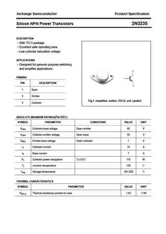
Inchange Semiconductor Product Specification Silicon NPN Power Transistors 2N3235 DESCRIPTION With TO-3 package Excellent safe operating area Low collector saturation voltage APPLICATIONS Designed for general purpose switching and amplifier applications. PINNING PIN DESCRIPTION 1 Base 2 Emitter Fig.1 simplified outline (TO-3) and symbol 3 Collector ABSOLUTE
0.26. Size:171K inchange semiconductor
2n3240.pdf 
isc Silicon NPN Power Transistor 2N3240 DESCRIPTION Excellent Safe Operating Area Low Collector-Emitter Saturation Voltage 100% avalanche tested Minimum Lot-to-Lot variations for robust device performance and reliable operation. APPLICATIONS Designed for general purpose high power switch and amplifier applications. ABSOLUTE MAXIMUM RATINGS(T =25 ) a SYMBOL PARAMETER VALU
0.27. Size:170K inchange semiconductor
2n3236.pdf 
isc Silicon NPN Power Transistor 2N3236 DESCRIPTION Excellent Safe Operating Area Low Collector-Emitter Saturation Voltage 100% avalanche tested Minimum Lot-to-Lot variations for robust device performance and reliable operation. APPLICATIONS Designed for general purpose high power switch and amplifier applications. ABSOLUTE MAXIMUM RATINGS(T =25 ) a SYMBOL PARAMETER VALU
0.28. Size:129K inchange semiconductor
2n3237.pdf 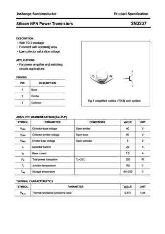
Inchange Semiconductor Product Specification Silicon NPN Power Transistors 2N3237 DESCRIPTION With TO-3 package Excellent safe operating area Low collector saturation voltage APPLICATIONS For power amplifier and switching circuits applications PINNING PIN DESCRIPTION 1 Base 2 Emitter Fig.1 simplified outline (TO-3) and symbol 3 Collector ABSOLUTE MAXIMUM RATIN
0.29. Size:129K inchange semiconductor
2n3234.pdf 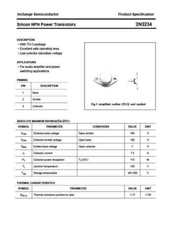
Inchange Semiconductor Product Specification Silicon NPN Power Transistors 2N3234 DESCRIPTION With TO-3 package Excellent safe operating area Low collector saturation voltage APPLICATIONS For audio amplifier and power switching applications PINNING PIN DESCRIPTION 1 Base 2 Emitter Fig.1 simplified outline (TO-3) and symbol 3 Collector ABSOLUTE MAXIMUM RATINGS(
Другие транзисторы: 2N3192, 2N3193, 2N3194, 2N3195, 2N3196, 2N3197, 2N3198, 2N3199, S9014, 2N320, 2N3200, 2N3201, 2N3202, 2N3203, 2N3204, 2N3205, 2N3206