1501 datasheet, аналоги, основные параметры
Наименование производителя: 1501 📄📄
Тип материала: Si
Полярность: NPN
Предельные значения
Максимальная рассеиваемая мощность (Pc): 0.6 W
Макcимально допустимое напряжение коллектор-база (Ucb): 30 V
Макcимально допустимое напряжение коллектор-эмиттер (Uce): 25 V
Макcимально допустимое напряжение эмиттер-база (Ueb): 4 V
Макcимальный постоянный ток коллектора (Ic): 0.05 A
Предельная температура PN-перехода (Tj): 150 °C
Электрические характеристики
Статический коэффициент передачи тока (hFE): 110
Корпус транзистора: TO92
📄📄 Копировать
Аналоги (замена) для 1501
- подборⓘ биполярного транзистора по параметрам
1501 даташит
0.2. Size:235K motorola
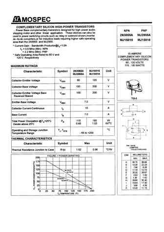
2n3055a mj2955a mj15015 mj15016.pdf 

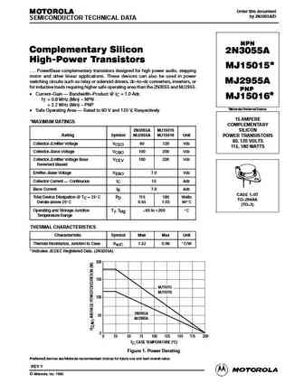
Order this document MOTOROLA by 2N3055A/D SEMICONDUCTOR TECHNICAL DATA NPN Complementary Silicon 2N3055A High-Power Transistors * MJ15015 . . . PowerBase complementary transistors designed for high power audio, stepping motor and other linear applications. These devices can also be used in power switching circuits such as relay or solenoid drivers, dc to dc converters, inverters
0.3. Size:129K motorola
mj15011r.pdf 

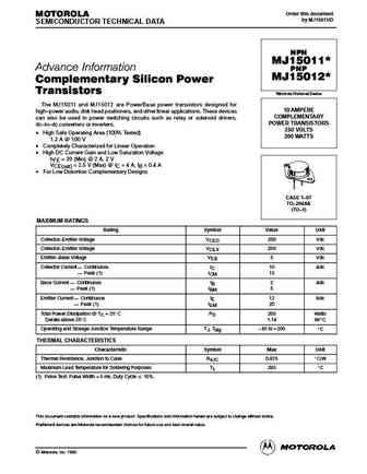
Order this document MOTOROLA by MJ15011/D SEMICONDUCTOR TECHNICAL DATA NPN MJ15011* Advance Information PNP MJ15012* Complementary Silicon Power Transistors *Motorola Preferred Device The MJ15011 and MJ15012 are PowerBase power transistors designed for 10 AMPERE high power audio, disk head positioners, and other linear applications. These devices COMPLEMENTARY can also be used
0.4. Size:135K motorola
mj15018r.pdf 

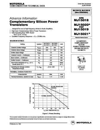
Order this document MOTOROLA by MJ15018/D SEMICONDUCTOR TECHNICAL DATA MJ15015, MJ15016 (See 2N3055A) NPN Advance Information MJ15018 Complementary Silicon Power MJ15020* Transistors PNP . . . designed for use as high frequency drivers in Audio Amplifiers. MJ15019 High Gain Complementary Silicon Power Transistors Safe Operating Area 100% Tested MJ15021* 50 V, 3.0 A, 1.
0.5. Size:146K toshiba
rn1501-1506.pdf 

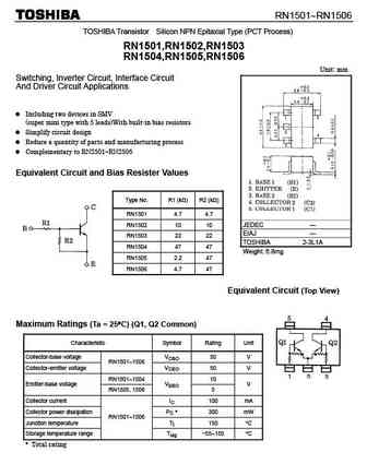
RN1501 RN1506 TOSHIBA Transistor Silicon NPN Epitaxial Type (PCT Process) RN1501,RN1502,RN1503 RN1504,RN1505,RN1506 Unit mm Switching, Inverter Circuit, Interface Circuit And Driver Circuit Applications Including two devices in SMV (super mini type with 5 leads)With built-in bias resistors Simplify circuit design Reduce a quantity of parts and manufacturing process
0.6. Size:92K nxp
pbls1501y-v.pdf 

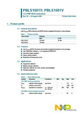
PBLS1501Y; PBLS1501V 15 V PNP BISS loadswitch Rev. 02 24 August 2009 Product data sheet 1. Product profile 1.1 General description Low VCEsat PNP transistor and NPN resistor-equipped transistor in one package. Table 1. Product overview Type number Package NXP JEITA PBLS1501Y SOT363 SC-88 PBLS1501V SOT666 - 1.2 Features Low VCEsat (BISS) transistor and resistor-equipped transist
0.7. Size:85K vishay
si1501dl.pdf 

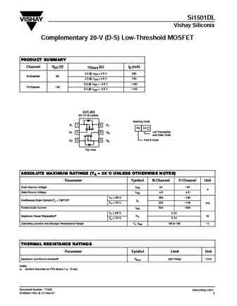
Si1501DL Vishay Siliconix Complementary 20-V (D-S) Low-Threshold MOSFET PRODUCT SUMMARY Channel VDS (V) rDS(on) (W) ID (mA) 2.0 @ VGS = 4.5 V 250 N-Channel 20 N-Channel 20 2.5 @ VGS = 2.5 V 150 3.8 @ VGS = -4.5 V -180 P Channel 20 P-Channel -20 5.0 @ VGS = -2.5 V -100 SOT-363 SC-70 (6-Leads) Marking Code S1 1 6 D1 RE XX Lot Traceability G1 2 5 G2 and Date Code 4 Part # Code
0.8. Size:356K infineon
ptfb211501e-f.pdf 

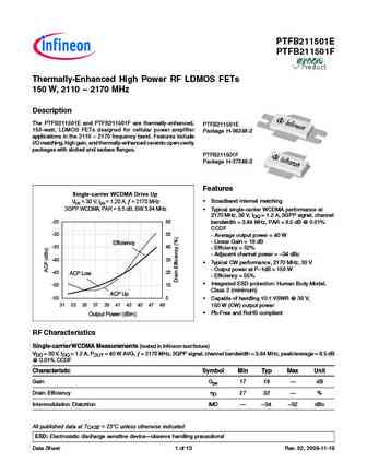
PTFB211501E PTFB211501F Thermally-Enhanced High Power RF LDMOS FETs 150 W, 2110 2170 MHz Description The PTFB211501E and PTFB211501F are thermally-enhanced, PTFB211501E 150-watt, LDMOS FETs designed for cellular power amplifier Package H-36248-2 applications in the 2110 2170 frequency band. Features include I/O matching, high gain, and thermally-enhanced ceramic open-cavity p
0.9. Size:289K infineon
ptfb191501e-f.pdf 

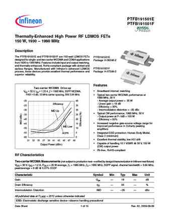
PTFB191501E PTFB191501F Confidential, Limited Internal Distribution Thermally-Enhanced High Power RF LDMOS FETs 150 W, 1930 1990 MHz Description The PTFB191501E and PTFB191501F are 150-watt LDMOS FETs PTFB191501E designed for single- and two-carrier WCDMA and CDMA applications Package H-36248-2 from 1930 to 1990 MHz. Features include input and output matching, and thermally-enhan
0.10. Size:430K infineon
ptfa041501e-f.pdf 

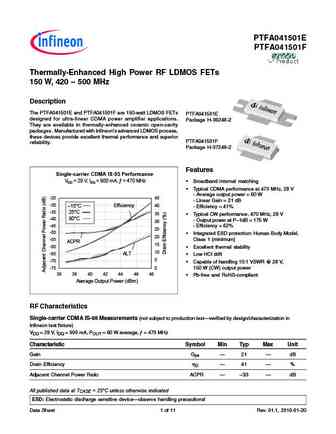
PTFA041501E PTFA041501F Confidential, Limited Internal Distribution Thermally-Enhanced High Power RF LDMOS FETs 150 W, 420 500 MHz Description The PTFA041501E and PTFA041501F are 150-watt LDMOS FETs PTFA041501E designed for ultra-linear CDMA power amplifier applications. Package H-36248-2 They are available in thermally-enhanced ceramic open-cavity packages . Manufactured with In
0.11. Size:89K onsemi
2n3055a mj15015 mj15016.pdf 

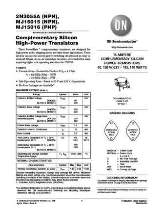
2N3055A (NPN), MJ15015 (NPN), MJ15016 (PNP) MJ15015 and MJ15016 are Preferred Devices Complementary Silicon High-Power Transistors http //onsemi.com These PowerBaset complementary transistors are designed for high power audio, stepping motor and other linear applications. These 15 AMPERE devices can also be used in power switching circuits such as relay or solenoid drivers, dc-to-dc
0.12. Size:181K onsemi
2n3055ag mj15015g mj15016g.pdf 

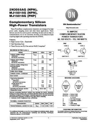
2N3055AG (NPN), MJ15015G (NPN), MJ15016G (PNP) Complementary Silicon High-Power Transistors http //onsemi.com These PowerBase complementary transistors are designed for high power audio, stepping motor and other linear applications. These 15 AMPERE devices can also be used in power switching circuits such as relay or COMPLEMENTARY SILICON solenoid drivers, dc-to-dc converters, invert
0.13. Size:61K onsemi
mj15011 mj15012.pdf 

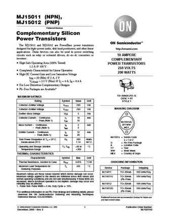
MJ15011 (NPN), MJ15012 (PNP) Preferred Devices Complementary Silicon Power Transistors The MJ15011 and MJ15012 are PowerBase power transistors designed for high-power audio, disk head positioners, and other linear http //onsemi.com applications. These devices can also be used in power switching circuits such as relay or solenoid drivers, dc-to-dc converters or 10 AMPERE inverters. CO
0.14. Size:89K onsemi
mj15016g.pdf 

2N3055A (NPN), MJ15015 (NPN), MJ15016 (PNP) MJ15015 and MJ15016 are Preferred Devices Complementary Silicon High-Power Transistors http //onsemi.com These PowerBaset complementary transistors are designed for high power audio, stepping motor and other linear applications. These 15 AMPERE devices can also be used in power switching circuits such as relay or solenoid drivers, dc-to-dc
0.15. Size:89K onsemi
mj15015g.pdf 

2N3055A (NPN), MJ15015 (NPN), MJ15016 (PNP) MJ15015 and MJ15016 are Preferred Devices Complementary Silicon High-Power Transistors http //onsemi.com These PowerBaset complementary transistors are designed for high power audio, stepping motor and other linear applications. These 15 AMPERE devices can also be used in power switching circuits such as relay or solenoid drivers, dc-to-dc
0.18. Size:658K alfa-mos
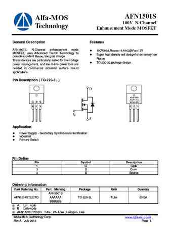
afn1501s.pdf 

AFN1501S Alfa-MOS 100V N-Channel Technology Enhancement Mode MOSFET General Description Features AFN1501S, N-Channel enhancement mode 100V/60A,RDS(ON)= 6.4m @VGS=10V MOSFET, uses Advanced Trench Technology to Super high density cell design for extremely low provide excellent RDS(ON), low gate charge. RDS (ON) These devices are particularly suited for low voltage TO-220-
0.19. Size:226K sino
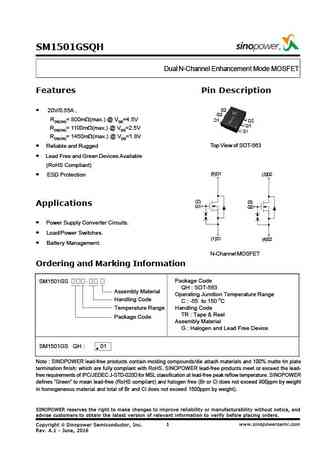
sm1501gsqh.pdf 

SM1501GSQH Dual N-Channel Enhancement Mode MOSFET Features Pin Description S2 20V/0.55A , G2 RDS(ON)= 800m (max.) @ VGS=4.5V D1 D2 G1 RDS(ON)= 1100m (max.) @ VGS=2.5V S1 RDS(ON)= 1450m (max.) @ VGS=1.8V Top View of SOT-563 Reliable and Rugged Lead Free and Green Devices Available (RoHS Compliant) (6)D1 (3)D2 ESD Protection (2) (5) Applications G1 G2 Power Suppl
0.20. Size:54K kexin
ki1501dl.pdf 

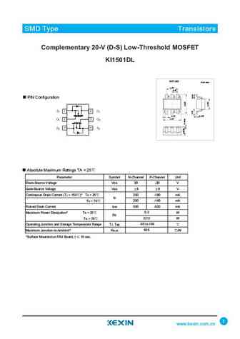
SMD Type IC SMD Type Transistors Complementary 20-V (D-S) Low-Threshold MOSFET KI1501DL SOT-363 Unit mm +0.1 1.3-0.1 0.65 PIN Configuration +0.1 +0.05 0.1-0.02 0.3-0.1 +0.1 2.1-0.1 Absolute Maximum Ratings TA = 25 Parameter Symbol N-Channel P-Channel Unit Drain-Source Voltage VDS 20 -20 V Gate-Source Voltage VGS 8 8 V Continuous Drain Current (TJ = 150 )* TA =25 250 -180 mA
0.21. Size:672K magnachip
mdd1501rh.pdf 

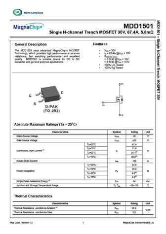
MDD1501 Single N-channel Trench MOSFET 30V, 67.4A, 5.6m General Description Features The MDD1501 uses advanced MagnaChip s MOSFET V = 30V DS Technology, which provides high performance in on-state I = 67.4A @V = 10V D GS resistance, fast switching performance and excellent R DS(ON) (MAX) quality. MDD1501 is suitable device for DC to DC
0.22. Size:704K magnachip
mdis1501th.pdf 

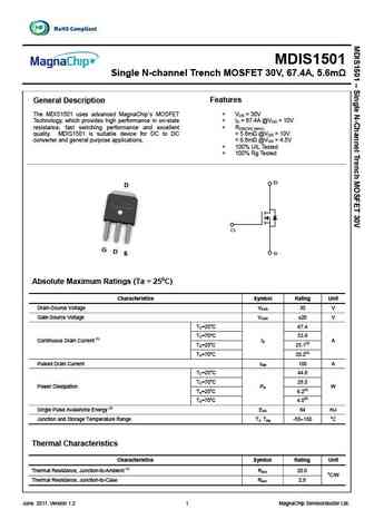
MDIS1501 Single N-channel Trench MOSFET 30V, 67.4A, 5.6m General Description Features The MDIS1501 uses advanced MagnaChip s MOSFET V = 30V DS Technology, which provides high performance in on-state I = 67.4A @V = 10V D GS resistance, fast switching performance and excellent R DS(ON) (MAX) quality. MDIS1501 is suitable device for DC to DC
0.23. Size:305K hgsemi
ms1501.pdf 

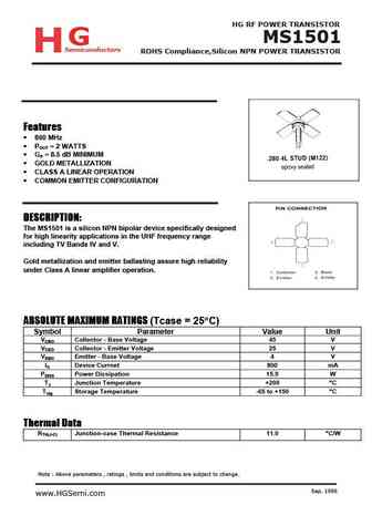
HG RF POWER TRANSISTOR MS1501 Semiconductors HG ROHS Compliance,Silicon NPN POWER TRANSISTOR Features Features 860 MHz POUT = 2 WATTS GP = 8.5 dB MINIMUM GOLD METALLIZATION CLASS A LINEAR OPERATION COMMON EMITTER CONFIGURATION DESCRIPTION DESCRIPTION The MS1501 is a silicon NPN bipolar device specifically designed for high linearity applications in the
0.24. Size:397K cn sino-ic
se150180g.pdf 

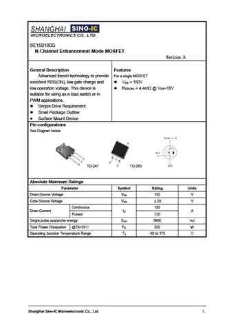
SE150180G N-Channel Enhancement-Mode MOSFET Revision A General Description Features For a single MOSFET Advanced trench technology to provide excellent RDS(ON), low gate charge and V = 150V DS low operation voltage. This device is R =4.4m @V =10V DS(ON) GS suitable for using as a load switch or in PWM applications. Simple Drive Requirement Small Package Outline
0.26. Size:339K cn sino-ic
se150180gts.pdf 

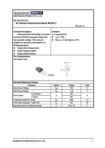
SE150180GTS N-Channel Enhancement-Mode MOSFET Revision A General Description Features For a single MOSFET Advanced trench technology to provide excellent RDS(ON), low gate charge and V = 150V DS low operation voltage. This device is R =4.8m @V =10V DS(ON) GS suitable for using as a load switch or in PWM applications. Simple Drive Requirement Small Package Outlin
0.27. Size:168K cn sptech
mj15016.pdf 

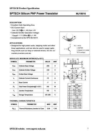
SPTECH Product Specification SPTECH Silicon PNP Power Transistor MJ15016 DESCRIPTION Excellent Safe Operating Area DC Current Gain- h = 20-70@I = -4A,V = -4V FE C CE Collector-Emitter Saturation Voltage- V )= -1.1 V(Max)@ I = -4A CE(sat C Complement to the NPN MJ15015 APPLICATIONS Designed for high power audio, stepping motor and other linear applications, and can als
0.28. Size:208K inchange semiconductor
mj15016.pdf 
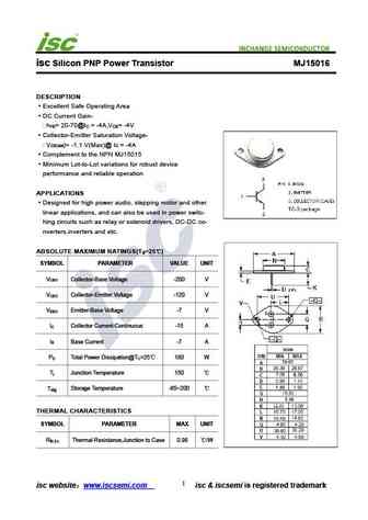
isc Silicon PNP Power Transistor MJ15016 DESCRIPTION Excellent Safe Operating Area DC Current Gain- h = 20-70@I = -4A,V = -4V FE C CE Collector-Emitter Saturation Voltage- V )= -1.1 V(Max)@ I = -4A CE(sat C Complement to the NPN MJ15015 Minimum Lot-to-Lot variations for robust device performance and reliable operation APPLICATIONS Designed for high power audio, step
0.29. Size:207K inchange semiconductor
mj15012.pdf 
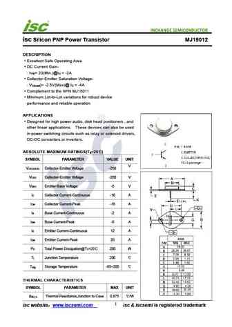
isc Silicon PNP Power Transistor MJ15012 DESCRIPTION Excellent Safe Operating Area DC Current Gain- h = 20(Min.)@I = -2A FE C Collector-Emitter Saturation Voltage- V )= -2.5V(Max)@ I = -4A CE(sat C Complement to the NPN MJ15011 Minimum Lot-to-Lot variations for robust device performance and reliable operation APPLICATIONS Designed for high power audio, disk head pos
0.30. Size:120K inchange semiconductor
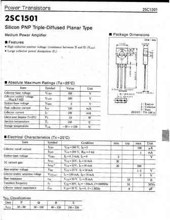
2sc1501.pdf 
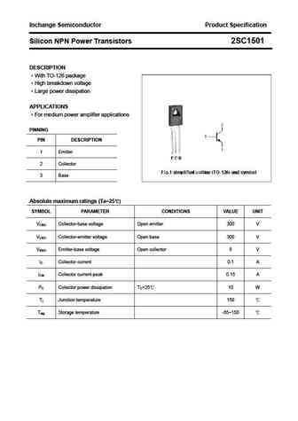
Inchange Semiconductor Product Specification Silicon NPN Power Transistors 2SC1501 DESCRIPTION With TO-126 package High breakdown voltage Large power dissipation APPLICATIONS For medium power amplifier applications PINNING PIN DESCRIPTION 1 Emitter 2 Collector 3 Base Absolute maximum ratings (Ta=25 ) SYMBOL PARAMETER CONDITIONS VALUE UNIT VCBO Collector-base
0.31. Size:207K inchange semiconductor
mj15011.pdf 
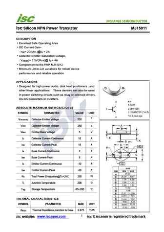
isc Silicon NPN Power Transistor MJ15011 DESCRIPTION Excellent Safe Operating Area DC Current Gain- h = 20(Min.)@I = 2A FE C Collector-Emitter Saturation Voltage- V )= 2.5V(Max)@ I = 4A CE(sat C Complement to the PNP MJ15012 Minimum Lot-to-Lot variations for robust device performance and reliable operation APPLICATIONS Designed for high power audio, disk head positi
0.32. Size:208K inchange semiconductor
mj15015.pdf 
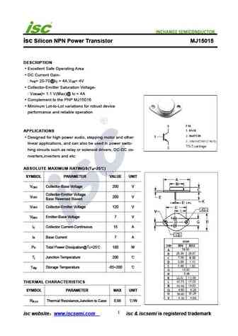
isc Silicon NPN Power Transistor MJ15015 DESCRIPTION Excellent Safe Operating Area DC Current Gain- h = 20-70@I = 4A,V = 4V FE C CE Collector-Emitter Saturation Voltage- V )= 1.1 V(Max)@ I = 4A CE(sat C Complement to the PNP MJ15016 Minimum Lot-to-Lot variations for robust device performance and reliable operation APPLICATIONS Designed for high power audio, stepping
Другие транзисторы: 121-713, 121-744, 121-746, 121-755, 121-792, 1401, 1402, 142T2, 2SC2073, 1502, 152NU70, 153NU70, 154NU70, 155NU70, 1601, 1602, 16029

