2N38 datasheet, аналоги, основные параметры
Наименование производителя: 2N38 📄📄
Тип материала: Ge
Полярность: PNP
Предельные значения
Максимальная рассеиваемая мощность (Pc): 0.05 W
Макcимально допустимое напряжение коллектор-база (Ucb): 20 V
Макcимальный постоянный ток коллектора (Ic): 0.008 A
Предельная температура PN-перехода (Tj): 80 °C
Электрические характеристики
Граничная частота коэффициента передачи тока (ft): 0.2 MHz
Статический коэффициент передачи тока (hFE): 10
Корпус транзистора: TO22
📄📄 Копировать
Аналоги (замена) для 2N38
- подборⓘ биполярного транзистора по параметрам
2N38 даташит
2n3866 2n4427.pdf
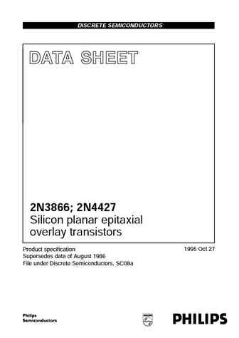
DISCRETE SEMICONDUCTORS DATA SHEET 2N3866; 2N4427 Silicon planar epitaxial overlay transistors 1995 Oct 27 Product specification Supersedes data of August 1986 File under Discrete Semiconductors, SC08a Philips Semiconductors Product specification Silicon planar epitaxial 2N3866; 2N4427 overlay transistors DESCRIPTION APPLICATIONS NPN overlay transistors in TO-39 metal packages wi
2n3810hr.pdf
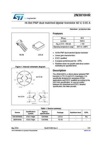
2N3810HR Hi-Rel PNP dual matched bipolar transistor 60 V, 0.05 A Datasheet - production data Features BVCEO 60 V IC (max) 0.05 A HFE at 10 V - 150 mA > 150 Operating temperature range -65 C to +200 C 1 2 3 4 6 5 Hi-Rel PNP dual matched bipolar transistor TO-78 LCC-6 Linear gain characteristics ESCC qualified European preferred part list - EPPL Radiatio
2n3820.pdf
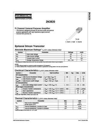
2N3820 P-Channel General Purpose Amplifier This device is designed primarily for low level audio and general purpose applications with high impedance signal sources. Sourced from process 89. TO-92 1 1. Drain 2. Gate 3. Source Epitaxial Silicon Transistor Absolute Maximum Ratings* TC=25 C unless otherwise noted Symbol Parameter Ratings Units VDG Drain-Gate Voltage -20 V VG
2n3859a.pdf
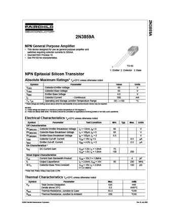
2N3859A NPN General Purpose Amplifier This device designed for use as general purpose amplifier and switches requiring collector currents to 300mA. Sourced from Process 10. See PN100 for characteristics. TO-92 1 1. Emitter 2. Collector 3. Base NPN Epitaxial Silicon Transistor Absolute Maximum Ratings* Ta=25 C unless otherwise noted Symbol Parameter Value Units VCEO C
2n3819.pdf
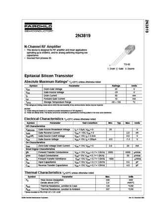
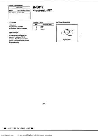
2N3819 N-Channel RF Amplifier This device is designed for RF amplifier and mixer applications operating up to 450MHz, and for analog switching requiring low capacitance. Sourced from process 50. TO-92 1 1. Drain 2. Gate 3. Source Epitaxial Silicon Transistor Absolute Maximum Ratings* TC=25 C unless otherwise noted Symbol Parameter Ratings Units VDG Drain-Gate Voltage 25
2n3819 2.pdf
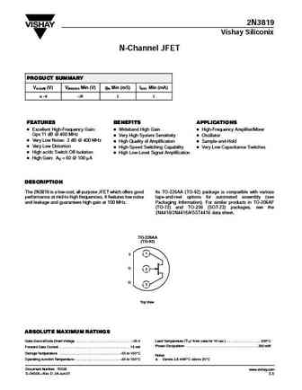
2N3819 Vishay Siliconix N-Channel JFET PRODUCT SUMMARY VGS(off) (V) V(BR)GSS Min (V) gfs Min (mS) IDSS Min (mA) v 8 25 2 2 FEATURES BENEFITS APPLICATIONS D Excellent High-Frequency Gain D Wideband High Gain D High-Frequency Amplifier/Mixer Gps 11 dB @ 400 MHz D Very High System Sensitivity D Oscillator D Very Low Noise 3 dB @ 400 MHz D High Quality of Amplification D Sample-a
2n2857 2n3839.pdf
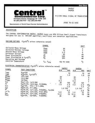
145 Adams Avenue, Hauppauge, NY 11788 USA Tel (631) 435-1110 Fax (631) 435-1824
2n3866 series.pdf
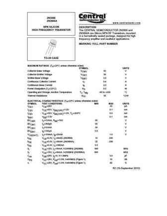
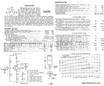
2N3866 2N3866A www.centralsemi.com NPN SILICON DESCRIPTION HIGH FREQUENCY TRANSISTOR The CENTRAL SEMICONDUCTOR 2N3866 and 2N3866A are Silicon NPN RF Transistors, mounted in a hermetically sealed package, designed for high frequency amplifier and oscillator applications. MARKING FULL PART NUMBER TO-39 CASE MAXIMUM RATINGS (TA=25 C unless otherwise noted) SYMBOL UNITS Collec
2n3821 2n3822 2n3824.pdf
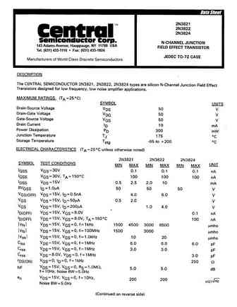
145 Adams Avenue, Hauppauge, NY 11788 USA Tel (631) 435-1110 Fax (631) 435-1824
2n3819.pdf
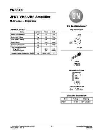
2N3819 JFET VHF/UHF Amplifier N Channel Depletion MAXIMUM RATINGS http //onsemi.com Rating Symbol Value Unit Drain Source Voltage VDS 25 Vdc 3 DRAIN Drain Gate Voltage VDG 25 Vdc Gate Source Voltage VGS 25 Vdc 2 Drain Current ID 100 mAdc GATE Forward Gate Current IG(f) 10 mAdc Total Device Dissipation PD 1 SOURCE @ TA = 25 C 350 mW Derate above 25 C 2.8 mW/ C St
2n3868s.pdf

The documentation and process conversion INCH-POUND measures necessary to comply with this revision MIL-PRF-19500/350M shall be completed by 30 November 2015. 31 August 2015 SUPERSEDING MIL-PRF-19500/350L 5 July 2010 PERFORMANCE SPECIFICATION SHEET * TRANSISTOR, PNP, SILICON, LOW POWER TYPES 2N3867, 2N3868, JAN, JANTX, JANTXV, JANS, JANHC, AND JANKC This specification is
2n3867u4.pdf

The documentation and process conversion INCH-POUND measures necessary to comply with this revision MIL-PRF-19500/350M shall be completed by 30 November 2015. 31 August 2015 SUPERSEDING MIL-PRF-19500/350L 5 July 2010 PERFORMANCE SPECIFICATION SHEET * TRANSISTOR, PNP, SILICON, LOW POWER TYPES 2N3867, 2N3868, JAN, JANTX, JANTXV, JANS, JANHC, AND JANKC This specification is
2n3867s.pdf
The documentation and process conversion INCH-POUND measures necessary to comply with this revision MIL-PRF-19500/350M shall be completed by 30 November 2015. 31 August 2015 SUPERSEDING MIL-PRF-19500/350L 5 July 2010 PERFORMANCE SPECIFICATION SHEET * TRANSISTOR, PNP, SILICON, LOW POWER TYPES 2N3867, 2N3868, JAN, JANTX, JANTXV, JANS, JANHC, AND JANKC This specification is
2n3868u4.pdf

The documentation and process conversion INCH-POUND measures necessary to comply with this revision MIL-PRF-19500/350M shall be completed by 30 November 2015. 31 August 2015 SUPERSEDING MIL-PRF-19500/350L 5 July 2010 PERFORMANCE SPECIFICATION SHEET * TRANSISTOR, PNP, SILICON, LOW POWER TYPES 2N3867, 2N3868, JAN, JANTX, JANTXV, JANS, JANHC, AND JANKC This specification is
2n3831.pdf
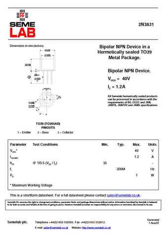
2N3831 Dimensions in mm (inches). Bipolar NPN Device in a 8.51 (0.34) 9.40 (0.37) Hermetically sealed TO39 7.75 (0.305) 8.51 (0.335) Metal Package. 6.10 (0.240) 6.60 (0.260) Bipolar NPN Device. 0.89 max. (0.035) 12.70 (0.500) min. 0.41 (0.016) 0.53 (0.021) VCEO = 40V dia. IC = 1.2A 5.08 (0.200) typ. 2.54 All Semelab hermetically sealed products 2 (0.100) 1
2n3804adcsm.pdf
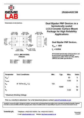
2N3804ADCSM Dimensions in mm (inches). Dual Bipolar PNP Devices in a hermetically sealed LCC2 Ceramic Surface Mount Package for High Reliability 1.40 0.15 2.29 0.20 1.65 0.13 (0.055 0.006) (0.09 0.008) (0.065 0.005) Applications 2 3 1 4 Dual Bipolar PNP Devices. A 0.23 6 5 rad. (0.009) V = 60V CEO 6.22 0.13 A = 1.27 0.13 I = 0.05A C (0
2n3879smd05.pdf
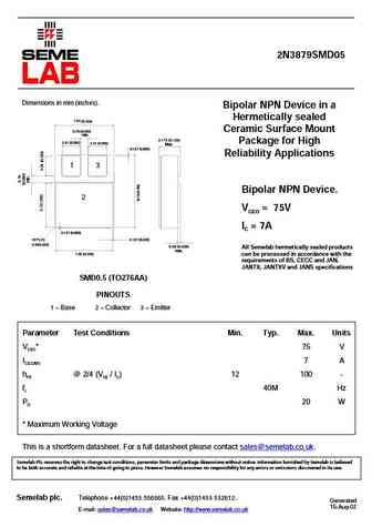
2N3879SMD05 Dimensions in mm (inches). Bipolar NPN Device in a Hermetically sealed 7.54 (0.296) 0.76 (0.030) Ceramic Surface Mount min. 3.175 (0.125) 2.41 (0.095) Package for High 2.41 (0.095) Max. 0.127 (0.005) Reliability Applications 1 3 Bipolar NPN Device. 2 VCEO = 75V IC = 7A 0.127 (0.005) 16 PLCS 0.127 (0.005) 0.50(0.020) 0.50 (0.020) All Semelab herm
2n3868smd05.pdf

2N3868SMD05 Dimensions in mm (inches). Bipolar PNP Device in a Hermetically sealed 7.54 (0.296) 0.76 (0.030) Ceramic Surface Mount min. 3.175 (0.125) 2.41 (0.095) Package for High 2.41 (0.095) Max. 0.127 (0.005) Reliability Applications 1 3 Bipolar PNP Device. 2 VCEO = 60V IC = 1A 0.127 (0.005) 16 PLCS 0.127 (0.005) 0.50(0.020) 0.50 (0.020) All Semelab herm
2n3868smd.pdf
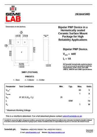
2N3868SMD Dimensions in mm (inches). Bipolar PNP Device in a Hermetically sealed 0.89 (0.035) min. Ceramic Surface Mount 3.70 (0.146) 3.70 (0.146) 3.60 (0.142) 3.41 (0.134) 3.41 (0.134) Max. Package for High Reliability Applications 1 3 Bipolar PNP Device. 2 VCEO = 60V IC = 1A 9.67 (0.381) All Semelab hermetically sealed products 9.38 (0.369) 0.50 (0.020) 0.26 (0
2n3879smd.pdf
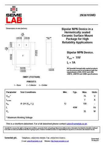
2N3879SMD Dimensions in mm (inches). Bipolar NPN Device in a Hermetically sealed 0.89 (0.035) min. Ceramic Surface Mount 3.70 (0.146) 3.70 (0.146) 3.60 (0.142) 3.41 (0.134) 3.41 (0.134) Max. Package for High Reliability Applications 1 3 Bipolar NPN Device. 2 VCEO = 75V IC = 7A 9.67 (0.381) All Semelab hermetically sealed products 9.38 (0.369) 0.50 (0.020) 0.26 (0
2n3828.pdf
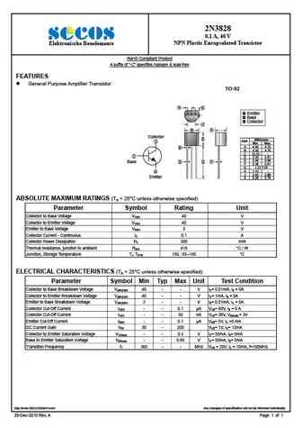
2N3828 0.1 A, 40 V NPN Plastic Encapsulated Transistor Elektronische Bauelemente RoHS Compliant Product A suffix of -C specifies halogen & lead-free FEATURES General Purpose Amplifier Transistor TO-92 G H Emitter Base Collector J A D Collector B Millimeter REF. Min. Max. A 4.40 4.70 K B 4.30 4.70 C 12.70 - D 3.30 3.81 E 0
2n3868.pdf
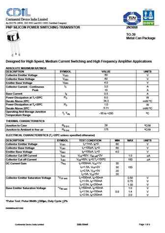
Continental Device India Limited An ISO/TS 16949, ISO 9001 and ISO 14001 Certified Company PNP SILICON POWER SWITCHING TRANSISTOR 2N3868 TO-39 Metal Can Package Designed for High Speed, Medium Current Switching and High Frequency Amplifier Applications ABSOLUTE MAXIMUM RATINGS DESCRIPTION SYMBOL VALUE UNITS VCEO Collector Emitter Voltage 60 V VCBO Collector Base Voltage 60 V VEBO
2n3867.pdf
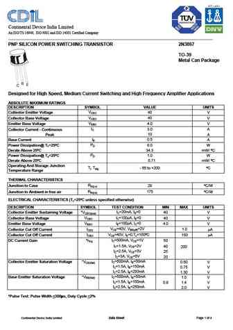
Continental Device India Limited An ISO/TS 16949, ISO 9001 and ISO 14001 Certified Company PNP SILICON POWER SWITCHING TRANSISTOR 2N3867 TO-39 Metal Can Package Designed for High Speed, Medium Current Switching and High Frequency Amplifier Applications ABSOLUTE MAXIMUM RATINGS DESCRIPTION SYMBOL VALUE UNITS VCEO Collector Emitter Voltage 40 V VCBO Collector Base Voltage 40 V VEBO
2n3821 2n3822.pdf
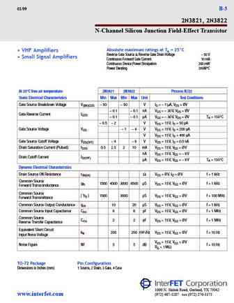
Databook.fxp 1/13/99 2 09 PM Page B-3 01/99 B-3 2N3821, 2N3822 N-Channel Silicon Junction Field-Effect Transistor Absolute maximum ratings at TA = 25 C VHF Amplifiers Reverse Gate Source & Reverse Gate Drain Voltage 50 V Small Signal Amplifiers Continuous Forward Gate Current 10 mA Continuous Device Power Dissipation 300 mW Power Derating 2mW/ C At 25 C free air temperat
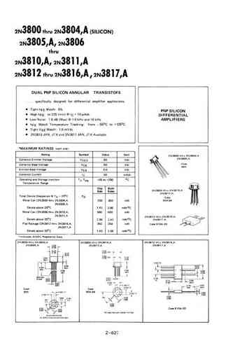
2n3810 2n3811.pdf
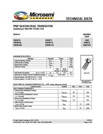
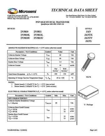
TECHNICAL DATA PNP SILICON DUAL TRANSISTOR Qualified per MIL-PRF-19500/336 Devices Qualified Level 2N3810 2N3811 JAN 2N3810L 2N3811L JANTX 2N3810U 2N3811U JANTXV MAXIMUM RATINGS Ratings Symbol Value Unit Collector-Emitter Voltage 60 Vdc VCEO Collector-Base Voltage 60 Vdc VCBO Emitter-Base Voltage 5.0 Vdc VEBO Collector Current 50 mAdc IC One Both Section 1
2n3866ub.pdf
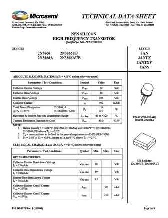
TECHNICAL DATA SHEET 6 Lake Street, Lawrence, MA 01841 Gort Road Business Park, Ennis, Co. Clare, Ireland 1-800-446-1158 / (978) 620-2600 / Fax (978) 689-0803 Tel +353 (0) 65 6840044 Fax +353 (0) 65 6822298 Website http //www.microsemi.com NPN SILICON HIGH-FREQUENCY TRANSISTOR Qualified per MIL-PRF-19500/398 DEVICES LEVELS 2N3866 2N3866UB JAN 2N3866A 2N3866AUB JANTX JANTX
2n3821 2n3822 2n3823.pdf
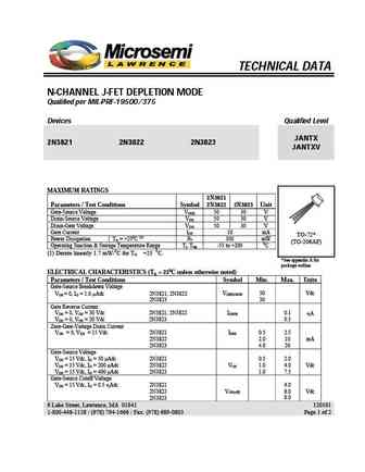
TECHNICAL DATA N-CHANNEL J-FET DEPLETION MODE Qualified per MIL-PRF-19500/375 Devices Qualified Level JANTX 2N3821 2N3822 2N3823 JANTXV MAXIMUM RATINGS 2N3821 Parameters / Test Conditions Symbol 2N3822 2N3823 Unit Gate-Source Voltage VGSR 50 30 V Drain-Source Voltage V 50 30 V DS Drain-Gate Voltage V 50 30 V DG Gate Current I 10 mA GF TO-72* Power Dissipatio
2n3868.pdf
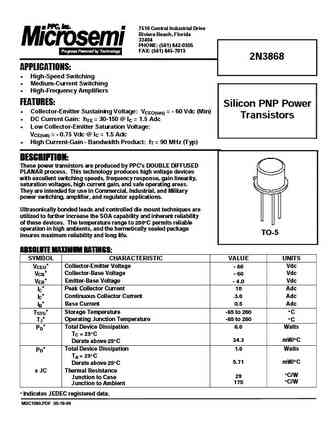
7516 Central Industrial Drive Riviera Beach, Florida 33404 PHONE (561) 842-0305 FAX (561) 845-7813 2N3868 APPLICATIONS High-Speed Switching Medium-Current Switching High-Frequency Amplifiers FEATURES Silicon PNP Power Collector-Emitter Sustaining Voltage VCEO(sus) = - 60 Vdc (Min) Transistors DC Current Gain hFE = 30-150 @ IC = 1.5 Adc Low Collector-
2n3810u.pdf

TECHNICAL DATA SHEET 6 Lake Street, Lawrence, MA 01841 6 Lake Street, Lawrence, MA 01841 Gort Road Business Park, Ennis, Co. Clare, Ireland 1-800-446-1158 / (978) 620-2600 / Fax (978) 689-0803 Tel +353 (0) 65 6840044 Fax +353 (0) 65 6822298 Website http //www.microsemi.com PNP SILICON DUAL TRANSISTOR Qualified per MIL-PRF-19500 /336 DEVICES LEVELS 2N3810 2N3811 JAN 2N3810L
2n3811l.pdf

TECHNICAL DATA SHEET 6 Lake Street, Lawrence, MA 01841 6 Lake Street, Lawrence, MA 01841 Gort Road Business Park, Ennis, Co. Clare, Ireland 1-800-446-1158 / (978) 620-2600 / Fax (978) 689-0803 Tel +353 (0) 65 6840044 Fax +353 (0) 65 6822298 Website http //www.microsemi.com PNP SILICON DUAL TRANSISTOR Qualified per MIL-PRF-19500 /336 DEVICES LEVELS 2N3810 2N3811 JAN 2N3810L
2n3810l.pdf
TECHNICAL DATA SHEET 6 Lake Street, Lawrence, MA 01841 6 Lake Street, Lawrence, MA 01841 Gort Road Business Park, Ennis, Co. Clare, Ireland 1-800-446-1158 / (978) 620-2600 / Fax (978) 689-0803 Tel +353 (0) 65 6840044 Fax +353 (0) 65 6822298 Website http //www.microsemi.com PNP SILICON DUAL TRANSISTOR Qualified per MIL-PRF-19500 /336 DEVICES LEVELS 2N3810 2N3811 JAN 2N3810L
2n3866.pdf
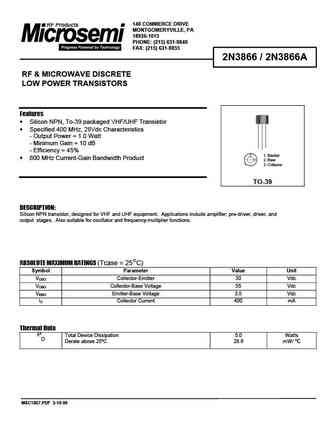
140 COMMERCE DRIVE MONTGOMERYVILLE, PA 18936-1013 PHONE (215) 631-9840 FAX (215) 631-9855 2N3866 / 2N3866A RF & MICROWAVE DISCRETE LOW POWER TRANSISTORS Features Silicon NPN, To-39 packaged VHF/UHF Transistor Specified 400 MHz, 28Vdc Characteristics - Output Power = 1.0 Watt - Minimum Gain = 10 dB - Efficiency = 45% 1. Emitter 800 MHz Current-Gain Bandwidth Produ
2n3838 2n4854.pdf
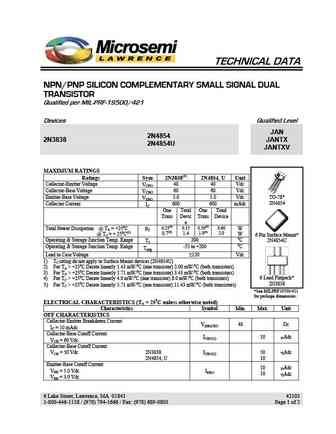
TECHNICAL DATA NPN/PNP SILICON COMPLEMENTARY SMALL SIGNAL DUAL TRANSISTOR Qualified per MIL-PRF-19500/421 Devices Qualified Level JAN 2N4854 2N3838 JANTX 2N4854U JANTXV MAXIMUM RATINGS Ratings Sym 2N3838(2) 2N4854, U Unit Collector-Emitter Voltage 40 40 Vdc VCEO Collector-Base Voltage 60 60 Vdc VCBO Emitter-Base Voltage 5.0 5.0 Vdc TO-78* VEBO 2N4854 Collector
2n3846 2n3847.pdf
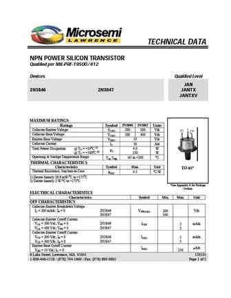
TECHNICAL DATA NPN POWER SILICON TRANSISTOR Qualified per MIL-PRF-19500/412 Devices Qualified Level JAN 2N3846 2N3847 JANTX JANTXV MAXIMUM RATINGS Ratings Symbol 2N3846 2N3847 Units Collector-Emitter Voltage 200 300 Vdc VCEO Collector-Base Voltage 300 400 Vdc VCBO Emitter-Base Voltage 10 Vdc VEBO Collector Current 20 Adc IC Total Power Dissipation @ T = +250C (
2n3867.pdf

7516 Central Industrial Drive Riviera Beach, Florida 33404 PHONE (561) 842-0305 FAX (561) 845-7813 2N3867 APPLICATIONS High-Speed Switching Medium-Current Switching High-Frequency Amplifiers FEATURES Silicon PNP Power Collector-Emitter Sustaining Voltage VCEO(sus) = - 40 Vdc (Min) Transistors DC Current Gain hFE = 40-200 @ IC = 1.5 Adc Low Collector-
2n3811u.pdf

TECHNICAL DATA SHEET 6 Lake Street, Lawrence, MA 01841 6 Lake Street, Lawrence, MA 01841 Gort Road Business Park, Ennis, Co. Clare, Ireland 1-800-446-1158 / (978) 620-2600 / Fax (978) 689-0803 Tel +353 (0) 65 6840044 Fax +353 (0) 65 6822298 Website http //www.microsemi.com PNP SILICON DUAL TRANSISTOR Qualified per MIL-PRF-19500 /336 DEVICES LEVELS 2N3810 2N3811 JAN 2N3810L
3da3866 2n3866.pdf
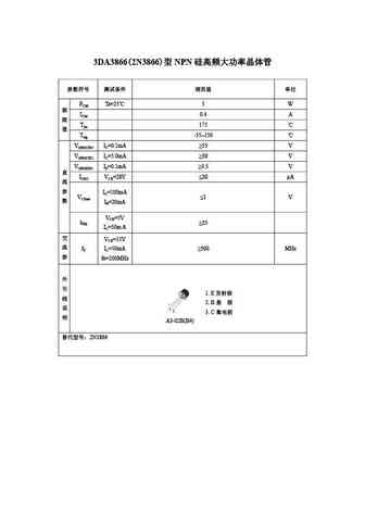
3DA3866(2N3866) NPN PCM Ta=25 5 W ICM 0.4 A Tjm 175 Tstg -55 150 V(BR)CBO IC=0.1mA 55 V V(BR)CEO IC=5.0mA 30 V V(BR)EBO IE=0.1mA 3.5 V ICEO VCE=28V 20 A IC=100mA VCEsat 1 V IB=20mA VCE=5V hFE 25 IC=50m A VCE=15V
2n3711 2n3721 2n3827 2n3858 2n3858a 2n3859 2n3859a 2n3860 2n3877 2n3877a 2n3900 2n3900a 2n3901 2n3903 2n3904 2n3905.pdf
2n3865.pdf

isc Silicon NPN Power Transistor 2N3865 DESCRIPTION Excellent Safe Operating Area Low Collector-Emitter Saturation Voltage 100% avalanche tested Minimum Lot-to-Lot variations for robust device performance and reliable operation. APPLICATIONS Designed for medium-speed switching and amplifier applications. ABSOLUTE MAXIMUM RATINGS(T =25 ) a SYMBOL PARAMETER VALUE UNIT V C
2n3878.pdf
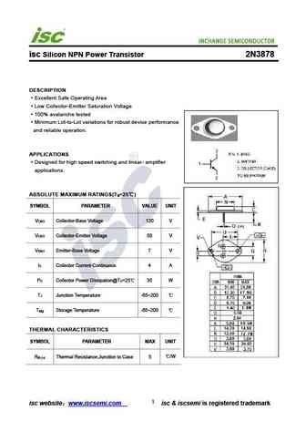
isc Silicon NPN Power Transistor 2N3878 DESCRIPTION Excellent Safe Operating Area Low Collector-Emitter Saturation Voltage 100% avalanche tested Minimum Lot-to-Lot variations for robust device performance and reliable operation. APPLICATIONS Designed for high speed switching and linear- amplifier applications. ABSOLUTE MAXIMUM RATINGS(T =25 ) a SYMBOL PARAMETER VALUE UNI
2n3879.pdf
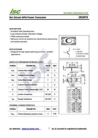
isc Silicon NPN Power Transistor 2N3879 DESCRIPTION Excellent Safe Operating Area Low Collector-Emitter Saturation Voltage 100% avalanche tested Minimum Lot-to-Lot variations for robust device performance and reliable operation. APPLICATIONS Designed for high speed switching and linear- amplifier applications. ABSOLUTE MAXIMUM RATINGS(T =25 ) a SYMBOL PARAMETER VALUE UNI
2n3863.pdf
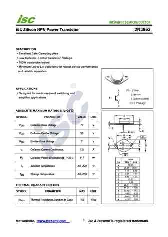
isc Silicon NPN Power Transistor 2N3863 DESCRIPTION Excellent Safe Operating Area Low Collector-Emitter Saturation Voltage 100% avalanche tested Minimum Lot-to-Lot variations for robust device performance and reliable operation. APPLICATIONS Designed for medium-speed switching and amplifier applications. ABSOLUTE MAXIMUM RATINGS(T =25 ) a SYMBOL PARAMETER VALUE UNIT V C
2n3864.pdf

isc Silicon NPN Power Transistor 2N3864 DESCRIPTION Excellent Safe Operating Area Low Collector-Emitter Saturation Voltage 100% avalanche tested Minimum Lot-to-Lot variations for robust device performance and reliable operation. APPLICATIONS Designed for medium-speed switching and amplifier applications. ABSOLUTE MAXIMUM RATINGS(T =25 ) a SYMBOL PARAMETER VALUE UNIT V C
Другие транзисторы: 2N3793, 2N3794, 2N3795, 2N3798, 2N3798A, 2N3799, 2N3799A, 2N3799X, BC548, 2N380, 2N3800, 2N3800DCSM, 2N3801, 2N3801DCSM, 2N3802, 2N3802DCSM, 2N3803
Параметры биполярного транзистора и их взаимосвязь
History: BFV97 | BUT56A | BC371
🌐 : EN
ES
РУ

Список транзисторов
Обновления
BJT: ZDT6705 | GA1L4Z | GA1A4M | SBT42 | 2SA200-Y | 2SA200-O | 2SD882-Q | 2SD882-P | 2SD882-E | 2SC945-L | 2SC945-H | 2SC4226-R23 | 2SC3357-F | 2SC3357-E | 2SC3356-R26 | 2SC3356-R24 | 2SC3356-R23 | 2SB772-Q | 2SB772-P | 2SB772-E | 2SA1015-L
Popular searches
c3856 | 30100 transistor | 2sc1675 | k117 transistor | 2sc2291 | bc139 | 2sc1398 | 2sd218