2N38 Datasheet. Specs and Replacement
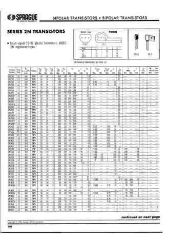
Type Designator: 2N38 📄📄
Material of Transistor: Ge
Polarity: PNP
Absolute Maximum Ratings
Maximum Collector Power Dissipation (Pc): 0.05 W
Maximum Collector-Base Voltage |Vcb|: 20 V
Maximum Collector Current |Ic max|: 0.008 A
Max. Operating Junction Temperature (Tj): 80 °C
Electrical Characteristics
Transition Frequency (ft): 0.2 MHz
Forward Current Transfer Ratio (hFE), MIN: 10
Package: TO22
📄📄 Copy
2N38 Substitution
- BJT ⓘ Cross-Reference Search
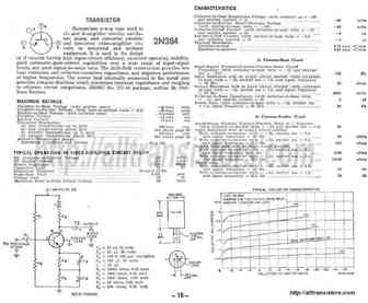
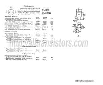
2N38 datasheet
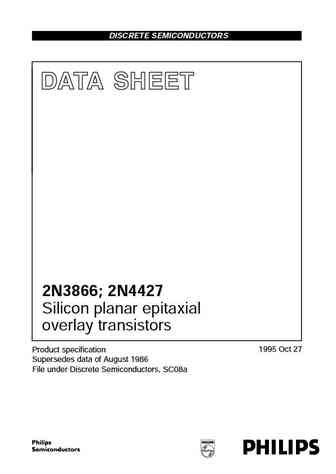
DISCRETE SEMICONDUCTORS DATA SHEET 2N3866; 2N4427 Silicon planar epitaxial overlay transistors 1995 Oct 27 Product specification Supersedes data of August 1986 File under Discrete Semiconductors, SC08a Philips Semiconductors Product specification Silicon planar epitaxial 2N3866; 2N4427 overlay transistors DESCRIPTION APPLICATIONS NPN overlay transistors in TO-39 metal packages wi... See More ⇒
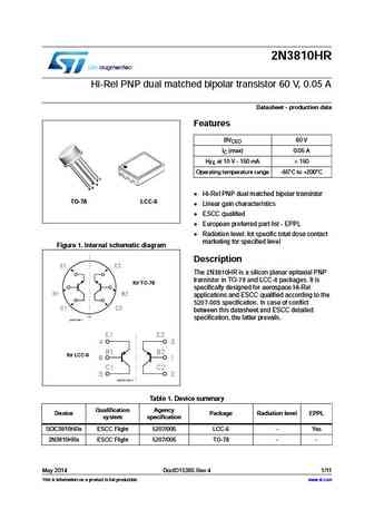
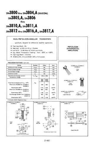
2N3810HR Hi-Rel PNP dual matched bipolar transistor 60 V, 0.05 A Datasheet - production data Features BVCEO 60 V IC (max) 0.05 A HFE at 10 V - 150 mA > 150 Operating temperature range -65 C to +200 C 1 2 3 4 6 5 Hi-Rel PNP dual matched bipolar transistor TO-78 LCC-6 Linear gain characteristics ESCC qualified European preferred part list - EPPL Radiatio... See More ⇒
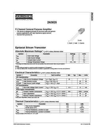
2N3820 P-Channel General Purpose Amplifier This device is designed primarily for low level audio and general purpose applications with high impedance signal sources. Sourced from process 89. TO-92 1 1. Drain 2. Gate 3. Source Epitaxial Silicon Transistor Absolute Maximum Ratings* TC=25 C unless otherwise noted Symbol Parameter Ratings Units VDG Drain-Gate Voltage -20 V VG... See More ⇒
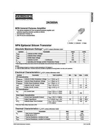
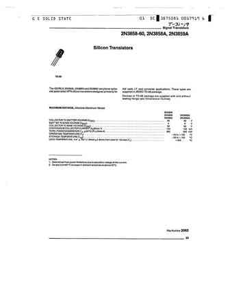
2N3859A NPN General Purpose Amplifier This device designed for use as general purpose amplifier and switches requiring collector currents to 300mA. Sourced from Process 10. See PN100 for characteristics. TO-92 1 1. Emitter 2. Collector 3. Base NPN Epitaxial Silicon Transistor Absolute Maximum Ratings* Ta=25 C unless otherwise noted Symbol Parameter Value Units VCEO C... See More ⇒
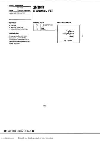
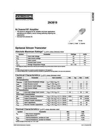
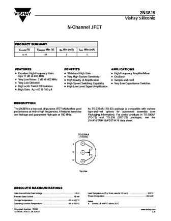
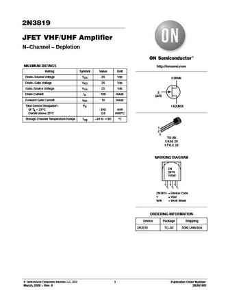
2N3819 N-Channel RF Amplifier This device is designed for RF amplifier and mixer applications operating up to 450MHz, and for analog switching requiring low capacitance. Sourced from process 50. TO-92 1 1. Drain 2. Gate 3. Source Epitaxial Silicon Transistor Absolute Maximum Ratings* TC=25 C unless otherwise noted Symbol Parameter Ratings Units VDG Drain-Gate Voltage 25 ... See More ⇒
2N3819 Vishay Siliconix N-Channel JFET PRODUCT SUMMARY VGS(off) (V) V(BR)GSS Min (V) gfs Min (mS) IDSS Min (mA) v 8 25 2 2 FEATURES BENEFITS APPLICATIONS D Excellent High-Frequency Gain D Wideband High Gain D High-Frequency Amplifier/Mixer Gps 11 dB @ 400 MHz D Very High System Sensitivity D Oscillator D Very Low Noise 3 dB @ 400 MHz D High Quality of Amplification D Sample-a... See More ⇒
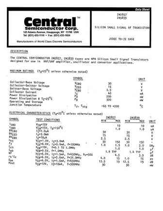
145 Adams Avenue, Hauppauge, NY 11788 USA Tel (631) 435-1110 Fax (631) 435-1824 ... See More ⇒
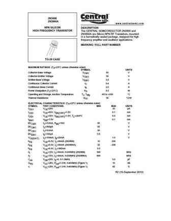
2N3866 2N3866A www.centralsemi.com NPN SILICON DESCRIPTION HIGH FREQUENCY TRANSISTOR The CENTRAL SEMICONDUCTOR 2N3866 and 2N3866A are Silicon NPN RF Transistors, mounted in a hermetically sealed package, designed for high frequency amplifier and oscillator applications. MARKING FULL PART NUMBER TO-39 CASE MAXIMUM RATINGS (TA=25 C unless otherwise noted) SYMBOL UNITS Collec... See More ⇒
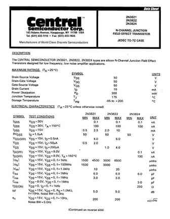
145 Adams Avenue, Hauppauge, NY 11788 USA Tel (631) 435-1110 Fax (631) 435-1824 ... See More ⇒
2N3819 JFET VHF/UHF Amplifier N Channel Depletion MAXIMUM RATINGS http //onsemi.com Rating Symbol Value Unit Drain Source Voltage VDS 25 Vdc 3 DRAIN Drain Gate Voltage VDG 25 Vdc Gate Source Voltage VGS 25 Vdc 2 Drain Current ID 100 mAdc GATE Forward Gate Current IG(f) 10 mAdc Total Device Dissipation PD 1 SOURCE @ TA = 25 C 350 mW Derate above 25 C 2.8 mW/ C St... See More ⇒
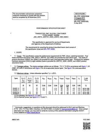
The documentation and process conversion INCH-POUND measures necessary to comply with this revision MIL-PRF-19500/350M shall be completed by 30 November 2015. 31 August 2015 SUPERSEDING MIL-PRF-19500/350L 5 July 2010 PERFORMANCE SPECIFICATION SHEET * TRANSISTOR, PNP, SILICON, LOW POWER TYPES 2N3867, 2N3868, JAN, JANTX, JANTXV, JANS, JANHC, AND JANKC This specification is... See More ⇒
The documentation and process conversion INCH-POUND measures necessary to comply with this revision MIL-PRF-19500/350M shall be completed by 30 November 2015. 31 August 2015 SUPERSEDING MIL-PRF-19500/350L 5 July 2010 PERFORMANCE SPECIFICATION SHEET * TRANSISTOR, PNP, SILICON, LOW POWER TYPES 2N3867, 2N3868, JAN, JANTX, JANTXV, JANS, JANHC, AND JANKC This specification is... See More ⇒
The documentation and process conversion INCH-POUND measures necessary to comply with this revision MIL-PRF-19500/350M shall be completed by 30 November 2015. 31 August 2015 SUPERSEDING MIL-PRF-19500/350L 5 July 2010 PERFORMANCE SPECIFICATION SHEET * TRANSISTOR, PNP, SILICON, LOW POWER TYPES 2N3867, 2N3868, JAN, JANTX, JANTXV, JANS, JANHC, AND JANKC This specification is... See More ⇒
The documentation and process conversion INCH-POUND measures necessary to comply with this revision MIL-PRF-19500/350M shall be completed by 30 November 2015. 31 August 2015 SUPERSEDING MIL-PRF-19500/350L 5 July 2010 PERFORMANCE SPECIFICATION SHEET * TRANSISTOR, PNP, SILICON, LOW POWER TYPES 2N3867, 2N3868, JAN, JANTX, JANTXV, JANS, JANHC, AND JANKC This specification is... See More ⇒
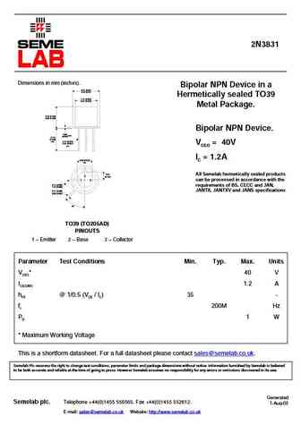
2N3831 Dimensions in mm (inches). Bipolar NPN Device in a 8.51 (0.34) 9.40 (0.37) Hermetically sealed TO39 7.75 (0.305) 8.51 (0.335) Metal Package. 6.10 (0.240) 6.60 (0.260) Bipolar NPN Device. 0.89 max. (0.035) 12.70 (0.500) min. 0.41 (0.016) 0.53 (0.021) VCEO = 40V dia. IC = 1.2A 5.08 (0.200) typ. 2.54 All Semelab hermetically sealed products 2 (0.100) 1 ... See More ⇒
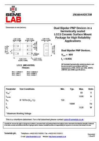
2N3804ADCSM Dimensions in mm (inches). Dual Bipolar PNP Devices in a hermetically sealed LCC2 Ceramic Surface Mount Package for High Reliability 1.40 0.15 2.29 0.20 1.65 0.13 (0.055 0.006) (0.09 0.008) (0.065 0.005) Applications 2 3 1 4 Dual Bipolar PNP Devices. A 0.23 6 5 rad. (0.009) V = 60V CEO 6.22 0.13 A = 1.27 0.13 I = 0.05A C (0... See More ⇒
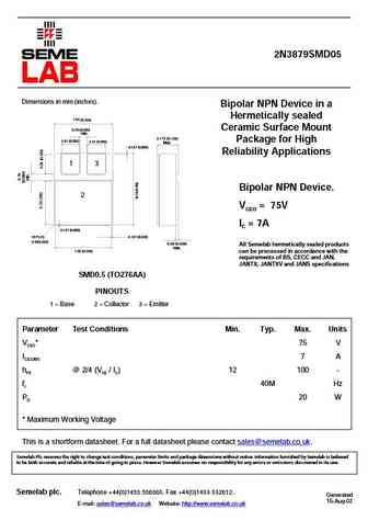
2N3879SMD05 Dimensions in mm (inches). Bipolar NPN Device in a Hermetically sealed 7.54 (0.296) 0.76 (0.030) Ceramic Surface Mount min. 3.175 (0.125) 2.41 (0.095) Package for High 2.41 (0.095) Max. 0.127 (0.005) Reliability Applications 1 3 Bipolar NPN Device. 2 VCEO = 75V IC = 7A 0.127 (0.005) 16 PLCS 0.127 (0.005) 0.50(0.020) 0.50 (0.020) All Semelab herm... See More ⇒
2N3868SMD05 Dimensions in mm (inches). Bipolar PNP Device in a Hermetically sealed 7.54 (0.296) 0.76 (0.030) Ceramic Surface Mount min. 3.175 (0.125) 2.41 (0.095) Package for High 2.41 (0.095) Max. 0.127 (0.005) Reliability Applications 1 3 Bipolar PNP Device. 2 VCEO = 60V IC = 1A 0.127 (0.005) 16 PLCS 0.127 (0.005) 0.50(0.020) 0.50 (0.020) All Semelab herm... See More ⇒
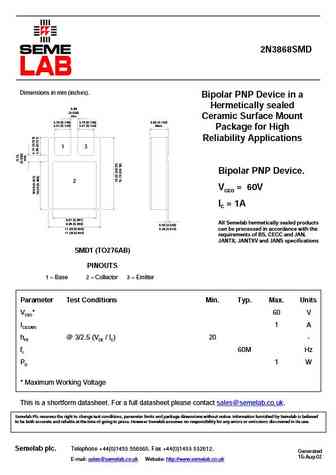
2N3868SMD Dimensions in mm (inches). Bipolar PNP Device in a Hermetically sealed 0.89 (0.035) min. Ceramic Surface Mount 3.70 (0.146) 3.70 (0.146) 3.60 (0.142) 3.41 (0.134) 3.41 (0.134) Max. Package for High Reliability Applications 1 3 Bipolar PNP Device. 2 VCEO = 60V IC = 1A 9.67 (0.381) All Semelab hermetically sealed products 9.38 (0.369) 0.50 (0.020) 0.26 (0... See More ⇒
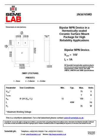
2N3879SMD Dimensions in mm (inches). Bipolar NPN Device in a Hermetically sealed 0.89 (0.035) min. Ceramic Surface Mount 3.70 (0.146) 3.70 (0.146) 3.60 (0.142) 3.41 (0.134) 3.41 (0.134) Max. Package for High Reliability Applications 1 3 Bipolar NPN Device. 2 VCEO = 75V IC = 7A 9.67 (0.381) All Semelab hermetically sealed products 9.38 (0.369) 0.50 (0.020) 0.26 (0... See More ⇒
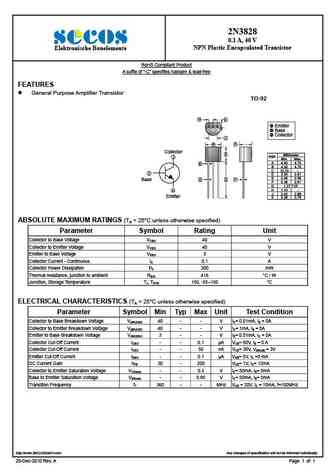
2N3828 0.1 A, 40 V NPN Plastic Encapsulated Transistor Elektronische Bauelemente RoHS Compliant Product A suffix of -C specifies halogen & lead-free FEATURES General Purpose Amplifier Transistor TO-92 G H Emitter Base Collector J A D Collector B Millimeter REF. Min. Max. A 4.40 4.70 K B 4.30 4.70 C 12.70 - D 3.30 3.81 E 0... See More ⇒
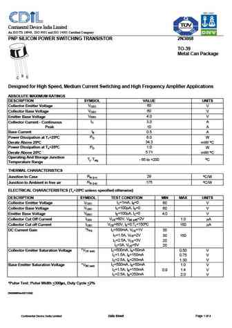
Continental Device India Limited An ISO/TS 16949, ISO 9001 and ISO 14001 Certified Company PNP SILICON POWER SWITCHING TRANSISTOR 2N3868 TO-39 Metal Can Package Designed for High Speed, Medium Current Switching and High Frequency Amplifier Applications ABSOLUTE MAXIMUM RATINGS DESCRIPTION SYMBOL VALUE UNITS VCEO Collector Emitter Voltage 60 V VCBO Collector Base Voltage 60 V VEBO ... See More ⇒
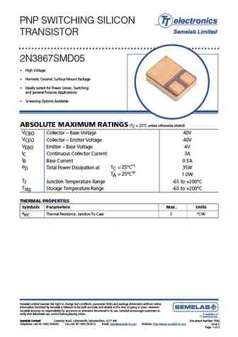
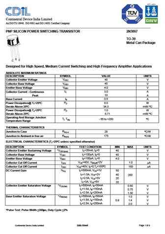
Continental Device India Limited An ISO/TS 16949, ISO 9001 and ISO 14001 Certified Company PNP SILICON POWER SWITCHING TRANSISTOR 2N3867 TO-39 Metal Can Package Designed for High Speed, Medium Current Switching and High Frequency Amplifier Applications ABSOLUTE MAXIMUM RATINGS DESCRIPTION SYMBOL VALUE UNITS VCEO Collector Emitter Voltage 40 V VCBO Collector Base Voltage 40 V VEBO ... See More ⇒
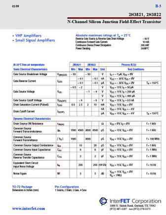
Databook.fxp 1/13/99 2 09 PM Page B-3 01/99 B-3 2N3821, 2N3822 N-Channel Silicon Junction Field-Effect Transistor Absolute maximum ratings at TA = 25 C VHF Amplifiers Reverse Gate Source & Reverse Gate Drain Voltage 50 V Small Signal Amplifiers Continuous Forward Gate Current 10 mA Continuous Device Power Dissipation 300 mW Power Derating 2mW/ C At 25 C free air temperat... See More ⇒
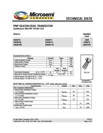
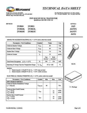
TECHNICAL DATA PNP SILICON DUAL TRANSISTOR Qualified per MIL-PRF-19500/336 Devices Qualified Level 2N3810 2N3811 JAN 2N3810L 2N3811L JANTX 2N3810U 2N3811U JANTXV MAXIMUM RATINGS Ratings Symbol Value Unit Collector-Emitter Voltage 60 Vdc VCEO Collector-Base Voltage 60 Vdc VCBO Emitter-Base Voltage 5.0 Vdc VEBO Collector Current 50 mAdc IC One Both Section 1... See More ⇒
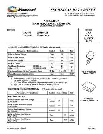
TECHNICAL DATA SHEET 6 Lake Street, Lawrence, MA 01841 Gort Road Business Park, Ennis, Co. Clare, Ireland 1-800-446-1158 / (978) 620-2600 / Fax (978) 689-0803 Tel +353 (0) 65 6840044 Fax +353 (0) 65 6822298 Website http //www.microsemi.com NPN SILICON HIGH-FREQUENCY TRANSISTOR Qualified per MIL-PRF-19500/398 DEVICES LEVELS 2N3866 2N3866UB JAN 2N3866A 2N3866AUB JANTX JANTX... See More ⇒
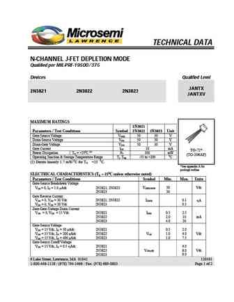
TECHNICAL DATA N-CHANNEL J-FET DEPLETION MODE Qualified per MIL-PRF-19500/375 Devices Qualified Level JANTX 2N3821 2N3822 2N3823 JANTXV MAXIMUM RATINGS 2N3821 Parameters / Test Conditions Symbol 2N3822 2N3823 Unit Gate-Source Voltage VGSR 50 30 V Drain-Source Voltage V 50 30 V DS Drain-Gate Voltage V 50 30 V DG Gate Current I 10 mA GF TO-72* Power Dissipatio... See More ⇒
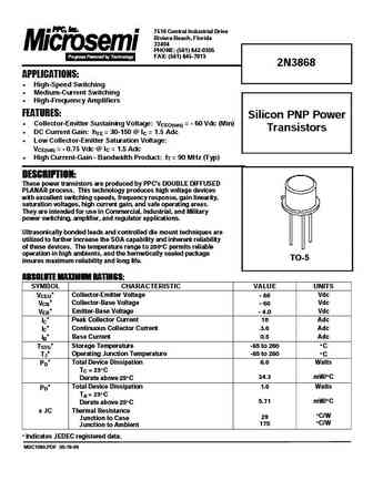
7516 Central Industrial Drive Riviera Beach, Florida 33404 PHONE (561) 842-0305 FAX (561) 845-7813 2N3868 APPLICATIONS High-Speed Switching Medium-Current Switching High-Frequency Amplifiers FEATURES Silicon PNP Power Collector-Emitter Sustaining Voltage VCEO(sus) = - 60 Vdc (Min) Transistors DC Current Gain hFE = 30-150 @ IC = 1.5 Adc Low Collector-... See More ⇒
TECHNICAL DATA SHEET 6 Lake Street, Lawrence, MA 01841 6 Lake Street, Lawrence, MA 01841 Gort Road Business Park, Ennis, Co. Clare, Ireland 1-800-446-1158 / (978) 620-2600 / Fax (978) 689-0803 Tel +353 (0) 65 6840044 Fax +353 (0) 65 6822298 Website http //www.microsemi.com PNP SILICON DUAL TRANSISTOR Qualified per MIL-PRF-19500 /336 DEVICES LEVELS 2N3810 2N3811 JAN 2N3810L ... See More ⇒
TECHNICAL DATA SHEET 6 Lake Street, Lawrence, MA 01841 6 Lake Street, Lawrence, MA 01841 Gort Road Business Park, Ennis, Co. Clare, Ireland 1-800-446-1158 / (978) 620-2600 / Fax (978) 689-0803 Tel +353 (0) 65 6840044 Fax +353 (0) 65 6822298 Website http //www.microsemi.com PNP SILICON DUAL TRANSISTOR Qualified per MIL-PRF-19500 /336 DEVICES LEVELS 2N3810 2N3811 JAN 2N3810L ... See More ⇒
TECHNICAL DATA SHEET 6 Lake Street, Lawrence, MA 01841 6 Lake Street, Lawrence, MA 01841 Gort Road Business Park, Ennis, Co. Clare, Ireland 1-800-446-1158 / (978) 620-2600 / Fax (978) 689-0803 Tel +353 (0) 65 6840044 Fax +353 (0) 65 6822298 Website http //www.microsemi.com PNP SILICON DUAL TRANSISTOR Qualified per MIL-PRF-19500 /336 DEVICES LEVELS 2N3810 2N3811 JAN 2N3810L ... See More ⇒
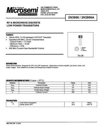
140 COMMERCE DRIVE MONTGOMERYVILLE, PA 18936-1013 PHONE (215) 631-9840 FAX (215) 631-9855 2N3866 / 2N3866A RF & MICROWAVE DISCRETE LOW POWER TRANSISTORS Features Silicon NPN, To-39 packaged VHF/UHF Transistor Specified 400 MHz, 28Vdc Characteristics - Output Power = 1.0 Watt - Minimum Gain = 10 dB - Efficiency = 45% 1. Emitter 800 MHz Current-Gain Bandwidth Produ... See More ⇒
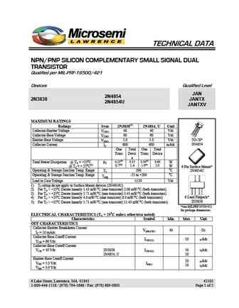
TECHNICAL DATA NPN/PNP SILICON COMPLEMENTARY SMALL SIGNAL DUAL TRANSISTOR Qualified per MIL-PRF-19500/421 Devices Qualified Level JAN 2N4854 2N3838 JANTX 2N4854U JANTXV MAXIMUM RATINGS Ratings Sym 2N3838(2) 2N4854, U Unit Collector-Emitter Voltage 40 40 Vdc VCEO Collector-Base Voltage 60 60 Vdc VCBO Emitter-Base Voltage 5.0 5.0 Vdc TO-78* VEBO 2N4854 Collector ... See More ⇒
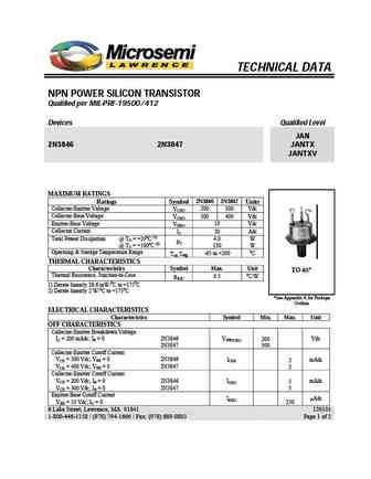
TECHNICAL DATA NPN POWER SILICON TRANSISTOR Qualified per MIL-PRF-19500/412 Devices Qualified Level JAN 2N3846 2N3847 JANTX JANTXV MAXIMUM RATINGS Ratings Symbol 2N3846 2N3847 Units Collector-Emitter Voltage 200 300 Vdc VCEO Collector-Base Voltage 300 400 Vdc VCBO Emitter-Base Voltage 10 Vdc VEBO Collector Current 20 Adc IC Total Power Dissipation @ T = +250C (... See More ⇒
7516 Central Industrial Drive Riviera Beach, Florida 33404 PHONE (561) 842-0305 FAX (561) 845-7813 2N3867 APPLICATIONS High-Speed Switching Medium-Current Switching High-Frequency Amplifiers FEATURES Silicon PNP Power Collector-Emitter Sustaining Voltage VCEO(sus) = - 40 Vdc (Min) Transistors DC Current Gain hFE = 40-200 @ IC = 1.5 Adc Low Collector-... See More ⇒
TECHNICAL DATA SHEET 6 Lake Street, Lawrence, MA 01841 6 Lake Street, Lawrence, MA 01841 Gort Road Business Park, Ennis, Co. Clare, Ireland 1-800-446-1158 / (978) 620-2600 / Fax (978) 689-0803 Tel +353 (0) 65 6840044 Fax +353 (0) 65 6822298 Website http //www.microsemi.com PNP SILICON DUAL TRANSISTOR Qualified per MIL-PRF-19500 /336 DEVICES LEVELS 2N3810 2N3811 JAN 2N3810L ... See More ⇒
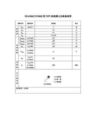
3DA3866(2N3866) NPN PCM Ta=25 5 W ICM 0.4 A Tjm 175 Tstg -55 150 V(BR)CBO IC=0.1mA 55 V V(BR)CEO IC=5.0mA 30 V V(BR)EBO IE=0.1mA 3.5 V ICEO VCE=28V 20 A IC=100mA VCEsat 1 V IB=20mA VCE=5V hFE 25 IC=50m A VCE=15V ... See More ⇒
... See More ⇒
isc Silicon NPN Power Transistor 2N3865 DESCRIPTION Excellent Safe Operating Area Low Collector-Emitter Saturation Voltage 100% avalanche tested Minimum Lot-to-Lot variations for robust device performance and reliable operation. APPLICATIONS Designed for medium-speed switching and amplifier applications. ABSOLUTE MAXIMUM RATINGS(T =25 ) a SYMBOL PARAMETER VALUE UNIT V C... See More ⇒
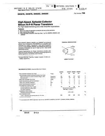
isc Silicon NPN Power Transistor 2N3878 DESCRIPTION Excellent Safe Operating Area Low Collector-Emitter Saturation Voltage 100% avalanche tested Minimum Lot-to-Lot variations for robust device performance and reliable operation. APPLICATIONS Designed for high speed switching and linear- amplifier applications. ABSOLUTE MAXIMUM RATINGS(T =25 ) a SYMBOL PARAMETER VALUE UNI... See More ⇒
isc Silicon NPN Power Transistor 2N3879 DESCRIPTION Excellent Safe Operating Area Low Collector-Emitter Saturation Voltage 100% avalanche tested Minimum Lot-to-Lot variations for robust device performance and reliable operation. APPLICATIONS Designed for high speed switching and linear- amplifier applications. ABSOLUTE MAXIMUM RATINGS(T =25 ) a SYMBOL PARAMETER VALUE UNI... See More ⇒
isc Silicon NPN Power Transistor 2N3863 DESCRIPTION Excellent Safe Operating Area Low Collector-Emitter Saturation Voltage 100% avalanche tested Minimum Lot-to-Lot variations for robust device performance and reliable operation. APPLICATIONS Designed for medium-speed switching and amplifier applications. ABSOLUTE MAXIMUM RATINGS(T =25 ) a SYMBOL PARAMETER VALUE UNIT V C... See More ⇒
isc Silicon NPN Power Transistor 2N3864 DESCRIPTION Excellent Safe Operating Area Low Collector-Emitter Saturation Voltage 100% avalanche tested Minimum Lot-to-Lot variations for robust device performance and reliable operation. APPLICATIONS Designed for medium-speed switching and amplifier applications. ABSOLUTE MAXIMUM RATINGS(T =25 ) a SYMBOL PARAMETER VALUE UNIT V C... See More ⇒
Detailed specifications: 2N3793, 2N3794, 2N3795, 2N3798, 2N3798A, 2N3799, 2N3799A, 2N3799X, BC548, 2N380, 2N3800, 2N3800DCSM, 2N3801, 2N3801DCSM, 2N3802, 2N3802DCSM, 2N3803
Keywords - 2N38 pdf specs
2N38 cross reference
2N38 equivalent finder
2N38 pdf lookup
2N38 substitution
2N38 replacement
BJT Parameters and How They Relate
History: MMUN2113LT1G | FJP5200 | BFV76 | 2SB231 | US6X7 | BC365 | BFV79
🌐 : EN ES РУ
LIST
Last Update
BJT: ZDT6705 | GA1L4Z | GA1A4M | SBT42 | 2SA200-Y | 2SA200-O
Popular searches
c3856 | 30100 transistor | 2sc1675 | k117 transistor | 2sc2291 | bc139 | 2sc1398 | 2sd218
