MA1 datasheet, аналоги, основные параметры
Наименование производителя: MA1 📄📄
Тип материала: Ge
Полярность: PNP
Предельные значения
Максимальная рассеиваемая мощность (Pc): 0.025 W
Макcимально допустимое напряжение коллектор-база (Ucb): 60 V
Макcимально допустимое напряжение коллектор-эмиттер (Uce): 60 V
Макcимальный постоянный ток коллектора (Ic): 0.05 A
Предельная температура PN-перехода (Tj): 75 °C
Электрические характеристики
Ёмкость коллекторного перехода (Cc): 8 pf
Статический коэффициент передачи тока (hFE): 245
Корпус транзистора: TO24
📄📄 Копировать
- подборⓘ биполярного транзистора по параметрам
MA1 даташит
0.1. Size:321K fairchild semi
fdma1028nz.pdf 
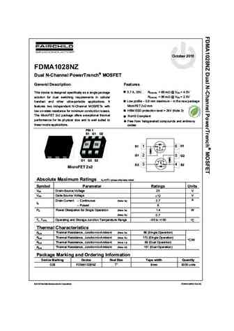
t October 2010 tm FDMA1028NZ Dual N-Channel PowerTrench MOSFET General Description Features 3.7 A, 20V. RDS(ON) = 68 m @ VGS = 4.5V This device is designed specifically as a single package RDS(ON) = 86 m @ VGS = 2.5V solution for dual switching requirements in cellular Low profile 0.8 mm maximum in the new package handset and other ultra-portable
0.2. Size:402K fairchild semi
fdma1024nz.pdf 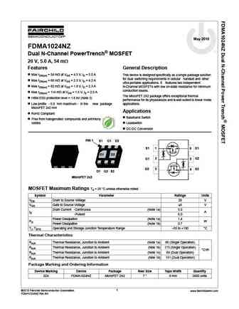
May 2010 FDMA1024NZ Dual N-Channel PowerTrench MOSFET 20 V, 5.0 A, 54 m Features General Description Max rDS(on) = 54 m at VGS = 4.5 V, ID = 5.0 A This device is designed specifically as a single package solution for dual switching requirements in cellular handset and other Max rDS(on) = 66 m at VGS = 2.5 V, ID = 4.2 A ultra-portable applications. It features two indepe
0.3. Size:322K fairchild semi
fdma1430jp.pdf 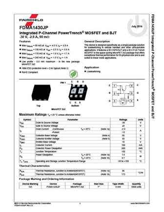
July 2014 FDMA1430JP Integrated P-Channel PowerTrench MOSFET and BJT -30 V, -2.9 A, 90 m Features General Description This device is designed specifically as a single package solution Max rDS(on) = 90 m at VGS = -4.5 V, ID = -2.9 A for loadswitching in cellular handset and other ultra-portable Max rDS(on) = 130 m at VGS = -2.5 V, ID = -2.6 A applications. It features a 50
0.4. Size:374K fairchild semi
fdma1032cz.pdf 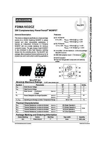
May 2010 FDMA1032CZ tm 20V Complementary PowerTrench MOSFET General Description Features Q1 N-Channel This device is designed specifically as a single package 3.7 A, 20V. RDS(ON) = 68 m @ VGS = 4.5V solution for a DC/DC 'Switching' MOSFET in cellular RDS(ON) = 86 m @ VGS = 2.5V handset and other ultra-portable applications. It Q2 P-Channel features a
0.5. Size:417K fairchild semi
fdma1023pz.pdf 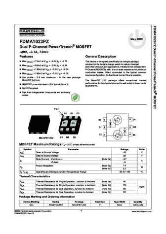
May 2009 FDMA1023PZ tm Dual P-Channel PowerTrench MOSFET 20V, 3.7A, 72m Features General Description Max rDS(on) = 72m at VGS = 4.5V, ID = 3.7A This device is designed specifically as a single package solution for the battery charge switch in cellular handset Max rDS(on) = 95m at VGS = 2.5V, ID = 3.2A and other ultra-portable applications. It features
0.6. Size:379K fairchild semi
fdma1027pt.pdf 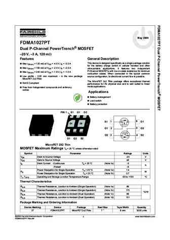
May 2009 FDMA1027PT Dual P-Channel PowerTrench MOSFET 20 V, 3 A, 120 m Features General Description This device is designed specifically as a single package solution Max rDS(on) = 120 m at VGS = -4.5 V, ID = -3.0 A for the battery charge switch in cellular handset and other Max rDS(on) = 160 m at VGS = -2.5 V, ID = -2.5 A ultra-portable applications. It features tw
0.7. Size:339K fairchild semi
fdma1025p.pdf 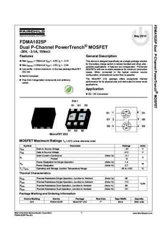
May 20 FDMA1025P tm Dual P-Channel PowerTrench MOSFET 20V, 3.1A, 155m Features General Description Max rDS(on) = 155m at VGS = 4.5V, ID = 3.1A This device is designed specifically as a single package solution for the battery charge switch in cellular handset and other ultra - Max rDS(on) = 220m at VGS = 2.5V, ID = 2.3A portable applications. It feat
0.8. Size:256K fairchild semi
fdma1029pz.pdf 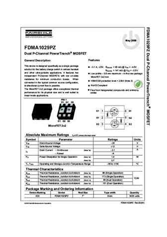
May 2009 tmtm FDMA1029PZ Dual P-Channel PowerTrench MOSFET General Description Features This device is designed specifically as a single package 3.1 A, 20V. RDS(ON) = 95 m @ VGS = 4.5V solution for the battery charge switch in cellular handset RDS(ON) = 141 m @ VGS = 2.5V and other ultra-portable applications. It features two Low profile 0.8 mm maximu
0.9. Size:423K fairchild semi
fdma1027p.pdf 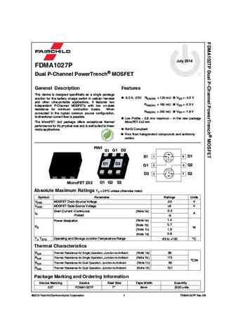
July 2014 FDMA1027P Dual P-Channel PowerTrench MOSFET General Description Features This device is designed specifically as a single package -3.0 A, -20V. RDS(ON) = 120 m @ VGS = -4.5 V solution for the battery charge switch in cellular handset and other ultra-portable applications. It features two RDS(ON) = 160 m @ VGS = -2.5 V independent P-Channel MOSFETs with low on-state
0.10. Size:64K rohm
uma1n uma1n fma1a.pdf 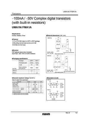
UMA1N / FMA1A Transistors -100mA / -50V Complex digital transistors (with built-in resistors) UMA1N / FMA1A Applications External dimensions (Unit mm) Inverter, Interface, Driver 2.0 UMA1N Features 1.3 0.9 1) Two DTA124E chips in a UMT or SMT package. 0.65 0.65 0.7 2) Mounting cost and area can be cut in half. (5) (4) 3) Emitter-common type. (1) (2) (3) Struct
0.12. Size:35K rohm
uma10n.pdf 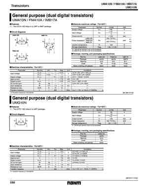
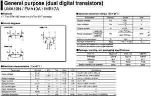
UMA10N / FMA10A / IMB17A Transistors Transistors UMG10N (96-388-A113Z) (94S-811-C113Z) 590
0.13. Size:61K rohm
uma11n.pdf 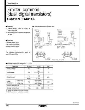
Transistors Emitter common (dual digital transistors) UMA11N / FMA11A FFeatures FExternal dimensions (Units mm) 1) Two DTA143Z chips in a UMT or SMT package. 2) Mounting cost and area can be cut in half. FStructure Epitaxial planar type PNP silicon transistor (Built-in resistor type) The following characteristics apply to both DTr1 and DTr2. FAbsolute maximum ratings (Ta = 25_C)
0.14. Size:62K rohm
uma1n fma1a a1 sot353 sot23-5.pdf 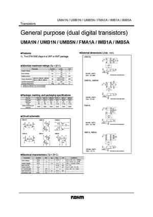
UMA1N / UMB1N / UMB5N / FMA1A / IMB1A / IMB5A Transistors General purpose (dual digital transistors) UMA1N / UMB1N / UMB5N / FMA1A / IMB1A / IMB5A External dimensions (Units mm) Features 1) Two DTA124E chips in a UMT or SMT package. UMA1N 1.25 Absolute maximum ratings (Ta = 25 C) 2.1 Parameter Symbol Limits Unit Supply voltage VCC -50 V 0.1Min. -40 Input voltage VIN V ROHM
0.15. Size:62K rohm
uma11n fma11a a11 sot23-5 sot353.pdf 
Transistors Emitter common (dual digital transistors) UMA11N / FMA11A FFeatures FExternal dimensions (Units mm) 1) Two DTA143Z chips in a UMT or SMT package. 2) Mounting cost and area can be cut in half. FStructure Epitaxial planar type PNP silicon transistor (Built-in resistor type) The following characteristics apply to both DTr1 and DTr2. FAbsolute maximum ratings (Ta = 25_C)
0.16. Size:54K rohm
uma10n fma10a.pdf 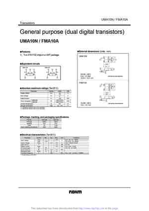
UMA10N / FMA10A Transistors General purpose (dual digital transistors) UMA10N / FMA10A External dimensions (Units mm) Features 1) Two DTA113Z chips in a UMT package. UMA10N 1.25 Equivalent circuits 2.1 UMA10N FMA10A (3) (2) (1) (3) (4) (5) 0.1Min. R1 R1 R1 R1 R2 R2 R2 R2 ROHM UMT5 EIAJ SC-88A Each lead has same dimensions (4) (6) (2) (1) JEDEC SOT-353 FMA10A Abs
0.17. Size:500K onsemi
fdma1025p.pdf 
Is Now Part of To learn more about ON Semiconductor, please visit our website at www.onsemi.com Please note As part of the Fairchild Semiconductor integration, some of the Fairchild orderable part numbers will need to change in order to meet ON Semiconductor s system requirements. Since the ON Semiconductor product management systems do not have the ability to manage part nomenclatur
0.18. Size:123K onsemi
fdma1029pz.pdf 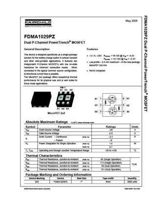
May 2006 FDMA1029PZ Dual P-Channel PowerTrench MOSFET General Description Features This device is designed specifically as a single package 3.1 A, 20V. RDS(ON) = 95 m @ VGS = 4.5V solution for the battery charge switch in cellular handset RDS(ON) = 141 m @ VGS = 2.5V and other ultra-portable applications. It features two Low profile 0.8 mm maxi
0.19. Size:332K htsemi
uma11n.pdf 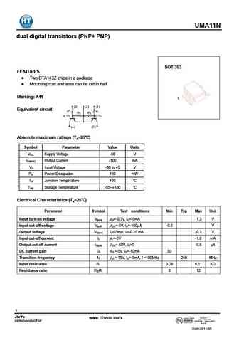
UMA11N dual digital transistors (PNP+ PNP) SOT-353 FEATURES Two DTA143Z chips in a package Mounting cost and area can be cut in half Marking A11 1 Equivalent circuit Absolute maximum ratings (Ta=25 ) Symbol Parameter Value Units VCC Supply Voltage -50 V IC(MAX) Output Current -100 mA Vi Input Voltage -30 to +5 V PD Power Dissipation 150 mW TJ Junction Temperatu
0.22. Size:1007K jilin sino
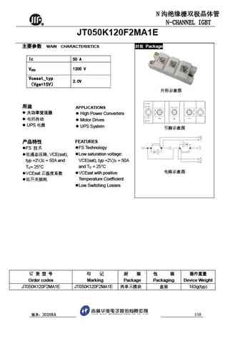
jt050n120f2ma1e.pdf 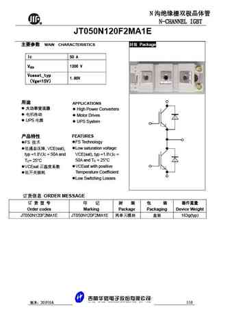
N N-CHANNEL IGBT R IGBT JT050N120F2MA1E MAIN CHARACTERISTICS Package IC 50 A 1200 V V CES Vcesat_typ 1.80V Vge=15V APPLICATIONS High Power Converters Motor Drives UPS UPS System FEATURES FS Technology FS
0.23. Size:913K jilin sino
jt075k120f2ma1e.pdf 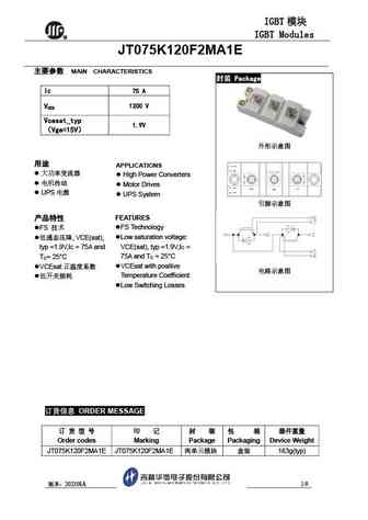
IGBT IGBT Modules R IGBT JT075K120F2MA1E MAIN CHARACTERISTICS Package IC 75 A 1200 V V CES Vcesat_typ 1.9V Vge=15V APPLICATIONS High Power Converters Motor Drives UPS UPS System FEATURES FS Techno
0.24. Size:835K jilin sino
jt075n120f2ma1e.pdf 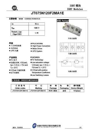
IGBT IGBT Modules R IGBT JT075N120F2MA1E MAIN CHARACTERISTICS Package IC 75 A 1200 V V CES Vcesat_typ 1.9V Vge=15V APPLICATIONS High Power Converters Motor Drives UPS UPS System FEATURES FS Techno
0.25. Size:911K jilin sino
jt100k120f2ma1e.pdf 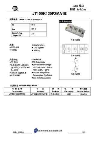
IGBT IGBT Modules R IGBT JT100K120F2MA1E MAIN CHARACTERISTICS Package IC 100 A 1200 V V CES Vcesat_typ 1.9V Vge=15V APPLICATIONS UPS UPS System Welding FEATURES FS Technology FS Low saturation voltage
0.26. Size:916K jilin sino
jt150n120f2ma1e.pdf 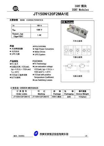
IGBT IGBT Modules R IGBT JT150N120F2MA1E MAIN CHARACTERISTICS Package IC 150 A 1200 V V CES Vcesat_typ 1.8V Vge=15V APPLICATIONS High Power Converters Motor Drives UPS UPS System FEATURES FS Techn
0.27. Size:86K chenmko
chuma1gp.pdf 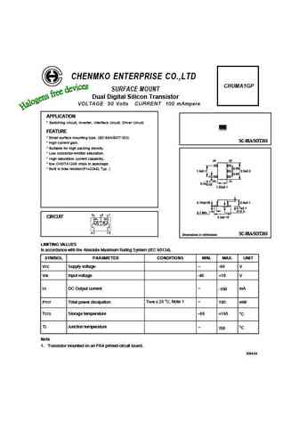
CHENMKO ENTERPRISE CO.,LTD CHUMA1GP SURFACE MOUNT Dual Digital Silicon Transistor VOLTAGE 50 Volts CURRENT 100 mAmpere APPLICATION * Switching circuit, Inverter, Interface circuit, Driver circuit. FEATURE * Small surface mounting type. (SC-88A/SOT-353) SC-88A/SOT353 * High current gain. * Suitable for high packing density. * Low colloector-emitter saturation. * High saturation cu
0.28. Size:173K chenmko
chfma10gp.pdf 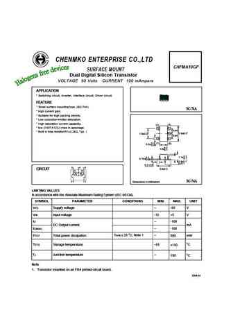
CHENMKO ENTERPRISE CO.,LTD CHFMA10GP SURFACE MOUNT Dual Digital Silicon Transistor VOLTAGE 50 Volts CURRENT 100 mAmpere APPLICATION * Switching circuit, Inverter, Interface circuit, Driver circuit. FEATURE * Small surface mounting type. (SC-74A) SC-74A * High current gain. * Suitable for high packing density. * Low colloector-emitter saturation. * High saturation current capabili
0.29. Size:118K chenmko
chema11gp.pdf 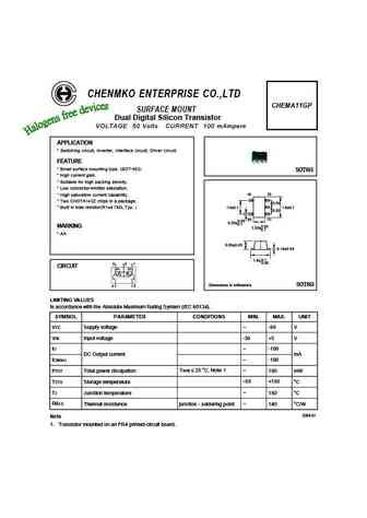
CHENMKO ENTERPRISE CO.,LTD CHEMA11GP SURFACE MOUNT Dual Digital Silicon Transistor VOLTAGE 50 Volts CURRENT 100 mAmpere APPLICATION * Switching circuit, Inverter, Interface circuit, Driver circuit. FEATURE * Small surface mounting type. (SOT-553) SOT553 * High current gain. * Suitable for high packing density. * Low colloector-emitter saturation. (4) (3) * High saturation curren
0.30. Size:181K chenmko
chuma11gp.pdf 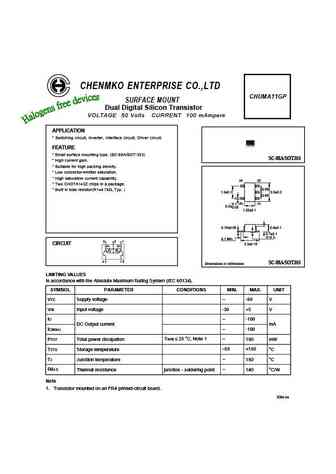
CHENMKO ENTERPRISE CO.,LTD CHUMA11GP SURFACE MOUNT Dual Digital Silicon Transistor VOLTAGE 50 Volts CURRENT 100 mAmpere APPLICATION * Switching circuit, Inverter, Interface circuit, Driver circuit. FEATURE * Small surface mounting type. (SC-88A/SOT-353) SC-88A/SOT353 * High current gain. * Suitable for high packing density. * Low colloector-emitter saturation. * High saturation c
0.31. Size:169K chenmko
chuma10gp.pdf 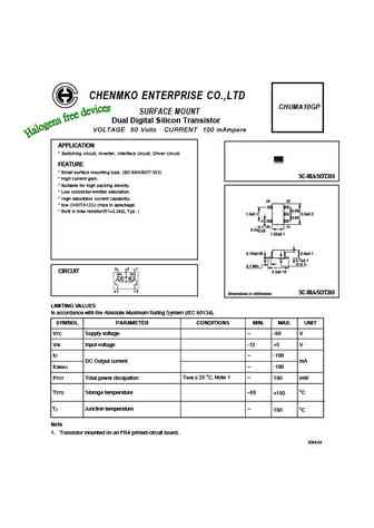
CHENMKO ENTERPRISE CO.,LTD CHUMA10GP SURFACE MOUNT Dual Digital Silicon Transistor VOLTAGE 50 Volts CURRENT 100 mAmpere APPLICATION * Switching circuit, Inverter, Interface circuit, Driver circuit. FEATURE * Small surface mounting type. (SC-88A/SOT-353) SC-88A/SOT353 * High current gain. * Suitable for high packing density. * Low colloector-emitter saturation. * High saturation c
0.32. Size:185K chenmko
chfma11gp.pdf 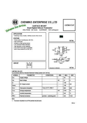
CHENMKO ENTERPRISE CO.,LTD CHFMA11GP SURFACE MOUNT Dual Digital Silicon Transistor VOLTAGE 50 Volts CURRENT 100 mAmpere APPLICATION * Switching circuit, Inverter, Interface circuit, Driver circuit. FEATURE * Small surface mounting type. (SC-74A) SC-74A * High current gain. * Suitable for high packing density. * Low colloector-emitter saturation. * High saturation current capabili
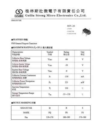
0.33. Size:187K pmc components
pma1516.pdf 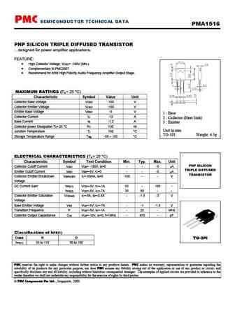
PMA1516 PNP SILICON TRIPLE DIFFUSED TRANSISTOR designed for power amplifier applications. FEATURE High Collector Voltage VCEO= -180V (Min.) Complementary to PMC3907 Recommend for 80W High Fiderity Audio Frequency Amplifier Output Stage. MAXIMUM RATINGS (Ta = 25 C) Characteristic Symbol Value Unit Collector Base Voltage VCBO -180 V Collector Emitter Voltage
0.34. Size:189K pmc components
pma1302.pdf 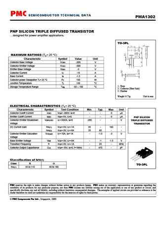
PMA1302 PNP SILICON TRIPLE DIFFUSED TRANSISTOR designed for power amplifier applications. TO-3PL MAXIMUM RATINGS (Ta = 25 C) Characteristic Symbol Value Unit Collector Base Voltage VCBO -200 V Collector Emitter Voltage VCEO -200 V Emitter Base Voltage VEBO -5 V Collector Current IC -15 A Base Current IB -1.5 A Collector power Dissipation Tc= 25 C PC 150 W Junction Tempe
0.35. Size:279K cn wuxi unigroup
tma10n60h.pdf 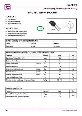
TMA10N60H Wuxi Unigroup Microelectronics Company 600V N-Channel MOSFET FEATURES Fast switching 100% avalanche tested Improved dv/dt capability APPLICATIONS Switch Mode Power Supply (SMPS) Uninterruptible Power Supply (UPS) Power Factor Correction (PFC) Device Marking and Package Information Device Package Marking TMA10N60H TO-220F A10N60H Abs
0.36. Size:250K cn wuxi unigroup
tma12n50h.pdf 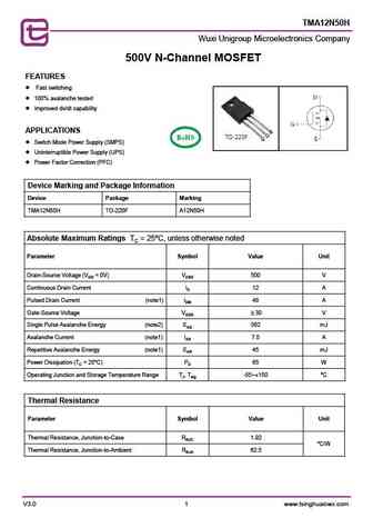
TMA12N50H Wuxi Unigroup Microelectronics Company 500V N-Channel MOSFET FEATURES Fast switching 100% avalanche tested Improved dv/dt capability APPLICATIONS Switch Mode Power Supply (SMPS) Uninterruptible Power Supply (UPS) Power Factor Correction (PFC) Device Marking and Package Information Device Package Marking TMA12N50H TO-220F A12N50H Abs
0.37. Size:340K cn wuxi unigroup
tma10n65h tmp10n65h.pdf 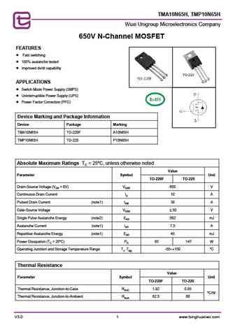
TMA10N65H, TMP10N65H Wuxi Unigroup Microelectronics Company 650V N-Channel MOSFET FEATURES Fast switching 100% avalanche tested Improved dv/dt capability APPLICATIONS Switch Mode Power Supply (SMPS) Uninterruptible Power Supply (UPS) Power Factor Correction (PFC) Device Marking and Package Information Device Package Marking TMA10N65H TO-220F A1
0.38. Size:355K cn wuxi unigroup
tma12n65h tmp12n65h.pdf 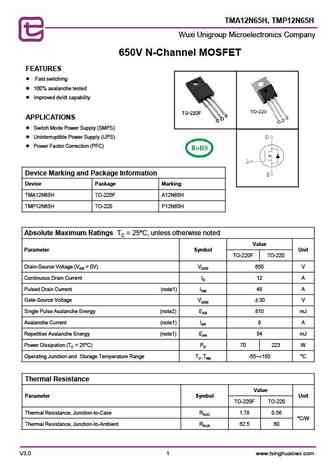
TMA12N65H, TMP12N65H Wuxi Unigroup Microelectronics Company 650V N-Channel MOSFET FEATURES Fast switching 100% avalanche tested Improved dv/dt capability APPLICATIONS Switch Mode Power Supply (SMPS) Uninterruptible Power Supply (UPS) Power Factor Correction (PFC) Device Marking and Package Information Device Package Marking TMA12N65H TO-220F A1
0.39. Size:279K cn wuxi unigroup
tma10n80h.pdf 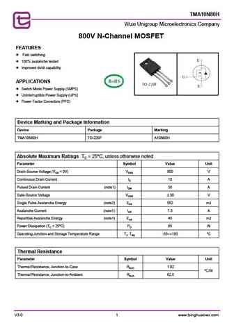
TMA10N80H Wuxi Unigroup Microelectronics Company 800V N-Channel MOSFET FEATURES Fast switching 100% avalanche tested Improved dv/dt capability APPLICATIONS Switch Mode Power Supply (SMPS) Uninterruptible Power Supply (UPS) Power Factor Correction (PFC) Device Marking and Package Information Device Package Marking TMA10N80H TO-220F A10N80H Abs
Другие транзисторы: MA0413, MA0414, MA0461, MA0462, MA0463, MA0491, MA0492, MA0493, A1013, MA100, MA112, MA113, MA114, MA115, MA116, MA117, MA1702