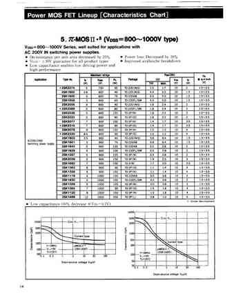
1601 datasheet, аналоги, основные параметры
Наименование производителя: 1601 📄📄
Тип материала: Si
Полярность: PNP
Предельные значения
Максимальная рассеиваемая мощность (Pc): 0.6 W
Макcимально допустимое напряжение коллектор-база (Ucb): 30 V
Макcимально допустимое напряжение коллектор-эмиттер (Uce): 25 V
Макcимально допустимое напряжение эмиттер-база (Ueb): 4 V
Макcимальный постоянный ток коллектора (Ic): 0.05 A
Предельная температура PN-перехода (Tj): 150 °C
Электрические характеристики
Статический коэффициент передачи тока (hFE): 110
Корпус транзистора: TO92
📄📄 Копировать
Аналоги (замена) для 1601
- подборⓘ биполярного транзистора по параметрам
1601 даташит
0.1. Size:362K motorola
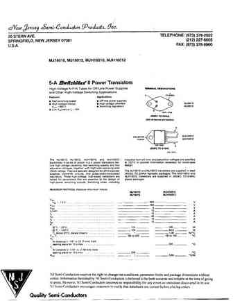
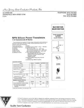
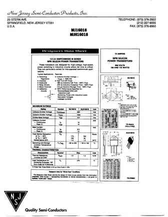
mjw16010.pdf 
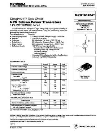
Order this document MOTOROLA by MJW16010A/D SEMICONDUCTOR TECHNICAL DATA MJW16010A * Designer's Data Sheet *Motorola Preferred Device NPN Silicon Power Transistors POWER TRANSISTORS 1 kV SWITCHMODE Series 15 AMPERES 500 VOLTS These transistors are designed for high voltage, high speed, power switching in 125 AND 175 WATTS inductive circuits where fall time is critical. The
0.2. Size:548K motorola
mj16010r.pdf 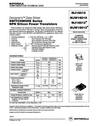
Order this document MOTOROLA by MJ16010/D SEMICONDUCTOR TECHNICAL DATA MJ16010 Designer's Data Sheet MJW16010 SWITCHMODE Series MJ16012* NPN Silicon Power Transistors These transistors are designed for high voltage, high speed, power switching in MJW16012* inductive circuits where fall time is critical. They are particularly suited for line operated switchmode applications
0.3. Size:366K motorola
mj16018r.pdf 
Order this document MOTOROLA by MJ16018/D SEMICONDUCTOR TECHNICAL DATA * MJ16018 * MJW16018 Designer's Data Sheet *Motorola Preferred Device NPN Silicon Power Transistors POWER TRANSISTORS 1.5 kV SWITCHMODE Series 10 AMPERES These transistors are designed for high voltage, high speed, power switching in 800 VOLTS inductive circuits where fall time is critical. They are par
0.4. Size:72K philips
plb16012u 2.pdf 
DISCRETE SEMICONDUCTORS DATA SHEET PLB16012U NPN microwave power transistor 1997 Feb 18 Product specification Supersedes data of November 1994 Philips Semiconductors Product specification NPN microwave power transistor PLB16012U FEATURES QUICK REFERENCE DATA Microwave performance up to Tmb =25 C in a common base class C Input matching cell allows an easier narrowband amplifier
0.5. Size:142K toshiba
rn1601-rn1606.pdf 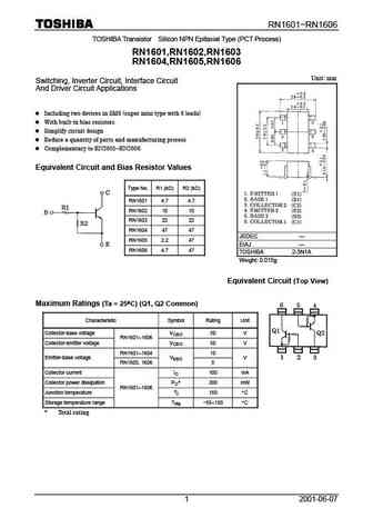
RN1601 RN1606 TOSHIBA Transistor Silicon NPN Epitaxial Type (PCT Process) RN1601,RN1602,RN1603 RN1604,RN1605,RN1606 Unit mm Switching, Inverter Circuit, Interface Circuit And Driver Circuit Applications Including two devices in SM6 (super mini type with 6 leads) With built-in bias resistors Simplify circuit design Reduce a quantity of parts and manufacturing process
0.6. Size:131K renesas
rej03g1601 h7p1002dldsds.pdf 
To our customers, Old Company Name in Catalogs and Other Documents On April 1st, 2010, NEC Electronics Corporation merged with Renesas Technology Corporation, and Renesas Electronics Corporation took over all the business of both companies. Therefore, although the old company name remains in this document, it is a valid Renesas Electronics document. We appreciate your understanding.
0.12. Size:640K infineon
6ms16017e33w32831.pdf 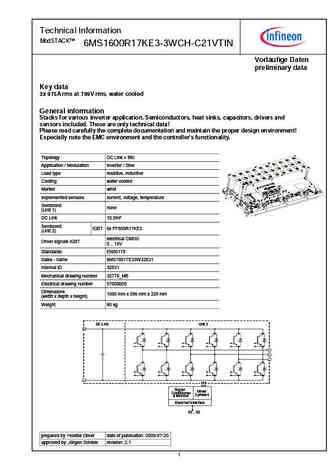
Technical Information ModSTACK 6MS1600R17KE3-3WCH-C21VTIN Vorl ufige Daten preliminary data Key data 3x 975A rms at 789V rms, water cooled General information Stacks for various inverter application. Semiconductors, heat sinks, capacitors, drivers and sensors included. These are only technical data! Please read carefully the complete documentation and maintain the proper design en
0.13. Size:604K infineon
6ms16017e33w32779.pdf 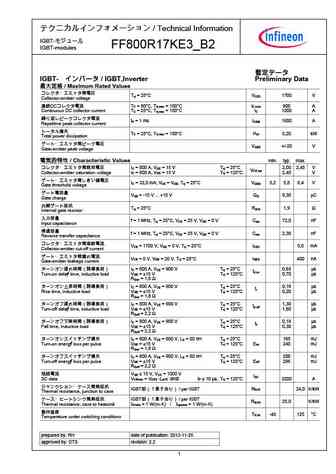
/ Technical Information IGBT- FF800R17KE3_B2 IGBT-modules IGBT- / IGBT,Inverter Preliminary Data / Maximum Rated Values T = 25 C V 1700 V vj CES Collector-emitter voltage DC T = 80 C, T = 150 C I 800 A C vj max C nom
0.14. Size:605K infineon
6ms16017e33w32630.pdf 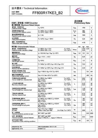
/ Technical Information IGBT- FF800R17KE3_B2 IGBT-modules IGBT, / IGBT,Inverter Preliminary Data / Maximum Rated Values T = 25 C V 1700 V vj CES Collector-emitter voltage T = 80 C, T = 150 C I 800 A C vj max C nom Continuous DC collector current T = 25 C, T = 150 C
0.15. Size:410K onsemi
nst1601cl.pdf 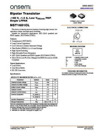
DATA SHEET www.onsemi.com Bipolar Transistor -160 V, -1.5 A, Low VCE(sat) PNP Single LFPAK LFPAK8 3.3x3.3, 0.65P CASE 760AD NST1601CL ELECTRICAL CONNECTION This device is bipolar junction transistor featuring high current, low C 5, 6, 7, 8 saturation voltage, and high speed switching. Suitable for automotive applications. AEC-Q101 qualified and PPAP capable. (NSVT1601CLTWG) Featur
0.16. Size:403K panasonic
fc591601.pdf 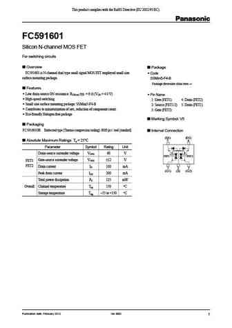
This product complies with the RoHS Directive (EU 2002/95/EC). FC591601 Silicon N-channel MOS FET For switching circuits Overview Package FC591601 is N-channel dual type small signal MOS FET employed small size Code surface mounting package. SSMini5-F4-B Package dimension clicks here. Click! Features Low drain-source ON resistance RDS(on) typ. = 6 W (VGS = 4.
0.17. Size:418K panasonic
fc551601.pdf 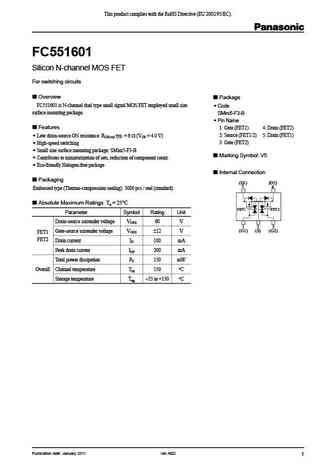
This product complies with the RoHS Directive (EU 2002/95/EC). FC551601 Silicon N-channel MOS FET For switching circuits Overview Package FC551601 is N-channel dual type small signal MOS FET employed small size Code surface mounting package. SMini5-F3-B Pin Name Features 1 Gate (FET1) 4 Drain (FET2) 2 Source (FET1/2) 5 Drain (FET1) Low drain-source ON
0.18. Size:679K cree
c2m0160120d.pdf 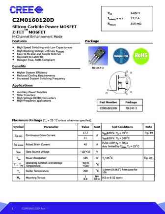
VDS 1200 V ID(MAX) @ 25 C 17.7 A C2M0160120D RDS(on) 160 m Silicon Carbide Power MOSFET TM Z-FET MOSFET N-Channel Enhancement Mode Features Package High Speed Switching with Low Capacitances High Blocking Voltage with Low RDS(on) Easy to Parallel and Simple to Drive Resistant to Latch-Up Halogen Free, RoHS Compliant Benefits TO-247-3 Higher Syst
0.20. Size:113K savantic
mj16018-1400v.pdf 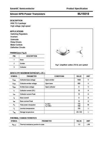
SavantIC Semiconductor Product Specification Silicon NPN Power Transistors MJ16018 DESCRIPTION With TO-3 package High voltage ,high speed APPLICATIONS Switching Regulators Inverters Solenoids Relay Drivers Motor Controls Deflection Circuits PINNING(see Fig.2) PIN DESCRIPTION 1 Base 2 Emitter Fig.1 simplified outline (TO-3) and symbol 3 Collector
0.21. Size:156K jmnic
2sa1601.pdf 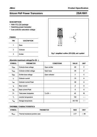
JMnic Product Specification Silicon PNP Power Transistors 2SA1601 DESCRIPTION With ITO-220 package Switching power transistor Low collector saturation voltage PINNING PIN DESCRIPTION 1 Base 2 Collector Fig.1 simplified outline (ITO-220) and symbol 3 Emitter Absolute maximum ratings(Ta=25 ) SYMBOL PARAMETER CONDITIONS VALUE UNIT VCBO Collector-base voltage Open emi
0.22. Size:82K jmnic
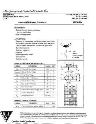
mj16010.pdf 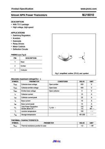
Product Specification www.jmnic.com Silicon NPN Power Transistors MJ16010 DESCRIPTION With TO-3 package High voltage ,high speed APPLICATIONS Switching Regulators Inverters Solenoids Relay Drivers Motor Controls Deflection Circuits PINNING (see Fig.2) PIN DESCRIPTION 1 Base 2 Emitter 3 Collector Fig.1 simplified outline (TO-3) and symbol Absolute
0.23. Size:298K shindengen
2sa1601.pdf 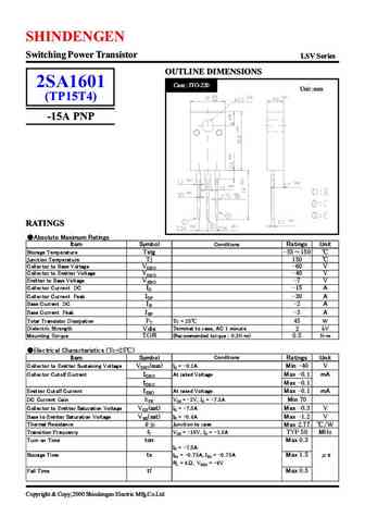
SHINDENGEN Switching Power Transistor LSV Series OUTLINE DIMENSIONS 2SA1601 Case ITO-220 Unit mm (TP15T4) -15A PNP RATINGS
0.24. Size:2281K goford
g1601.pdf 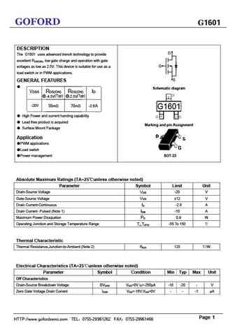
GOFORD G1601 DESCRIPTION D The G1601 uses advanced trench technology to provide excellent RDS(ON), low gate charge and operation with gate G voltages as low as 2.5V. This device is suitable for use as a load switch or in PWM applications. S GENERAL FEATURES Schematic diagram VDSS RDS(ON) RDS(ON) ID (Typ) @ (Typ) @-2.5V -4.5V -20V 55m 70m -2.6 A G1601
0.25. Size:856K basicsemi
b1m160120hc.pdf 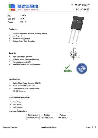
B1M160120HC SiC MOSFET V 1200 V DS I (Tc=25 C) 20 A D R 160 m DS(on) Features Low On-Resistance with High Blocking Voltage Low Capacitance Avalanche Ruggedness Halogen Free, Rohs Compliant 1 2 3 Benefits High Frequency Operation Enabling higher switching frequency Increased power density Reduction of Heat Sink Requirement
0.26. Size:210K inchange semiconductor
2sa1601.pdf 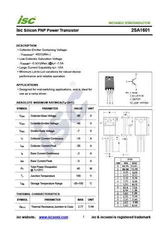
isc Silicon PNP Power Transistor 2SA1601 DESCRIPTION Collector-Emitter Sustaining Voltage- V = -40(V)(Min.) CEO(SUS) Low Collector Saturation Voltage V = -0.3(V)(Max.)@I = -7.5A CE(sat) C Large Current Capability-I = -15A C Minimum Lot-to-Lot variations for robust device performance and reliable operation APPLICATIONS Designed for mid-switching applications, and is ide
0.27. Size:220K inchange semiconductor
mjw16010.pdf 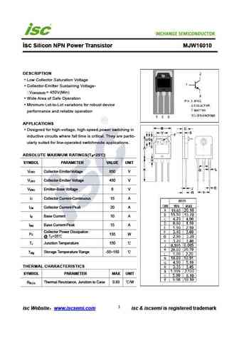
isc Silicon NPN Power Transistor MJW16010 DESCRIPTION Low Collector Saturation Voltage Collector-Emitter Sustaining Voltage- V = 450V(Min) CEO(SUS) Wide Area of Safe Operation Minimum Lot-to-Lot variations for robust device performance and reliable operation APPLICATIONS Designed for high-voltage, high-speed,power switching in inductive circuits where fall time is critica
0.28. Size:207K inchange semiconductor
mj16018.pdf 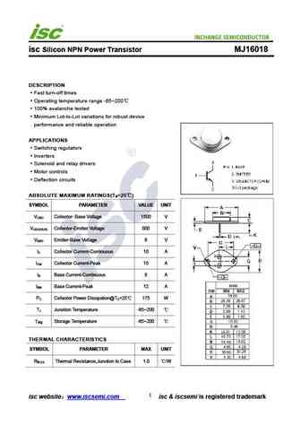
isc Silicon NPN Power Transistor MJ16018 DESCRIPTION Fast turn-off times Operating temperature range -65 200 100% avalanche tested Minimum Lot-to-Lot variations for robust device performance and reliable operation APPLICATIONS Switching regulators Inverters Solenoid and relay drivers Motor controls Deflection circuits ABSOLUTE MAXIMUM RATINGS(T =25 ) a SYMB
0.29. Size:206K inchange semiconductor
mj16012.pdf 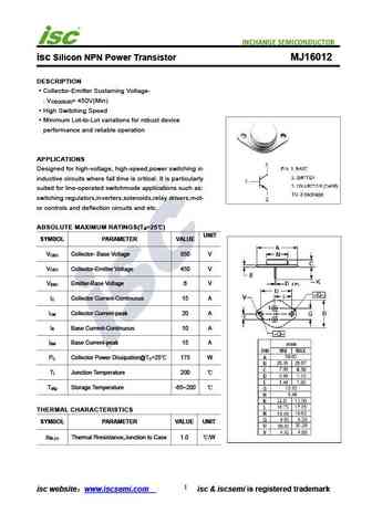
isc Silicon NPN Power Transistor MJ16012 DESCRIPTION Collector-Emitter Sustaining Voltage- V = 450V(Min) CEO(SUS) High Switching Speed Minimum Lot-to-Lot variations for robust device performance and reliable operation APPLICATIONS Designed for high-voltage, high-speed,power switching in inductive circuits where fall time is critical. It is particularly suited for line-operate
0.30. Size:210K inchange semiconductor
2sd1601.pdf 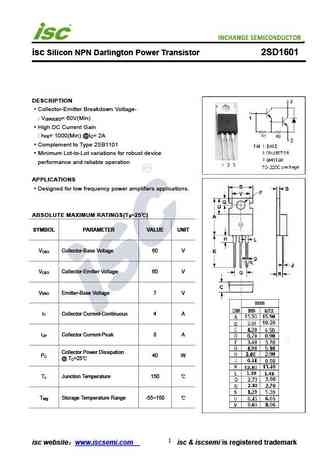
isc Silicon NPN Darlington Power Transistor 2SD1601 DESCRIPTION Collector-Emitter Breakdown Voltage- V = 60V(Min) (BR)CEO High DC Current Gain h = 1000(Min) @I = 2A FE C Complement to Type 2SB1101 Minimum Lot-to-Lot variations for robust device performance and reliable operation APPLICATIONS Designed for low frequency power amplifiers applications. ABSOLUTE MAXIMUM RA
0.31. Size:206K inchange semiconductor
mj16010.pdf 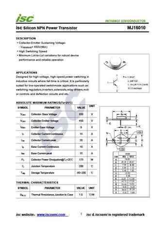
isc Silicon NPN Power Transistor MJ16010 DESCRIPTION Collector-Emitter Sustaining Voltage- V = 450V(Min) CEO(SUS) High Switching Speed Minimum Lot-to-Lot variations for robust device performance and reliable operation APPLICATIONS Designed for high-voltage, high-speed,power switching in inductive circuits where fall time is critical. It is particularly suited for line-operate
0.32. Size:200K inchange semiconductor
pmd1601k.pdf 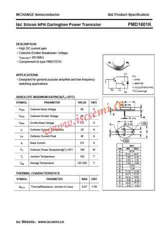
INCHANGE Semiconductor isc Product Specification isc Silicon NPN Darlingtion Power Transistor PMD1601K DESCRIPTION High DC current gain Collector-Emitter Breakdown Voltage- V(BR)CEO= 60V(Min) Complement to type PMD1701K APPLICATIONS Designed for general purpose amplifier and low frequency switching applications ABSOLUTE MAXIMUM RATINGS(TC=25 ) SYMBOL PARAMETER VA
0.33. Size:211K inchange semiconductor
mj16016.pdf 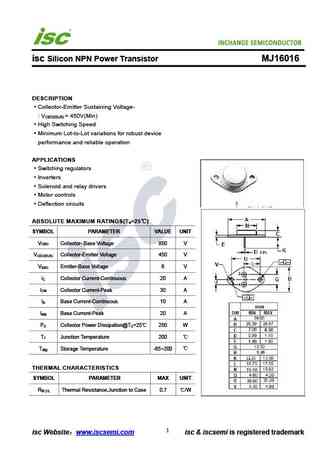
isc Silicon NPN Power Transistor MJ16016 DESCRIPTION Collector-Emitter Sustaining Voltage- V = 450V(Min) CEO(SUS) High Switching Speed Minimum Lot-to-Lot variations for robust device performance and reliable operation APPLICATIONS Switching regulators Inverters Solenoid and relay drivers Motor controls Deflection circuits ABSOLUTE MAXIMUM RATINGS(T =25 ) a SY
0.34. Size:206K inchange semiconductor
mj16014.pdf 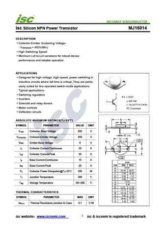
isc Silicon NPN Power Transistor MJ16014 DESCRIPTION Collector-Emitter Sustaining Voltage- V = 450V(Min) CEO(SUS) High Switching Speed Minimum Lot-to-Lot variations for robust device performance and reliable operation APPLICATIONS Designed for high-voltage ,high-speed, power switching in inductive circuits where fall time is critical. They are partic- ularly suited for line
0.35. Size:219K inchange semiconductor
mjw16010a.pdf 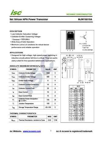
isc Silicon NPN Power Transistor MJW16010A DESCRIPTION Low Collector Saturation Voltage Collector-Emitter Sustaining Voltage- V = 500V(Min) CEO(SUS) Wide Area of Safe Operation Minimum Lot-to-Lot variations for robust device performance and reliable operation APPLICATIONS Designed for high-voltage, high-speed,power switching in inductive circuits where fall time is critic
0.36. Size:215K inchange semiconductor
2sk1601.pdf 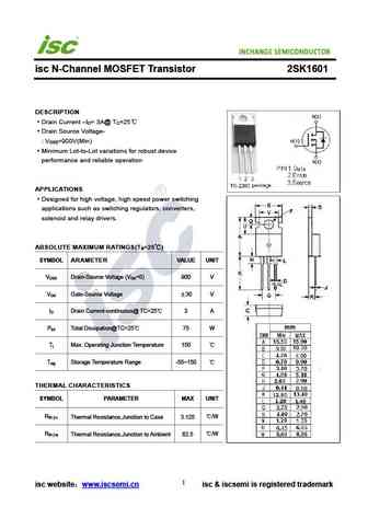
isc N-Channel MOSFET Transistor 2SK1601 DESCRIPTION Drain Current I = 3A@ T =25 D C Drain Source Voltage- V =900V(Min) DSS Minimum Lot-to-Lot variations for robust device performance and reliable operation APPLICATIONS Designed for high voltage, high speed power switching applications such as switching regulators, converters, solenoid and relay drivers. ABSOLUTE MAX
0.37. Size:220K inchange semiconductor
mjw16018.pdf 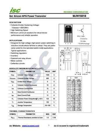
isc Silicon NPN Power Transistor MJW16018 DESCRIPTION Collector-Emitter Sustaining Voltage- V = 800V(Min) CEO(SUS) High Switching Speed Minimum Lot-to-Lot variations for robust device performance and reliable operation APPLICATIONS Designed for high-voltage ,high-speed, power switching in inductive circuits where fall time is critical. They are partic- ularly suited for lin
0.38. Size:219K inchange semiconductor
mjh16018.pdf 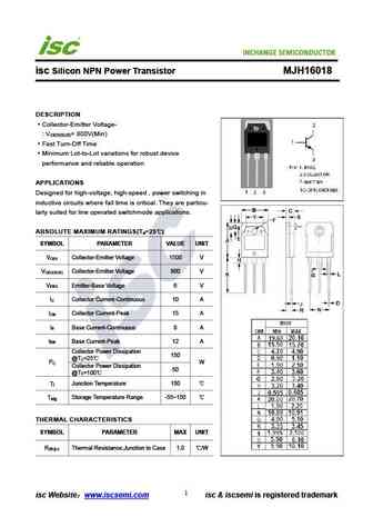
isc Silicon NPN Power Transistor MJH16018 DESCRIPTION Collector-Emitter Voltage- V = 800V(Min) CEO(SUS) Fast Turn-Off Time Minimum Lot-to-Lot variations for robust device performance and reliable operation APPLICATIONS Designed for high-voltage, high-speed , power switching in inductive circuits where fall time is critical. They are particu- larly suited for line operated swi
Другие транзисторы: 1402, 142T2, 1501, 1502, 152NU70, 153NU70, 154NU70, 155NU70, MJE340, 1602, 16029, 16039, 16207, 16207B, 16298, 16299, 16300