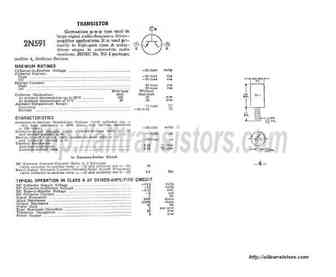
2N59. Аналоги и основные параметры
Наименование производителя: 2N59
Тип материала: Ge
Полярность: PNP
Предельные значения
Максимальная рассеиваемая мощность (Pc): 0.18 W
Макcимально допустимое напряжение коллектор-база (Ucb): 25 V
Макcимально допустимое напряжение эмиттер-база (Ueb): 10 V
Макcимальный постоянный ток коллектора (Ic): 0.2 A
Предельная температура PN-перехода (Tj): 85 °C
Электрические характеристики
Граничная частота коэффициента передачи тока (ft): 0.8 MHz
Ёмкость коллекторного перехода (Cc): 80 pf
Статический коэффициент передачи тока (hFE): 90
Корпус транзистора: TO5
Аналоги (замена) для 2N59
- подборⓘ биполярного транзистора по параметрам
2N59 даташит

2n5951.pdf

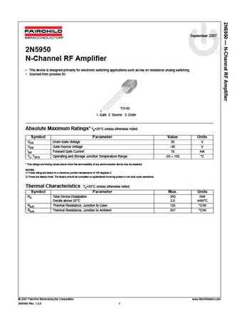
September 2007 2N5951 N-Channel RF Amplifier This device is designed primarily for electronic switching applications such as low on resistance analog switching. Sourced from process 50. TO-92 1 1. Gate 2. Source 3. Drain Absolute Maximum Ratings* Ta=25 C unless otherwise noted Symbol Parameter Value Units VDG Drain-Gate Voltage 30 V VGS Gate-Source Voltage -30 V IGF Forward
2n5961.pdf

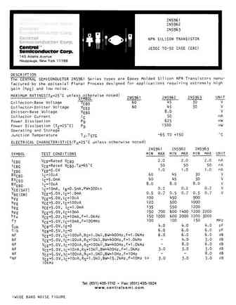
Discrete POWER & Signal Technologies 2N5961 C TO-92 B E NPN General Purpose Amplifier This device is designed for use as low noise, high gain, general purpose amplifiers requiring collector currents to 50 mA. Sourced from Process 07. See 2N5088 for characteristics. Absolute Maximum Ratings* TA = 25 C unless otherwise noted Symbol Parameter Val60ue Units VCEO Collector-Emitter Volta
2n5950.pdf
September 2007 2N5950 N-Channel RF Amplifier This device is designed primarily for electronic switching applications such as low on resistance analog switching. Sourced from process 50. TO-92 1 1. Gate 2. Source 3. Drain Absolute Maximum Ratings* Ta=25 C unless otherwise noted Symbol Parameter Value Units VDG Drain-Gate Voltage 30 V VGS Gate-Source Voltage -30 V IGF Forward
2n5962 mmbt5962.pdf

Discrete POWER & Signal Technologies 2N5962 MMBT5962 C E C TO-92 B B E SOT-23 Mark 117 NPN General Purpose Amplifier This device is designed for use as low noise, high gain, general purpose amplifiers requiring collector currents to 50 mA. Sourced from Process 07. See 2N5088 for characteristics. Absolute Maximum Ratings* TA = 25 C unless otherwise noted Symbol Parameter Value U
2n5952.pdf
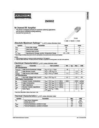
2N5952 N-Channel RF Ampifier This device is designed primarily for electronic switching applications such as low on resistance analog switching. Sourced from process 50. TO-92 1 1. Gate 2. Source 3. Drain Absolute Maximum Ratings * TC=25 C unless otherwise noted Symbol Parameter Value Units VDG Drain-Gate Voltage 30 V VGS Gate-Source Voltage -30 V IGF Forward Gate Current
2n5911 2n5912.pdf

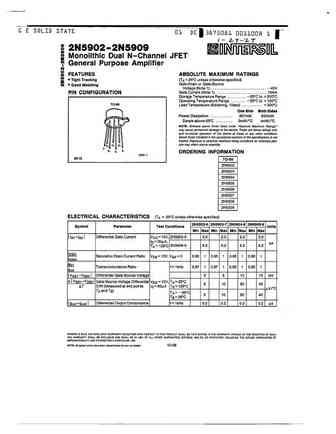
2N5911/5912 Vishay Siliconix Matched N-Channel JFET Pairs PRODUCT SUMMARY Part Number VGS(off) (V) V(BR)GSS Min (V) gfs Min (mS) IG Typ (pA) jVGS1 VGS2j Max (mV) 2N5911 1 to 5 25 5 1 10 2N5912 1 to 5 25 5 1 15 FEATURES BENEFITS APPLICATIONS D Two-Chip Design D Minimum Parasitics Ensuring Maximum D Wideband Differential Amps High-Frequency Performance D High
2n5910 pn5910 2n5771.pdf
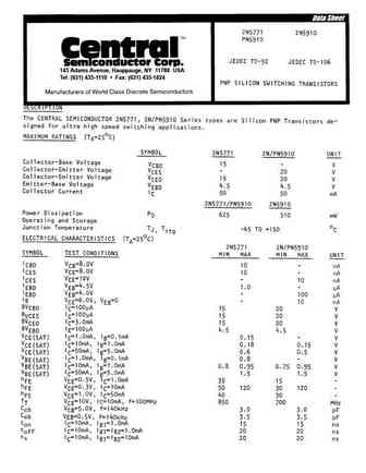
145 Adams Avenue, Hauppauge, NY 11788 USA Tel (631) 435-1110 Fax (631) 435-1824
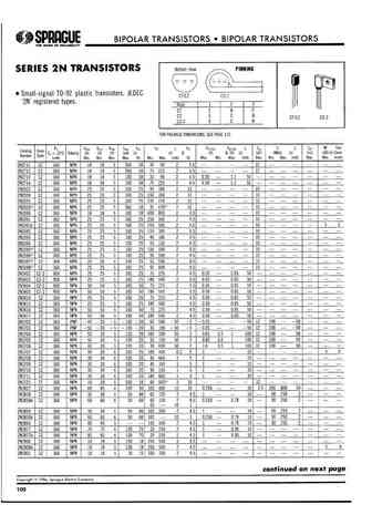
2n5954 2n5955 2n5956 2n6372 2n6373 2n6374.pdf
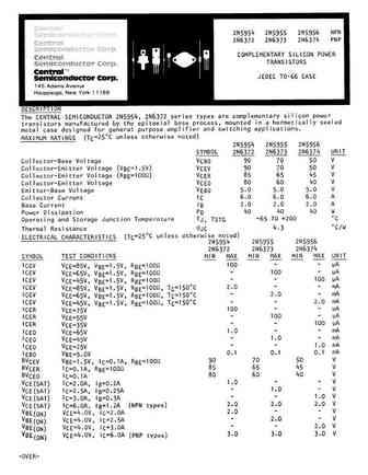
TM Central Semiconductor Corp. 145 Adams Avenue Hauppauge, NY 11788 USA Tel (631) 435-1110 Fax (631) 435-1824 www.centralsemi.com
2n5961 2n5962 2n5963.pdf
Tel (631) 435-1110 Fax (631) 435-1824 www. cent ral semi . com
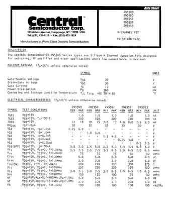
2n5949 2n5950 2n5951 2n5952 2n5953.pdf
145 Adams Avenue, Hauppauge, NY 11788 USA Tel (631) 435-1110 Fax (631) 435-1824
2n5937.pdf

2N5937 Dimensions in mm (inches). Bipolar NPN Device in a Hermetically sealed TO3 25.15 (0.99) 6.35 (0.25) 26.67 (1.05) 9.15 (0.36) Metal Package. 10.67 (0.42) 11.18 (0.44) 1.52 (0.06) 3.43 (0.135) 1 2 Bipolar NPN Device. 3 VCEO = 160V (case) 3.84 (0.151) 4.09 (0.161) 7.92 (0.312) IC = 30A 12.70 (0.50) All Semelab hermetically sealed products can be processed in
2n5935.pdf

2N5935 Dimensions in mm (inches). Bipolar NPN Device in a Hermetically sealed TO3 25.15 (0.99) 6.35 (0.25) 26.67 (1.05) 9.15 (0.36) Metal Package. 10.67 (0.42) 11.18 (0.44) 1.52 (0.06) 3.43 (0.135) 1 2 Bipolar NPN Device. 3 VCEO = 80V (case) 3.84 (0.151) 4.09 (0.161) 7.92 (0.312) IC = 30A 12.70 (0.50) All Semelab hermetically sealed products can be processed in a
2n5934.pdf

2N5934 Dimensions in mm (inches). Bipolar NPN Device in a Hermetically sealed TO3 25.15 (0.99) 6.35 (0.25) 26.67 (1.05) 9.15 (0.36) Metal Package. 10.67 (0.42) 11.18 (0.44) 1.52 (0.06) 3.43 (0.135) 1 2 Bipolar NPN Device. 3 VCEO = 140V (case) 3.84 (0.151) 4.09 (0.161) 7.92 (0.312) IC = 30A 12.70 (0.50) All Semelab hermetically sealed products can be processed in
2n5956.pdf
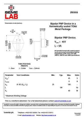
2N5956 Dimensions in mm (inches). Bipolar PNP Device in a Hermetically sealed TO66 6.35 (0.250) Metal Package. 8.64 (0.340) 3.68 (0.145) rad. 3.61 (0.142) max. 4.08(0.161) rad. Bipolar PNP Device. 1 2 VCEO = 45V IC = 6A All Semelab hermetically sealed products can be processed in accordance with the requirements of BS, CECC and JAN, JANTX, JANTXV and JANS specif
2n5930.pdf

2N5930 Dimensions in mm (inches). Bipolar NPN Device in a Hermetically sealed TO3 25.15 (0.99) 6.35 (0.25) 26.67 (1.05) 9.15 (0.36) Metal Package. 10.67 (0.42) 11.18 (0.44) 1.52 (0.06) 3.43 (0.135) 1 2 Bipolar NPN Device. 3 VCEO = 120V (case) 3.84 (0.151) 4.09 (0.161) 7.92 (0.312) IC = 30A 12.70 (0.50) All Semelab hermetically sealed products can be processed in
2n5933.pdf
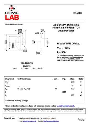
2N5933 Dimensions in mm (inches). Bipolar NPN Device in a Hermetically sealed TO3 25.15 (0.99) 6.35 (0.25) 26.67 (1.05) 9.15 (0.36) Metal Package. 10.67 (0.42) 11.18 (0.44) 1.52 (0.06) 3.43 (0.135) 1 2 Bipolar NPN Device. 3 VCEO = 100V (case) 3.84 (0.151) 4.09 (0.161) 7.92 (0.312) IC = 30A 12.70 (0.50) All Semelab hermetically sealed products can be processed in
2n5971.pdf
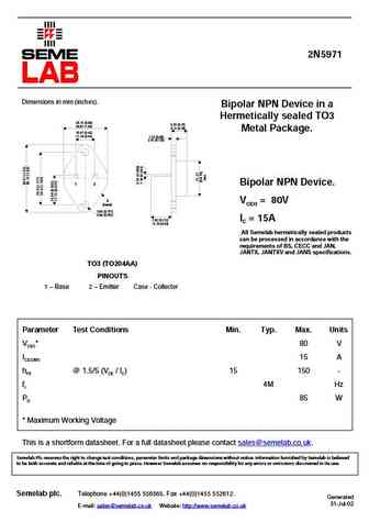
2N5971 Dimensions in mm (inches). Bipolar NPN Device in a Hermetically sealed TO3 25.15 (0.99) 6.35 (0.25) 26.67 (1.05) 9.15 (0.36) Metal Package. 10.67 (0.42) 11.18 (0.44) 1.52 (0.06) 3.43 (0.135) 1 2 Bipolar NPN Device. 3 VCEO = 80V (case) 3.84 (0.151) 4.09 (0.161) 7.92 (0.312) IC = 15A 12.70 (0.50) All Semelab hermetically sealed products can be processed in a
2n5936.pdf

2N5936 Dimensions in mm (inches). Bipolar NPN Device in a Hermetically sealed TO3 25.15 (0.99) 6.35 (0.25) 26.67 (1.05) 9.15 (0.36) Metal Package. 10.67 (0.42) 11.18 (0.44) 1.52 (0.06) 3.43 (0.135) 1 2 Bipolar NPN Device. 3 VCEO = 120V (case) 3.84 (0.151) 4.09 (0.161) 7.92 (0.312) IC = 30A 12.70 (0.50) All Semelab hermetically sealed products can be processed in
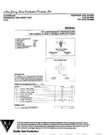
2n5945.pdf
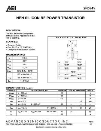
2N5945 NPN SILICON RF POWER TRANSISTOR DESCRIPTION The ASI 2N5945 is Designed for FM Land Mobile Applications in the PACKAGE STYLE .280 4L STUD 400 to 960 MHz. A 45 FEATURES C Common Emitter B E E PG = 9.0 dB at 2.0 W/470 MHz B Omnigold Metalization System C D J E I MAXIMUM RATINGS F G IC 0.8 A H #8-32 UNC K VCBO 36 V MINIMUM
2n5911 2n5912.pdf
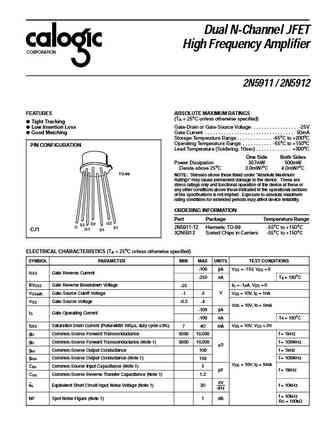
Dual N-Channel JFET High Frequency Amplifier CORPORATION 2N5911 / 2N5912 FEATURES ABSOLUTE MAXIMUM RATINGS (T = 25oC unless otherwise specified) A Tight Tracking Low Insertion Loss Gate-Drain or Gate-Source Voltage . . . . . . . . . . . . . . . . -25V Good Matching Gate Current . . . . . . . . . . . . . . . . . . . . . . . . . . . . . . . . . 50mA Storage Te
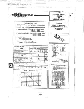
2n5989 2n5990 2n5991.pdf
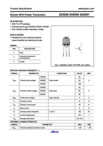
Product Specification www.jmnic.com Silicon NPN Power Transistors 2N5989 2N5990 2N5991 DESCRIPTION With TO-3PN package Complement to type 2N5986 2N5987 2N5988 Low collector-emitter saturation voltage APPLICATIONS Designed for use in general purpose power amplifier and switching circuits. PINNING PIN DESCRIPTION 1 Base Collector;connected to 2 mounting base 3
2n5972.pdf
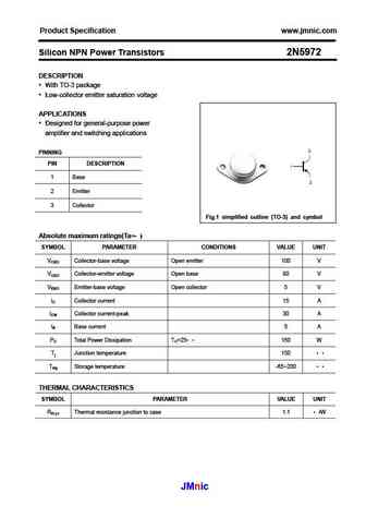
Product Specification www.jmnic.com Silicon NPN Power Transistors 2N5972 DESCRIPTION With TO-3 package Low-collector emitter saturation voltage APPLICATIONS Designed for general-purpose power amplifier and switching applications PINNING PIN DESCRIPTION 1 Base 2 Emitter 3 Collector Fig.1 simplified outline (TO-3) and symbol Absolute maximum ratings(Ta= ) SYMBOL
2n5973.pdf
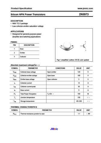
Product Specification www.jmnic.com Silicon NPN Power Transistors 2N5973 DESCRIPTION With TO-3 package Low collector-emitter saturation voltage APPLICATIONS Designed for general-purpose power amplifier and switching applications PINNING PIN DESCRIPTION 1 Base 2 Emitter 3 Collector Fig.1 simplified outline (TO-3) and symbol Absolute maximum ratings(Ta= ) SYMBOL
2n5970.pdf
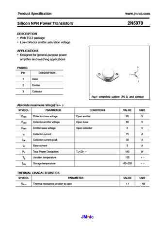
Product Specification www.jmnic.com Silicon NPN Power Transistors 2N5970 DESCRIPTION With TO-3 package Low-collector emitter saturation voltage APPLICATIONS Designed for general-purpose power amplifier and switching applications PINNING PIN DESCRIPTION 1 Base 2 Emitter 3 Collector Fig.1 simplified outline (TO-3) and symbol Absolute maximum ratings(Ta= ) SYMBOL
2n5954 2n5955 2n5956.pdf
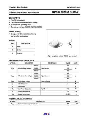
Product Specification www.jmnic.com Silicon PNP Power Transistors 2N5954 2N5955 2N5956 DESCRIPTION With TO-66 package Low collector-emitter saturation voltage Excellent safe operating area Complement to type 2N6372 2N6373 2N6374 APPLICATIONS Designed for driver circuits,switching and amplifier applications PINNING PIN DESCRIPTION 1 Base 2 Emitter 3 Collector
2n5419 2n5420 2n5550 2n5551 2n5830 2n5831 2n5832 2n5998 2n5999 2n6008 2n6009 2n6076 2n6426 2n6427.pdf
2n5935.pdf
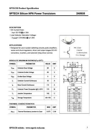
SPTECH Product Specification SPTECH Silicon NPN Power Transistors 2N5935 DESCRIPTION DC Current Gain- h = 20-100@I = 30A FE C Low Collector Saturation Voltage- V )= 2.0V(Max)@ I = 20A CE(sat C APPLICATIONS Designed for use in power switching circuits,audio amplifiers, series and shunt-regulators, driver and output stages,DC-DC converters, inverters, and solenoid /relay dri
2n5989.pdf

isc Silicon NPN Power Transistor 2N5989 DESCRIPTION Collector-Emitter Breakdown Voltage- V = 60V(Min) (BR)CEO Low Collector-Emitter Saturation Voltage 100% avalanche tested Minimum Lot-to-Lot variations for robust device performance and reliable operation APPLICATIONS Designed for use in general purpose amplifier and switching circuits ABSOLUTE MAXIMUM RATINGS(T =25 )
2n5989 2n5990 2n5991.pdf
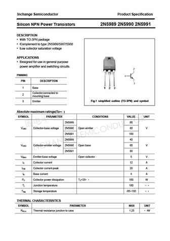
Inchange Semiconductor Product Specification Silicon NPN Power Transistors 2N5989 2N5990 2N5991 DESCRIPTION With TO-3PN package Complement to type 2N5986/5987/5988 Low collector saturation voltage APPLICATIONS Designed for use in general purpose power amplifier and switching circuits. PINNING PIN DESCRIPTION 1 Base Collector;connected to 2 mounting base Fig.
2n5972.pdf
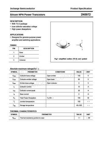
Inchange Semiconductor Product Specification Silicon NPN Power Transistors 2N5972 DESCRIPTION With TO-3 package Low collector saturation voltage High power dissipations APPLICATIONS Designed for general-purpose power amplifier and switching applications PINNING PIN DESCRIPTION 1 Base 2 Emitter Fig.1 simplified outline (TO-3) and symbol 3 Collector Absolute max
2n5991.pdf
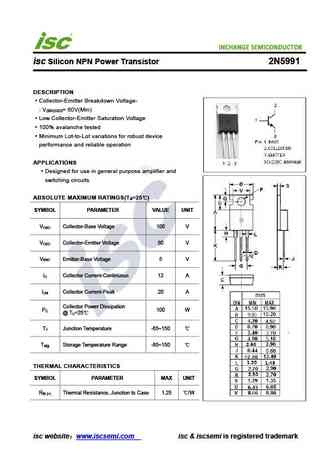
isc Silicon NPN Power Transistor 2N5991 DESCRIPTION Collector-Emitter Breakdown Voltage- V = 60V(Min) (BR)CEO Low Collector-Emitter Saturation Voltage 100% avalanche tested Minimum Lot-to-Lot variations for robust device performance and reliable operation APPLICATIONS Designed for use in general purpose amplifier and switching circuits ABSOLUTE MAXIMUM RATINGS(T =25 )
2n5973.pdf

Inchange Semiconductor Product Specification Silicon NPN Power Transistors 2N5973 DESCRIPTION With TO-3 package Low collector saturation voltage High power dissipations APPLICATIONS Designed for general-purpose power amplifier and switching applications PINNING PIN DESCRIPTION 1 Base 2 Emitter Fig.1 simplified outline (TO-3) and symbol 3 Collector Absolute max
2n5970.pdf
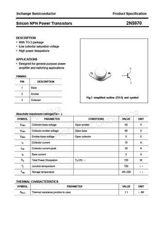
Inchange Semiconductor Product Specification Silicon NPN Power Transistors 2N5970 DESCRIPTION With TO-3 package Low collector saturation voltage High power dissipations APPLICATIONS Designed for general-purpose power amplifier and switching applications PINNING PIN DESCRIPTION 1 Base 2 Emitter Fig.1 simplified outline (TO-3) and symbol 3 Collector Absolute max
2n5954 2n5955 2n5956.pdf
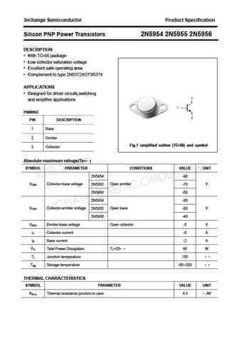
Inchange Semiconductor Product Specification Silicon PNP Power Transistors 2N5954 2N5955 2N5956 DESCRIPTION With TO-66 package Low collector saturation voltage Excellent safe operating area Complement to type 2N6372/6373/6374 APPLICATIONS Designed for driver circuits,switching and amplifier applications PINNING PIN DESCRIPTION 1 Base 2 Emitter Fig.1 simplifie
Другие транзисторы: 2N5892, 2N5893, 2N5894, 2N5895, 2N5896, 2N5897, 2N5898, 2N5899, TIP120, 2N5900, 2N5901, 2N591, 2N5910, 2N5913, 2N5914, 2N5915, 2N591-5
🌐 : EN ES РУ

Список транзисторов
Обновления
BJT: GA1A4M | SBT42 | 2SA200-Y | 2SA200-O | 2SD882-Q | 2SD882-P | 2SD882-E | 2SC945-L | 2SC945-H | 2SC4226-R23 | 2SC3357-F | 2SC3357-E | 2SC3356-R26 | 2SC3356-R24 | 2SC3356-R23 | 2SB772-Q | 2SB772-P | 2SB772-E | 2SA1015-L | 2SA1015-H | HSS8550
Popular searches
2sc732 | 2sc1451 replacement | 6426 mosfet | b1565 | nce82h140 | 2n2369 equivalent | 2sd313 datasheet | k8a50d datasheet