2N61. Аналоги и основные параметры
Наименование производителя: 2N61
Тип материала: Ge
Полярность: PNP
Предельные значения
Максимальная рассеиваемая мощность (Pc): 0.18 W
Макcимально допустимое напряжение коллектор-база (Ucb): 25 V
Макcимально допустимое напряжение эмиттер-база (Ueb): 10 V
Макcимальный постоянный ток коллектора (Ic): 0.2 A
Предельная температура PN-перехода (Tj): 85 °C
Электрические характеристики
Граничная частота коэффициента передачи тока (ft): 0.4 MHz
Ёмкость коллекторного перехода (Cc): 80 pf
Статический коэффициент передачи тока (hFE): 45
Корпус транзистора: TO5
Аналоги (замена) для 2N61
- подборⓘ биполярного транзистора по параметрам
2N61 даташит
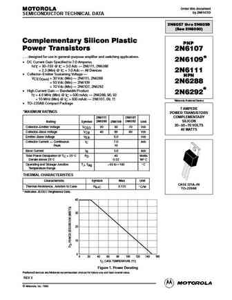
2n6107 2n6111 2n6288 2n6109 2n6292.pdf
Order this document MOTOROLA by 2N6107/D SEMICONDUCTOR TECHNICAL DATA 2N6057 thru 2N6059 (See 2N6050) Complementary Silicon Plastic PNP Power Transistors 2N6107 . . . designed for use in general purpose amplifier and switching applications. 2N6109* DC Current Gain Specified to 7.0 Amperes hFE = 30 150 @ IC = 3.0 Adc 2N6111, 2N6288 hFE = 2.3 (Min) @ IC = 7.0 Adc All
2n6107 2n6111.pdf
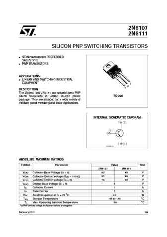
2N6107 2N6111 SILICON PNP SWITCHING TRANSISTORS STMicroelectronics PREFERRED SALESTYPE PNP TRANSISTORS APPLICATIONS LINEAR AND SWITCHING INDUSTRIAL EQUIPMENT 3 2 1 DESCRIPTION The 2N6107 and 2N6111 are epitaxial-base PNP TO-220 silicon transistors in Jedec TO-220 plastic package. They are intended for a wide variety of medium power switching and linear applications
2n6111.pdf
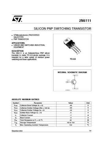
2N6111 SILICON PNP SWITCHING TRANSISTOR STMicroelectronics PREFERRED SALESTYPE PNP TRANSISTOR APPLICATIONS LINEAR AND SWITCHING INDUSTRIAL EQUIPMENT DESCRIPTION 3 2 The 2N6111 is an Epitaxial-Base PNP silicon 1 transistor in Jedec TO-220 plastic package. It is intended for a wide variety of medium power TO-220 switching and linear applications. INTERNAL SCHEMATIC DIA
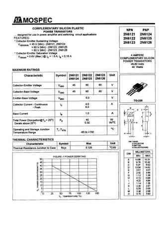
2n6121 2n6122 2n6123 2n6124 2n6125 2n6126.pdf
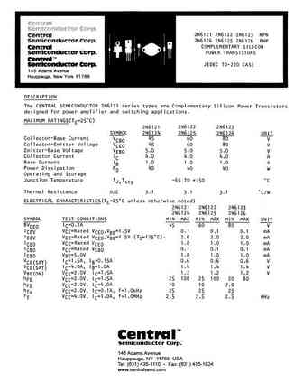
TM Central Semiconductor Corp. 145 Adams Avenue Hauppauge, NY 11788 USA Tel (631) 435-1110 Fax (631) 435-1824 www.centralsemi.com
2n6190 2n6191 2n6192 2n6193.pdf
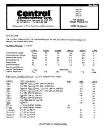
145 Adams Avenue, Hauppauge, NY 11788 USA Tel (631) 435-1110 Fax (631) 435-1824
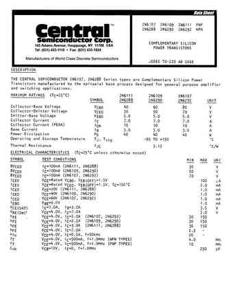
2n6107 2n6109 2n6111 2n6288 2n6290 2n6292.pdf
145 Adams Avenue, Hauppauge, NY 11788 USA Tel (631) 435-1110 Fax (631) 435-1824
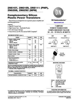
2n6107g 2n6109g 2n6111g 2n6288g 2n6292g.pdf
2N6107, 2N6109, 2N6111 (PNP), 2N6288, 2N6292 (NPN) Complementary Silicon Plastic Power Transistors These devices are designed for use in general-purpose amplifier and switching applications. www.onsemi.com Features 7 AMPERE High DC Current Gain High Current Gain - Bandwidth Product POWER TRANSISTORS TO-220 Compact Package COMPLEMENTARY SILICON These Devices are Pb-
2n6109g 2n6109g 2n6107g.pdf
2N6107, 2N6109, 2N6111 (PNP), 2N6288, 2N6292 (NPN) Complementary Silicon Plastic Power Transistors These devices are designed for use in general-purpose amplifier and switching applications. www.onsemi.com Features 7 AMPERE High DC Current Gain High Current Gain - Bandwidth Product POWER TRANSISTORS TO-220 Compact Package COMPLEMENTARY SILICON These Devices are Pb-
2n6107 2n6109 2n6111 2n6288 2n6292.pdf
2N6107, 2N6109, 2N6111 (PNP), 2N6288, 2N6292 (NPN) Complementary Silicon Plastic Power Transistors These devices are designed for use in general-purpose amplifier and switching applications. www.onsemi.com Features 7 AMPERE High DC Current Gain High Current Gain - Bandwidth Product POWER TRANSISTORS TO-220 Compact Package COMPLEMENTARY SILICON These Devices are Pb-
2n6107g.pdf
2N6107, 2N6109, 2N6111 (PNP), 2N6288, 2N6292 (NPN) Complementary Silicon Plastic Power Transistors These devices are designed for use in general-purpose amplifier and switching applications. www.onsemi.com Features 7 AMPERE High DC Current Gain High Current Gain - Bandwidth Product POWER TRANSISTORS TO-220 Compact Package COMPLEMENTARY SILICON These Devices are Pb-
2n6111g 2n6111g 2n6292g.pdf
2N6107, 2N6109, 2N6111 (PNP), 2N6288, 2N6292 (NPN) Complementary Silicon Plastic Power Transistors These devices are designed for use in general-purpose amplifier and switching applications. www.onsemi.com Features 7 AMPERE High DC Current Gain High Current Gain - Bandwidth Product POWER TRANSISTORS TO-220 Compact Package COMPLEMENTARY SILICON These Devices are Pb-
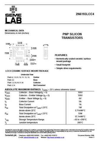
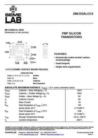
2n6193lcc4.pdf
2N6193LCC4 MECHANICAL DATA Dimensions in mm (inches) PNP SILICON TRANSISTORS 9.14 (0.360) 1.27 (0.050) 8.64 (0.340) 1.07 (0.040) 2.16 (0.085) 12 13 14 15 16 1.39 (0.055) 1.02 (0.040) 11 17 10 18 7.62 (0.300) 7.12 (0.280) 9 1 0.76 (0.030) FEATURES 8 2 0.51 (0.020) Hermetically sealed ceramic surface 0.33 (0.013) Rad. 0.08 (0.003) 7 6 5 4 3 mount package 0.43 (0
2n6193alcc4.pdf
2N6193ALCC4 MECHANICAL DATA Dimensions in mm (inches) PNP SILICON TRANSISTORS 9.14 (0.360) 1.27 (0.050) 8.64 (0.340) 1.07 (0.040) 2.16 (0.085) 12 13 14 15 16 1.39 (0.055) 1.02 (0.040) 11 17 10 18 7.62 (0.300) 7.12 (0.280) 9 1 0.76 (0.030) FEATURES 8 2 0.51 (0.020) Hermetically sealed ceramic surface 0.33 (0.013) Rad. 0.08 (0.003) 7 6 5 4 3 mount package 0.43 (
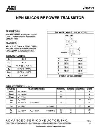
2n6199.pdf
2N6199 NPN SILICON RF POWER TRANSISTOR DESCRIPTION PACKAGE STYLE .380" 4L STUD The ASI 2N6199 is Designed for VHF .112x45 A Class C Power Amplifier Applications C up to 250 MHz. B E E FEATURES C B PG = 10 dB Typical at 25 W/175 MHz I Load VSWR at Rated Conditions D H J Omnigold Metallization System G #8-32 UNC-2A F E MA
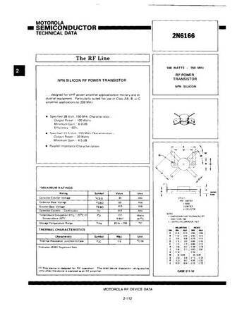
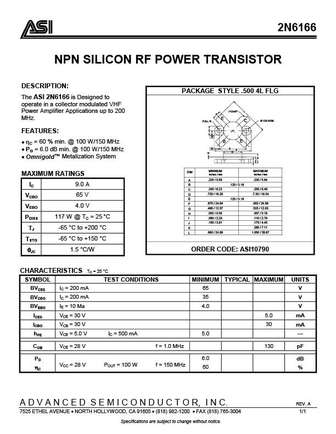
2n6166.pdf
2N6166 NPN SILICON RF POWER TRANSISTOR DESCRIPTION PACKAGE STYLE .500 4L FLG The ASI 2N6166 is Designed to operate in a collector modulated VHF .112x45 L Power Amplifier Applications up to 200 A MHz. E .125 NOM. C FULL R C FEATURES B E B C = 60 % min. @ 100 W/150 MHz E D PG = 6.0 dB min. @ 100 W/150 MHz F G H Omnigold Metalization Sy
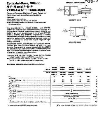
2n6106 2n6107 2n6108 2n6109 2n6110 2n6111 2n6288 2n6289 2n6290 2n6291 2n6292 2n6293 2n6473 2n6474 2n6475 2n6476.pdf
Boca Semiconductor Corp. BSC http //www.bocasemi.com http //www.bocasemi.com
2n6107 2n6292.pdf
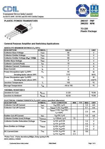
Continental Device India Limited An ISO/TS 16949, ISO 9001 and ISO 14001 Certified Company PLASTIC POWER TRANSISTORS 2N6107 PNP 2N6292 NPN TO-220 Plastic Package General Purpose Amplifier and Switching Applications ABSOLUTE MAXIMUM RATINGS (Ta=25 C) DESCRIPTION SYMBOL VALUE UNIT VCBO Collector Base Voltage 80 V Collector Emitter Voltage VCEO 70 V Collector Emitter Voltage (RBE= 100
2n6121-26.pdf
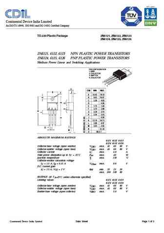
Continental Device India Limited An ISO/TS 16949, ISO 9001 and ISO 14001 Certified Company TO-220 Plastic Package 2N6121, 2N6122, 2N6123 2N6124, 2N6125, 2N6126 2N6121, 6122, 6123 NPN PLASTIC POWER TRANSISTORS 2N6124, 6125, 6126 PNP PLASTIC POWER TRANSISTORS Medium Power Linear and Switching Applications PIN CONFIGURATION 4 1. BASE 2. COLLECTOR 3. EMITTER 4. COLLECTOR 1 2 3 C DI
2n6101.pdf
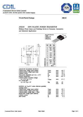
Continental Device India Limited An ISO/TS 16949, ISO 9001 and ISO 14001 Certified Company TO-220 Plastic Package 2N6101 2N6101 NPN PLASTIC POWER TRANSISTOR Medium Power Linear and Switching Service in Consumer, Automotive, and Industrial Applications PIN CONFIGURATION 4 1. BASE 2. COLLECTOR 3. EMITTER 4. COLLECTOR 1 2 3 C DIM MIN. MAX. B E F A 14.42 16.51 B 9.63 10.67 C 3.
2n6111.pdf
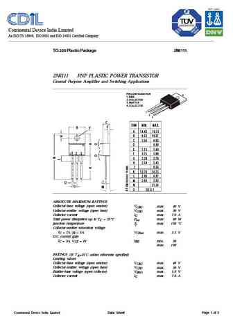
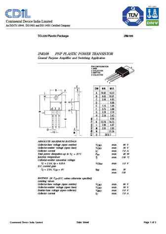
Continental Device India Limited An ISO/TS 16949, ISO 9001 and ISO 14001 Certified Company TO-220 Plastic Package 2N6111 2N6111 PNP PLASTIC POWER TRANSISTOR General Purpose Amplifier and Switching Applications PIN CONFIGURATION 4 1. BASE 2. COLLECTOR 3. EMITTER 4. COLLECTOR 1 2 3 C DIM MIN. MAX. E B F A 14.42 16.51 B 9.63 10.67 C 3.56 4.83 D0.90 E 1.15 1.40 1 2 3 F 3.75
2n6109.pdf
Continental Device India Limited An ISO/TS 16949, ISO 9001 and ISO 14001 Certified Company TO-220 Plastic Package 2N6109 2N6109 PNP PLASTIC POWER TRANSISTOR General Purpose Amplifier and Switching Application PIN CONFIGURATION 4 1. BASE 2. COLLECTOR 3. EMITTER 4. COLLECTOR 1 2 3 C DIM MIN. MAX. E B F A 14.42 16.51 B 9.63 10.67 C 3.56 4.83 D0.90 E 1.15 1.40 1 2 3 F 3.75
2n6102 2n6103.pdf
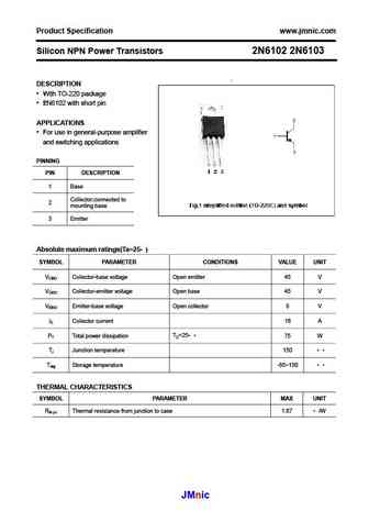
Product Specification www.jmnic.com Silicon NPN Power Transistors 2N6102 2N6103 DESCRIPTION With TO-220 package 2N6102 with short pin APPLICATIONS For use in general-purpose amplifier and switching applications PINNING PIN DESCRIPTION 1 Base Collector;connected to 2 mounting base 3 Emitter Absolute maximum ratings(Ta=25 ) SYMBOL PARAMETER CONDITIONS VALUE
2n6098 2n6099 2n6100 2n6101.pdf
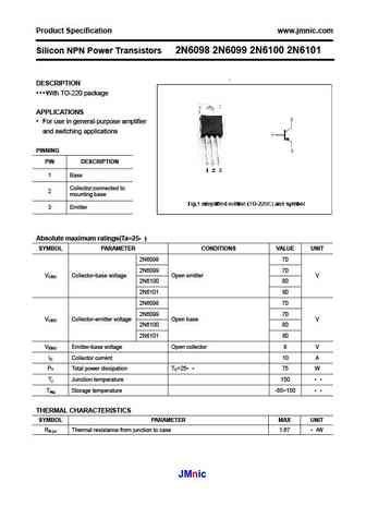
Product Specification www.jmnic.com Silicon NPN Power Transistors 2N6098 2N6099 2N6100 2N6101 DESCRIPTION With TO-220 package APPLICATIONS For use in general-purpose amplifier and switching applications PINNING PIN DESCRIPTION 1 Base Collector;connected to 2 mounting base 3 Emitter Absolute maximum ratings(Ta=25 ) SYMBOL PARAMETER CONDITIONS VALUE UNIT 2N
2n6129 2n6130 2n6131.pdf
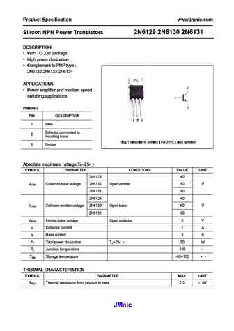
Product Specification www.jmnic.com Silicon NPN Power Transistors 2N6129 2N6130 2N6131 DESCRIPTION With TO-220 package High power dissipation Complement to PNP type 2N6132 2N6133 2N6134 APPLICATIONS Power amplifier and medium speed switching applications PINNING PIN DESCRIPTION 1 Base Collector;connected to 2 mounting base 3 Emitter Absolute maximum r
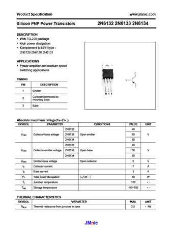
2n6132 2n6133 2n6134.pdf
Product Specification www.jmnic.com Silicon PNP Power Transistors 2N6132 2N6133 2N6134 DESCRIPTION With TO-220 package High power dissipation Complement to NPN type 2N6129 2N6130 2N6131 APPLICATIONS Power amplifier and medium speed switching applications PINNING PIN DESCRIPTION 1 Emitter Collector;connected to 2 mounting base 3 Base Absolute maximum ra
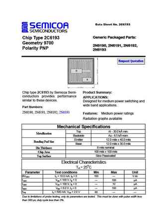
2n6193.pdf
Data Sheet No. 2C6193 Generic Packaged Parts Chip Type 2C6193 Geometry 9700 2N6190, 2N6191, 2N6192, Polarity PNP 2N6193 Chip type 2C6193 by Semicoa Semi- Product Summary conductors provides performance APPLICATIONS similar to these devices. Designed for medium power switching and wide band applications. Part Numbers 2N6190, 2N6191, 2N6192, 2N6193 Features Medium power rating
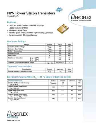
2n6193u3.pdf
NPN Power Silicon Transistors 2N6193U3 Features JANS and JANSR Qualified to MIL-PRF-19500/561 JEDEC resistered 2N6193 Lightweight & Low Power Ideal for Space, Military and Other High Reliability Applications Surface mount U3 (TO-276AA) Package Maximum Ratings Ratings Symbol Value Units Collector - Emitter Voltage VCEO 100 Vdc Collector - Base Voltage VCBO 100 Vdc
2n6193.pdf
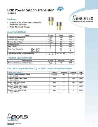
PNP Power Silicon Transistor 2N6193 Features Available in JAN, JANTX, JANTXV and JANS per MIL-PRF-19500/561 TO-39 (TO-205AD) Package Maximum Ratings Ratings Symbol Value Units Collector - Emitter Voltage VCEO 100 Vdc Collector - Base Voltage VCBO 100 Vdc Emitter - Base Voltage VEBO 6.0 Vdc Collector Current IC 5.0 Adc Base Current IB 1.0 Adc Total Power Dissipation @ TA =
2n6124.pdf
INCHANGE Semiconductor isc Silicon PNP Power Transistor 2N6124 DESCRIPTION Collector-Emitter Sustaining Voltage- V = -0.6V(Max.)@ I = -1.5A CE(sat) C Collector-Emitter Sustaining Voltage- V = -45V(Min) CEO(SUS) Complement to Type 2N6121 Minimum Lot-to-Lot variations for robust device performance and reliable operation APPLICATIONS Designed for use in power amplifier a
2n6122.pdf
INCHANGE Semiconductor isc Silicon NPN Power Transistor 2N6122 DESCRIPTION Collector-Emitter Sustaining Voltage- V = 0.6V(Max.)@ I = 1.5A CE(sat) C Collector-Emitter Sustaining Voltage- V = 60V(Min) CEO(SUS) Complement to Type 2N6125 Minimum Lot-to-Lot variations for robust device performance and reliable operation APPLICATIONS Designed for use in power amplifier and
2n6107.pdf
INCHANGE Semiconductor isc Silicon PNP Power Transistor 2N6107 DESCRIPTION DC Current Gain- h = 30-150@ I = -2A FE C Collector-Emitter Sustaining Voltage- V = -70V(Min) CEO(SUS) Complement to Type 2N6292 Minimum Lot-to-Lot variations for robust device performance and reliable operation APPLICATIONS Designed for use in general-purpose amplifier and switching applicati
2n6121.pdf
INCHANGE Semiconductor isc Silicon NPN Power Transistor 2N6121 DESCRIPTION Collector-Emitter Sustaining Voltage- V = 0.6V(Max.)@ I = 1.5A CE(sat) C Collector-Emitter Sustaining Voltage- V = 45V(Min) CEO(SUS) Complement to Type 2N6124 Minimum Lot-to-Lot variations for robust device performance and reliable operation APPLICATIONS Designed for use in power amplifier and
2n6126.pdf
INCHANGE Semiconductor isc Silicon PNP Power Transistor 2N6126 DESCRIPTION Collector-Emitter Sustaining Voltage- V = -0.6V(Max.)@ I = -1.5A CE(sat) C Collector-Emitter Sustaining Voltage- V = -80V(Min) CEO(SUS) Complement to Type 2N6123 Minimum Lot-to-Lot variations for robust device performance and reliable operation APPLICATIONS Designed for use in power amplifier a
2n6130.pdf
INCHANGE Semiconductor isc Silicon NPN Power Transistor 2N6130 DESCRIPTION DC Current Gain- h = 20-100@ I = 2.5A FE C Collector-Emitter Sustaining Voltage- V = 60V(Min) CEO(SUS) Complement to Type 2N6133 Minimum Lot-to-Lot variations for robust device performance and reliable operation APPLICATIONS Designed for use in power amplifier and switching circuits applicatio
2n6103.pdf
isc Silicon NPN Power Transistor 2N6103 DESCRIPTION DC Current Gain - h = 15-60@ I = 8A FE C Collector-Emitter Sustaining Voltage- V = 40V(Min) CEO(SUS) Minimum Lot-to-Lot variations for robust device performance and reliable operation APPLICATIONS Designed for use in medium power liner amplifier and switching service in consumer ,automotive and industrial applications.
2n6110.pdf
INCHANGE Semiconductor isc Silicon PNP Power Transistor 2N6110 DESCRIPTION DC Current Gain- h = 30-150@ I = -3A FE C Collector-Emitter Sustaining Voltage- V = -30V(Min) CEO(SUS) Minimum Lot-to-Lot variations for robust device performance and reliable operation APPLICATIONS Power amplifier and switching circuits applications ABSOLUTE MAXIMUM RATINGS(T =25 ) a SY
2n6124 2n6125 2n6126.pdf
Inchange Semiconductor Product Specification Silicon PNP Power Transistors 2N6124 2N6125 2N6126 DESCRIPTION With TO-220 package Complement to PNP type 2N6121 ;2N6122 ;2N6123 APPLICATIONS For use in power amplifier and switching circuit applications PINNING PIN DESCRIPTION 1 Emitter Collector;connected to 2 mounting base Fig.1 simplified outline (TO-220) and
2n6102 2n6103.pdf
Inchange Semiconductor Product Specification Silicon NPN Power Transistors 2N6102 2N6103 DESCRIPTION With TO-220 package 2N6102 type with short pin APPLICATIONS For use in general-purpose amplifier and switching applications PINNING PIN DESCRIPTION 1 Base Collector;connected to 2 mounting base 3 Emitter Absolute maximum ratings(Ta=25 ) SYMBOL PARAMETER CON
2n6098 2n6099 2n6100 2n6101.pdf
Inchange Semiconductor Product Specification Silicon NPN Power Transistors 2N6098 2N6099 2N6100 2N6101 DESCRIPTION With TO-220 package High current capability APPLICATIONS For use in general-purpose amplifier and switching applications PINNING PIN DESCRIPTION 1 Base Collector;connected to 2 mounting base 3 Emitter Absolute maximum ratings(Ta=25 ) SYMBOL PA
2n6121 2n6122 2n6123.pdf
Inchange Semiconductor Product Specification Silicon NPN Power Transistors 2N6121 2N6122 2N6123 DESCRIPTION With TO-220 package Complement to PNP type 2N6124 ;2N6125 ;2N6126 APPLICATIONS For use in power amplifier and switching circuit applications PINNING PIN DESCRIPTION 1 Base Collector;connected to 2 mounting base 3 Emitter Absolute maximum ratings(Ta=
2n6106.pdf
INCHANGE Semiconductor isc Silicon PNP Power Transistor 2N6106 DESCRIPTION DC Current Gain- h = 30-150@ I = -2A FE C Collector-Emitter Sustaining Voltage- V = -70V(Min) CEO(SUS) Minimum Lot-to-Lot variations for robust device performance and reliable operation APPLICATIONS Designed for use in general-purpose amplifier and switching applications ABSOLUTE MAXIMUM RATINGS
2n6106 2n6108 2n6110.pdf
Inchange Semiconductor Product Specification Silicon PNP Power Transistors 2N6106 2N6108 2N6110 DESCRIPTION With TO-220 package With short pin APPLICATIONS Power amplifier and switching circuits applications PINNING PIN DESCRIPTION 1 Emitter Collector;connected to 2 mounting base Fig.1 simplified outline (TO-220) and symbol 3 Base Absolute maximum ratings(Ta=2
2n6131.pdf
INCHANGE Semiconductor isc Silicon NPN Power Transistor 2N6131 DESCRIPTION DC Current Gain- h = 20-100@ I = 2.5A FE C Collector-Emitter Sustaining Voltage- V = 80V(Min) CEO(SUS) Complement to Type 2N6134 Minimum Lot-to-Lot variations for robust device performance and reliable operation APPLICATIONS Designed for use in power amplifier and switching circuits applicatio
2n6101.pdf
isc Silicon NPN Power Transistor 2N6101 DESCRIPTION DC Current Gain - h = 20-80@ I = 5A FE C Collector-Emitter Sustaining Voltage- V = 70V(Min) CEO(SUS) Minimum Lot-to-Lot variations for robust device performance and reliable operation APPLICATIONS Designed for use in medium power liner amplifier and switching service in consumer ,automotive and industrial applications.
2n6111.pdf
INCHANGE Semiconductor isc Silicon PNP Power Transistor 2N6111 DESCRIPTION DC Current Gain- h = 30-150@ I = -3A FE C Collector-Emitter Sustaining Voltage- V = -30V(Min) CEO(SUS) Minimum Lot-to-Lot variations for robust device performance and reliable operation APPLICATIONS Designed for use in general-purpose amplifier and switching applications ABSOLUTE MAXIMUM RATINGS
2n6129 2n6130 2n6131.pdf
Inchange Semiconductor Product Specification Silicon NPN Power Transistors 2N6129 2N6130 2N6131 DESCRIPTION With TO-220 package High power dissipation Complement to PNP type 2N6132 2N6133 2N6134 APPLICATIONS Power amplifier and medium speed switching applications PINNING PIN DESCRIPTION 1 Base Collector;connected to 2 mounting base 3 Emitter Absolute
2n6129.pdf
INCHANGE Semiconductor isc Silicon NPN Power Transistor 2N6129 DESCRIPTION DC Current Gain- h = 20-100@ I = 2.5A FE C Collector-Emitter Sustaining Voltage- V = 40V(Min) CEO(SUS) Complement to Type 2N6132 Minimum Lot-to-Lot variations for robust device performance and reliable operation APPLICATIONS Designed for use in power amplifier and switching circuits applicatio
2n6123.pdf
INCHANGE Semiconductor isc Silicon NPN Power Transistor 2N6123 DESCRIPTION Collector-Emitter Sustaining Voltage- V = 0.6V(Max.)@ I = 1.5A CE(sat) C Collector-Emitter Sustaining Voltage- V = 80V(Min) CEO(SUS) Complement to Type 2N6126 Minimum Lot-to-Lot variations for robust device performance and reliable operation APPLICATIONS Designed for use in power amplifier and
2n6108.pdf
isc Silicon PNP Power Transistor 2N6108 DESCRIPTION DC Current Gain- h = 30-150@ I = -2A FE C Collector-Emitter Sustaining Voltage- V = -50V(Min) CEO(SUS) Minimum Lot-to-Lot variations for robust device performance and reliable operation APPLICATIONS Designed for use in general-purpose amplifier and switching applications ABSOLUTE MAXIMUM RATINGS(T =25 ) a SYMBOL PA
2n6132.pdf
INCHANGE Semiconductor isc Silicon PNP Power Transistor 2N6132 DESCRIPTION DC Current Gain- h = 20-100@ I = -2.5A FE C Collector-Emitter Sustaining Voltage- V = -40V(Min) CEO(SUS) Complement to Type 2N6129 Minimum Lot-to-Lot variations for robust device performance and reliable operation APPLICATIONS Designed for use in general-purpose amplifier and switching applica
2n6109.pdf
INCHANGE Semiconductor isc Silicon PNP Power Transistor 2N6109 DESCRIPTION DC Current Gain- h = 30-150@ I = -2.5A FE C Collector-Emitter Sustaining Voltage- V = -50V(Min) CEO(SUS) Minimum Lot-to-Lot variations for robust device performance and reliable operation APPLICATIONS Designed for use in general-purpose amplifier and switching applications ABSOLUTE MAXIMUM RATIN
2n6107 2n6109 2n6111.pdf
Inchange Semiconductor Product Specification Silicon PNP Power Transistors 2N6107 2N6109 2N6111 DESCRIPTION With TO-220 package Complement to NPN type 2N6288; 2N6290 ;2N6292 APPLICATIONS Power amplifier and switching circuits applications PINNING PIN DESCRIPTION 1 Emitter Collector;connected to 2 mounting base Fig.1 simplified outline (TO-220) and symbol 3 B
2n6102.pdf
isc Silicon NPN Power Transistor 2N6102 DESCRIPTION DC Current Gain - h = 20-80@ I = 5A FE C Collector-Emitter Sustaining Voltage- V = 40V(Min) CEO(SUS) Minimum Lot-to-Lot variations for robust device performance and reliable operation APPLICATIONS Designed for use in general-purpose amplifier and switching applications. ABSOLUTE MAXIMUM RATINGS(T =25 ) a SYMBOL PAR
2n6132 2n6133 2n6134.pdf
Inchange Semiconductor Product Specification Silicon PNP Power Transistors 2N6132 2N6133 2N6134 DESCRIPTION With TO-220 package High power dissipation Complement to NPN type 2N6129 2N6130 2N6131 APPLICATIONS Power amplifier and medium speed switching applications PINNING PIN DESCRIPTION 1 Emitter Collector;connected to 2 mounting base Fig.1 simplified o
2n6100.pdf
isc Silicon NPN Power Transistor 2N6100 DESCRIPTION DC Current Gain - h = 20-80@ I = 5A FE C Collector-Emitter Sustaining Voltage- V = 70V(Min) CEO(SUS) 100% avalanche tested Minimum Lot-to-Lot variations for robust device performance and reliable operation APPLICATIONS Designed for use in general-purpose amplifier and switching applications. ABSOLUTE MAXIMUM RATINGS
2n6125.pdf
INCHANGE Semiconductor isc Silicon PNP Power Transistor 2N6125 DESCRIPTION Collector-Emitter Sustaining Voltage- V = -0.6V(Max.)@ I = -1.5A CE(sat) C Collector-Emitter Sustaining Voltage- V = -60V(Min) CEO(SUS) Complement to Type 2N6122 Minimum Lot-to-Lot variations for robust device performance and reliable operation APPLICATIONS Designed for use in power amplifier a
2n6133.pdf
INCHANGE Semiconductor isc Silicon PNP Power Transistor 2N6133 DESCRIPTION DC Current Gain- h = 20-100@ I = -2.5A FE C Collector-Emitter Sustaining Voltage- V = -60V(Min) CEO(SUS) Complement to Type 2N6130 Minimum Lot-to-Lot variations for robust device performance and reliable operation APPLICATIONS Designed for use in general-purpose amplifier and switching applica
2n6134.pdf
INCHANGE Semiconductor isc Silicon PNP Power Transistor 2N6134 DESCRIPTION DC Current Gain- h = 20-100@ I = -2.5A FE C Collector-Emitter Sustaining Voltage- V = -80V(Min) CEO(SUS) Complement to Type 2N6131 Minimum Lot-to-Lot variations for robust device performance and reliable operation APPLICATIONS Designed for use in general-purpose amplifier and switching applica
Другие транзисторы: 2N6095, 2N6096, 2N6097, 2N6098, 2N6099, 2N60A, 2N60B, 2N60C, BDT88, 2N610, 2N6100, 2N6101, 2N6102, 2N6103, 2N6104, 2N6105, 2N6106
History: WTD1386
🌐 : EN ES РУ
Список транзисторов
Обновления
BJT: GA1A4M | SBT42 | 2SA200-Y | 2SA200-O | 2SD882-Q | 2SD882-P | 2SD882-E | 2SC945-L | 2SC945-H | 2SC4226-R23 | 2SC3357-F | 2SC3357-E | 2SC3356-R26 | 2SC3356-R24 | 2SC3356-R23 | 2SB772-Q | 2SB772-P | 2SB772-E | 2SA1015-L | 2SA1015-H | HSS8550
Popular searches
2sc1327 | 2sc3855 | 2sc945 transistor equivalent | 2sd427 | mje15032 equivalent | 2sc4834 | 2sd313 transistor equivalent | 2sc871 replacement
