2SC3169 Datasheet. Specs and Replacement
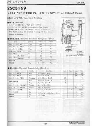
Type Designator: 2SC3169 📄📄
Material of Transistor: Si
Polarity: NPN
Absolute Maximum Ratings
Maximum Collector Power Dissipation (Pc): 25 W
Maximum Collector-Base Voltage |Vcb|: 500 V
Maximum Collector Current |Ic max|: 2 A
Max. Operating Junction Temperature (Tj): 150 °C
Electrical Characteristics
Transition Frequency (ft): 8 MHz
Forward Current Transfer Ratio (hFE), MIN: 55
Package: TO220
📄📄 Copy
2SC3169 Substitution
- BJT ⓘ Cross-Reference Search
2SC3169 datasheet
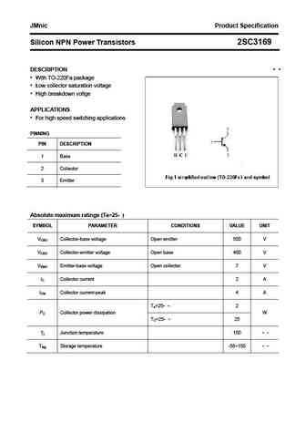
JMnic Product Specification Silicon NPN Power Transistors 2SC3169 DESCRIPTION With TO-220Fa package Low collector saturation voltage High breakdown voltge APPLICATIONS For high speed switching applications PINNING PIN DESCRIPTION 1 Base 2 Collector 3 Emitter Absolute maximum ratings (Ta=25 ) SYMBOL PARAMETER CONDITIONS VALUE UNIT VCBO Collector-base voltage... See More ⇒
isc Silicon NPN Power Transistor 2SC3169 DESCRIPTION Collector-Emiiter Sustaining Voltage- V = 400V(Min.) CEO(SUS) Low Collector Saturation Voltage V = 1.0V(Max.)@ I = 1A CE(sat) C High Speed Switching Minimum Lot-to-Lot variations for robust device performance and reliable operation APPLICATIONS Designed for high speed switching applications. ABSOLUTE MAXIMUM RATI... See More ⇒
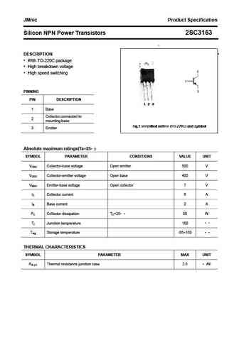
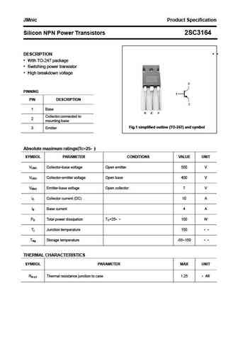
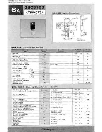
JMnic Product Specification Silicon NPN Power Transistors 2SC3163 DESCRIPTION With TO-220C package High breakdown voltage High speed switching PINNING PIN DESCRIPTION 1 Base Collector;connected to 2 mounting base 3 Emitter Absolute maximum ratings(Ta=25 ) SYMBOL PARAMETER CONDITIONS VALUE UNIT VCBO Collector-base voltage Open emitter 500 V VCEO Collector-e... See More ⇒
Detailed specifications: 2SC3161, 2SC3162, 2SC3163, 2SC3164, 2SC3165, 2SC3166, 2SC3167, 2SC3168, 2SD1047, 2SC317, 2SC3170, 2SC3171, 2SC3172, 2SC3173, 2SC3174, 2SC3175, 2SC3176
Keywords - 2SC3169 pdf specs
2SC3169 cross reference
2SC3169 equivalent finder
2SC3169 pdf lookup
2SC3169 substitution
2SC3169 replacement
BJT Parameters and How They Relate
History: 3DD13005F7
🌐 : EN ES РУ
LIST
Last Update
BJT: ZDT6705 | GA1L4Z | GA1A4M | SBT42 | 2SA200-Y | 2SA200-O
Popular searches
irlr8726 datasheet | ru7088r mosfet | mp40 transistor | fgpf4636 datasheet | 2sc1945 | c2383 | 2sb681 | bc639 equivalent
