5609 Specs and Replacement
Type Designator: 5609
Material of Transistor: Si
Polarity: NPN
Absolute Maximum Ratings
Maximum Collector Power Dissipation (Pc): 0.36 W
Maximum Collector-Base Voltage |Vcb|: 50 V
Maximum Collector-Emitter Voltage |Vce|: 45 V
Maximum Emitter-Base Voltage |Veb|: 5 V
Maximum Collector Current |Ic max|: 0.8 A
Max. Operating Junction Temperature (Tj): 150 °C
Electrical Characteristics
Transition Frequency (ft): 60 MHz
Collector Capacitance (Cc): 20 pF
Forward Current Transfer Ratio (hFE), MIN: 180
Noise Figure, dB: -
Package: TO92
5609 Substitution
5609 datasheet
tpt5609.pdf
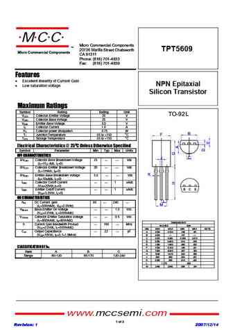
MCC Micro Commercial Components TM 20736 Marilla Street Chatsworth TPT5609 Micro Commercial Components CA 91311 Phone (818) 701-4933 Fax (818) 701-4939 Features Excellent linearity of Current Gain NPN Epitaxial Low saturation voltage Silicon Transistor Maximum Ratings Symbol Rating Rating Unit TO-92L VCEO Collector-Emitter Voltage 20 V VCBO Collector-Base Voltage 25 V ... See More ⇒
2sc5609.pdf
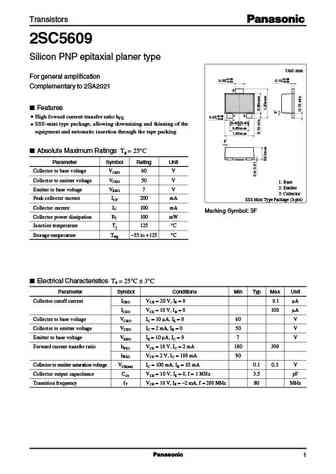
Transistors 2SC5609 Silicon PNP epitaxial planer type Unit mm For general amplification 0.33+0.05 0.10+0.05 0.02 0.02 Complementary to 2SA2021 3 Features High foward current transfer ratio hFE 0.23+0.05 1 2 0.02 (0.40) (0.40) SSS-mini type package, allowing downsizing and thinning of the 0.80 0.05 equipment and automatic insertion through the tape packing 1.2... See More ⇒
2n5609.pdf
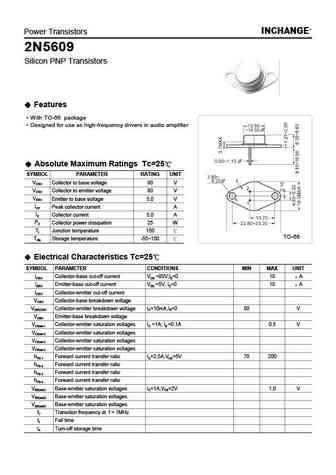
Power Transistors INCHANGE 2N5609 Silicon PNP Transistors Features With TO-66 package Designed for use as high-frequency drivers in audio amplifier Absolute Maximum Ratings Tc=25 SYMBOL PARAMETER RATING UNIT VCBO Collector to base voltage 80 V VCEO Collector to emitter voltage 80 V VEBO Emitter to base voltage 5.0 V ICP Peak collector current A IC Collector current 5.0 A PC... See More ⇒
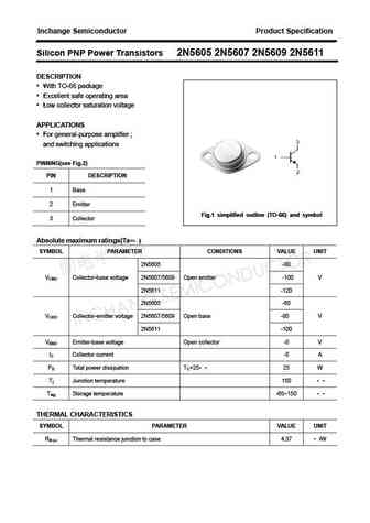
2n5605 2n5607 2n5609 2n5611.pdf
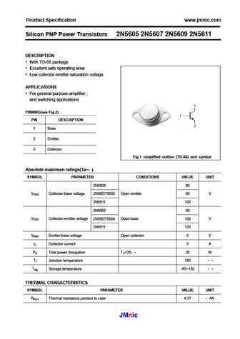
Product Specification www.jmnic.com Silicon PNP Power Transistors 2N5605 2N5607 2N5609 2N5611 DESCRIPTION With TO-66 package Excellent safe operating area Low collector-emitter saturation voltage APPLICATIONS For general-purpose amplifier ; and switching applications PINNING(see Fig.2) PIN DESCRIPTION 1 Base 2 Emitter 3 Collector Fig.1 simplified outline (TO-66)... See More ⇒
Detailed specifications: 50DA045D , 50DB040D , 50DB045D , 5253OA , 556BCYA , 556BCYB , 557BCYA , 557BCYB , MPSA42 , 5610 , 563BSY , 564BSY , 5NU72 , 5NU73 , 5NU74 , 60024 , 60DA060D .
Keywords - 5609 pdf specs
5609 cross reference
5609 equivalent finder
5609 pdf lookup
5609 substitution
5609 replacement


LIST
Last Update
BJT: GA1A4M | SBT42 | 2SA200-Y
Popular searches
3dd15d transistor | pa110bda | 2sb1243 | a1123 transistor | skd502t datasheet | svf7n65f | 2sc1419 datasheet | 2n4249 datasheet